 | –≠–ª–µ–∫—Ç—Ä–æ–Ω–Ω—ã–π –∫–æ–º–ø–æ–Ω–µ–Ω—Ç: TA2153FN | –°–∫–∞—á–∞—Ç—å:  PDF PDF  ZIP ZIP |
TA2153FN
2003-01-18
1
TOSHIBA Bipolar Linear Integrated Circuit Silicon Monolithic
TA2153FN
RF Amplifier for Digital Servo CD System
TA2153FN is a 3-beam type PUH compatible RF amplifier for
digital servo to be used in the CD system.
In combination with a CMOS single chip processor
TC9462F/TC9495F, a CD system can be composed very simply.
Features
∑ Built-in amplifier for reference (VRO, 2VRO) supply.
∑ Built-in auto laser power control circuit.
∑ Built-in RF amplifier.
∑ Built-in AGC amplifier.
∑ Built-in focus error amp and tracking error amp.
∑ Built-in sub-beam adder signal amplifier.
∑ Built-in gain change circuit for CD-RW.
∑ Capable of tracking balance control with TC9462F/TC9495F.
∑ Capable of RF gain adjustment circuit with TC9462F/TC9495F.
∑ Built-in signal amplifier for track counter.
∑ Capable of 4 times speed operation.
∑ 30 pin mini flat package.
Weight: 0.17 g (typ.)
TA2153FN
2003-01-18
2
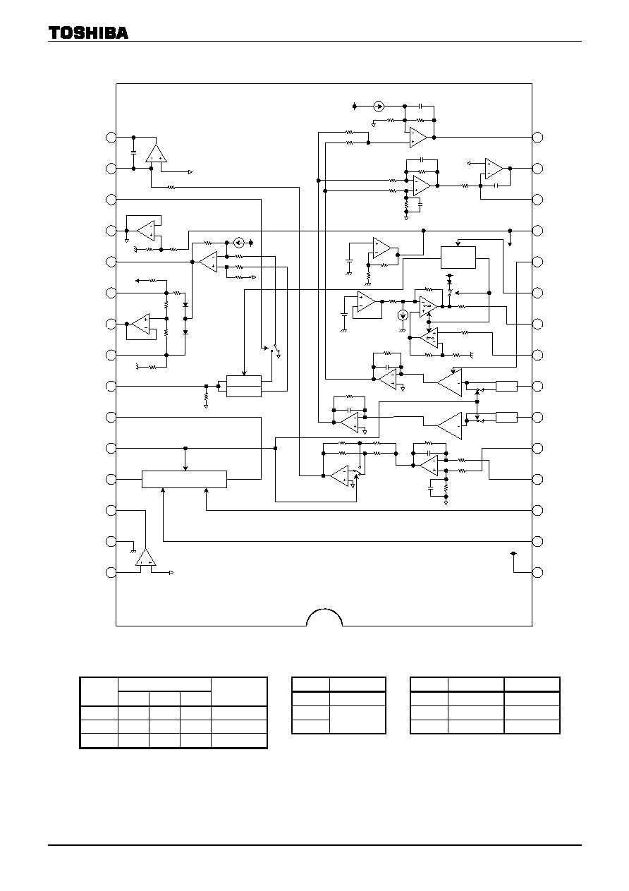
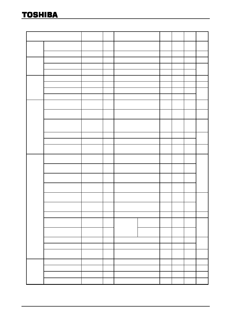
Block Diagram
LDC GVSW
Mode
SEB
Bottom
Detect
Peak
Detect
SEL
SW1 SW2 SW3
RFRP Detect
Frequency
GND CD-RW
GND ON
ON
GND
ON
OFF
OFF Low
HiZ
HiZ
ON
ON
HiZ OFF ON ON
Low
V
CC
Normal
V
CC
OFF
ON
V
CC
OFF
ON
ON High
15
14
13
12
11
10
9
8
7
6
5
4
3
2
1
RFN2
GND
RFO
AGCIN
GVSW
RFGO
RFRPIN
PKC
RFCT
BTC
RFRP
VRO
SEB
FEN
FEO
SBAD
TEO
TEN
TEB
SEL
2VRO
LDO
MDI
TNI
TPI
FPI
FNI
GMAD
RFGC
V
CC
15 pF
15 pF
238 k
9
238 k
9
13 k
9
2.26 k
9
1.4 k
9
1 k
9
83 k
9
2.9 k
9
48 k
9
21.
82 k
9
3 STATE
DET.
20 k
9
3 pF
10 k
9
10 k
9
50 k
9
36 pF
15 k
9
15 k
9
10 pF
30 k
9
1 k
9
40 pF
150 k
9
60 k
9
10 pF
20 k
9
20 k
9
20 k
9
12 k
9
12 k
9
BOTTOM
PEAK
20 k
9
AGC Amp.
100
9
11 k
9
100 k
9
100 k
9
11 k
9
16
17
18
19
20
21
22
23
24
25
26
27
28
29
30
1 k
9
SW1
SW2
SW3
20 k
9
10 k
9
30 k
9
3 pF
20 k
9
60 k
9
90 k
9
60 k
9
150 k
9
40 pF
I-I
I-I
I (1/4)
I (3/4)
I (1/4)
I (3/4)
TA2153FN
2003-01-18
3
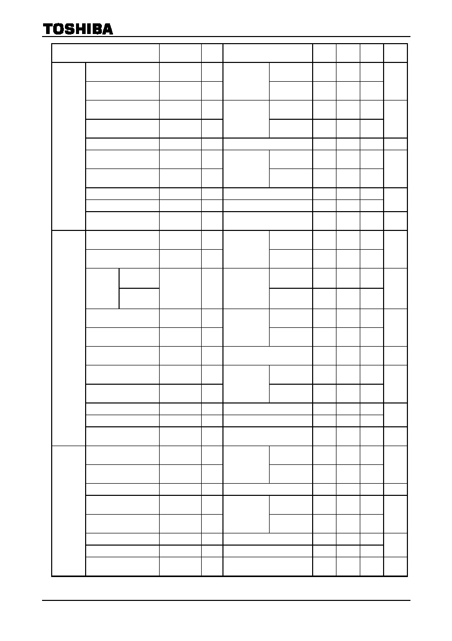
Pin Function
Pin No.
Symbol
I/O
Function Description
Remarks
1 V
CC
æ
Power supply input terminal.
æ
2 RFGC
I
RF amplitude adjustment control signal input terminal.
Controlled by 3-PWM signals.
(PWM carrier
=
88.2 kHz)
3 signals input.
(2VRO, VRO, GND)
3
GMAD
I
Open loop gain adjustment terminal for AGC amp.
(Note1)
4
FNI
I
Main beam I-V amp input terminal.
Connected to pin diode
output B
+
D
(through resistor).
5
FPI
I
Main beam I-V amp input terminal.
Connected to pin diode
output A
+
C
(through resistor).
6
TPI
I
Sub beam I-V amp input terminal.
Connected to pin diode
output F.
7
TNI
I
Sub beam I-V amp input terminal.
Connected to pin diode
output E.
8
MDI
I
Monitor photo diode amp input terminal.
Connected to monitor photo
diode.
9
LDO
O
Laser diode amp input terminal.
Connected to laser diode
control circuit.
10 SEL I
Laser diode control signal input terminal and APC circuit
ON/OFF control signal terminal.
SEL
Level
APC
Circuit
LDO
Detect
Frequency
GND OFF
Connected to V
CC
through resister (1 k
W
)
Low
HiZ
ON
Control signal output
Low
V
CC
ON
Control signal output
High
3 signals input.
(V
CC
, HiZ, GND)
11 TEB I
Tracking error balance adjustment signal input terminal.
Controlled by 3-PWM signal.
(PWM carrier
=
88.2 kHz)
3 signals input.
(2VRO, VRO, GND)
12 2VRO
O
Reference voltage (2VRO) output terminal.
2VRO
=
4.2 V when V
CC
=
5 V
æ
13
TEN
I
TE amp negative input terminal.
Connected to TEO through
feedback resistor.
14
TEO
O
TE error signal output terminal.
æ
15
SBAD
O
Sub beam adder signal output terminal.
æ
16
FEO
O
Focus error signal output terminal.
æ
17
FEN
I
FE amp negative input terminal.
Connected to FEO through
feedback resistor.
18 SEB I
RFRP output circuit switching terminal.
SEB Level
Bottom
Detection
Peak
Detection
GND ON ON
V
CC
OFF ON
Low (GND) is for normal use.
19 VRO
O
Reference signal (VRO) output terminal.
VRO
=
2.1 V when V
CC
=
5 V
æ
20
RFRP
O
Track count signal output terminal.
æ
21
BTC
I
Time constant adjustment terminal for bottom detection.
Adjusted by capacitance.
TA2153FN
2003-01-18
4
Pin No.
Symbol
I/O
Function Description
Remarks
22
RFCT
O
RFRP signal center level output terminal.
æ
23
PKC
I
Time constant adjustment terminal for peak detection.
Adjusted by capacitance.
24
RFRPIN
I
Input terminal for track count signal output amp.
æ
25
RFGO
O
Output terminal for RF signal amplitude adjustment amp.
æ
26 GVSW I
Amp (AGC, FE, TE) gain switching terminal.
GVSW Mode
GND CD-RW
HiZ Normal
V
CC
Normal
Low (GND) is for 5 times
gain.
27
AGCIN
I
Input terminal for RF signal amplitude adjustment amp.
Connected to RFO through
capacitance.
28
RFO
O
Output terminal for RF signal amp.
æ
29 GND
æ
Ground
terminal.
æ
30
RFN2
I
Input terminal for RF signal amp.
Connected to pin-diode
output A
+
B
+
C
+
D
(through resistor).
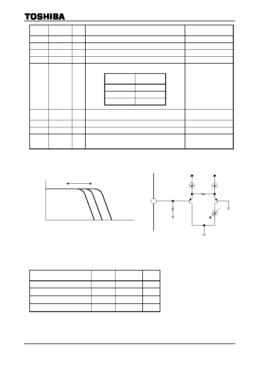
Note 1: Pin3 (GMAD) is gm adjustment terminal for AGC amp by applying a voltage (between 1.5 V and 4.2 V).
If pin3 (GMAD) is open, voltage of this terminal is fixed VR by IC interior.
Characteristic of frequency (open-loop characteristic) and voltage is as below.
Note 2: Current is changed by pin3 (GMAD) voltage.
Maximum Ratings
(Ta
=
=
=
=
25∞C)
Characteristics Symbol
Rating
Unit
Power supply voltage
V
CC
8 V
Power dissipation
P
D
500
mW
Operating temperature
T
opr
-
40~85 ∞C
Storage temperature
T
stg
-
55~150 ∞C
Gain
Frequency
GMAD Terminal Voltage
1.5 V
4.2 V
By changing a voltage (pin3) between 1.5 V and 4.2 V,
frequency band width is changed.
3
V
CC
VR
GMAD
(Note2)
VR
TA2153FN
2003-01-18
5
Electrical Characteristics
(unless otherwise specified, V
CC
=
=
=
=
5 V, Ta
=
=
=
=
25∞C)
Characteristics Symbol
Test
Circuit
Test Condition
Min
Typ.
Max
Unit
Assured power supply
voltage
V
CC
æ
æ
4.5 5.0 5.5 V
Power
supply
Power supply current
I
CC
æ
SEL
=
HiZ
26 35 44 mA
Reference voltage
2VR
æ
æ
4.0 4.2 4.4 V
Output current
I
OH2
æ
D
V
=
-
0.2 V
2.0
æ
æ
Reference
voltage
(2VRO)
Input current
I
OL2
æ
D
V
=
+
0.1 V
0.1
æ
æ
mA
Reference voltage
VR
æ
æ
2.0 2.1 2.2 V
Reference voltage limit
D
VR
æ
2
¥
VR/2VR
-
1
-
3.0 0 3.0 %
Output current
I
OH1
æ
D
V
=
-
0.2 V
5.0
æ
æ
Reference
voltage
(VRO)
Input current
I
OL1
æ
D
V
=
+
0.1 V
5.0
æ
æ
mA
Frequency band width
fc
æ
-
3dB point, R
IN
=
6 k
W
Between RFO
-
RFN2: 33 k
W
æ
8
æ
MHz
Output slew rate
SR
æ
C
RFO
=
20 pF, R
IN
=
6 k
W
Between RFO
-
RFN2: 33 k
W
æ
22
æ
V/
m
s
Output offset voltage
V
OS
æ
VR Reference
Between RFO
-
RFN2: 33 k
W
Input: VR short
æ
-
100
æ
mV
Upper limit output voltage
V
OH
æ
GND
Reference
3.8
æ
æ
Lower limit output voltage
V
OL
æ
GND
Reference
æ
æ
0.9
V
RF1
Permissive load
resistance
R
LM
æ
æ
10
æ
æ
k
W
Lower limit voltage gain 1
(normal mode)
Gv1L
æ
f
=
1 MHz, RFGC
=
0.6 V,
GVSW
=
V
CC
, GMAD
=
VR
0.6 0.7 0.8
Upper limit voltage gain 1
(normal mode)
Gv1H
æ
f
=
1 MHz, RFGC
=
3.6 V,
GVSW
=
V
CC
, GMAD
=
VR
1.3 1.5 1.7
Lower limit voltage gain 2
(CD-RW mode)
Gv2L
æ
f
=
1 MHz, RFGC
=
0.6 V,
GVSW
=
GND, GMAD
=
VR
2.7 3.2 3.6
Upper limit voltage gain 2
(CD-RW mode)
Gv2H
æ
f
=
1 MHz, RFGC
=
3.6 V,
GVSW
=
GND, GMAD
=
VR
5.8 6.8 7.7
V/V
Frequency band width
(normal mode)
fc1
æ
-
0.5dB point, RFGC
=
2.1 V,
GVSW
=
V
CC
, GMAD
=
VR
æ
12
æ
Frequency band width
(CD-RW mode)
fc2
æ
-
0.5dB point, RFGC
=
2.1 V,
GVSW
=
GND, GMAD
=
VR
æ
12
æ
MHz
Output slew rate
SR
æ
C
RFGO
=
20 pF
æ
40
æ
V/
m
s
Output offset voltage 1
(normal mode)
V
OS1
æ
GVSW
=
V
CC
æ
-
100
æ
Output offset voltage 2
(CD-RW mode)
V
OS2
æ
VR Reference
GMAD
=
VR
Input: Open
GVSW
=
GND
æ
0
æ
mV
Upper limit output voltage
V
OH
æ
GND
Reference
3.7
æ
æ
Lower limit output voltage
V
OL
æ
GND
Reference
æ
æ
0.9
V
RF2
(AGC)
Permissive load
resistance
R
LM
æ
æ
10
æ
æ
k
W
Voltage gain
Gv
æ
f
=
1 kHz
æ
200
æ
V/V
Operation ref. Voltage
V
MDI
æ
V
LDO
=
3.5 V
DC
170 178 192
mV
LD off voltage
V
LDOP
æ
SEL
=
GND, V
CC
Reference
-
0.7
æ
æ
V
APC
Input bias current
I
I
æ
MDI
=
178 mV
-
200
æ
200
nA
TA2153FN
2003-01-18
6
Characteristics Symbol
Test
Circuit
Test Condition
Min
Typ.
Max
Unit
Voltage gain 1
(normal mode)
Gv1
æ
GVSW
=
V
CC
4.3 4.8 5.3
Voltage gain 2
(CD-RW mode)
Gv2
æ
f
=
1 kHz
R
NF
=
91 k
W
R
FI
=
47 k
W
GVSW
=
GND
19.3 21.6 23.9
V/V
Gain balance 1
(normal mode)
GB1
æ
GVSW
=
V
CC
-
1.0
æ
1.0
Gain balance 2
(CD-RW mode)
GB2
æ
f
=
1 kHz
R
NF
=
91 k
W
R
FI
=
47 k
W
GVSW
=
GND
-
1.0
æ
1.0
dB
Frequency band width
fc
æ
-
3dB point
æ
26.5
æ
kHz
Output offset voltage 1
(normal mode)
V
OS1
æ
GVSW
=
V
CC
-
20
æ
20
Output offset voltage 2
(CD-RW mode)
V
OS2
æ
R
NF
=
91 k
W
R
FI
=
47 k
W
VR Reference
Input: VR short GVSW
=
GND
-
50
æ
50
mV
Upper limit output voltage
V
OH
æ
GND
Reference
3.8
æ
æ
Lower limit output voltage
V
OL
æ
GND
Reference
æ
æ
0.5
V
FE
Permissive load
resistance
R
LM
æ
æ
10
æ
æ
k
W
Voltage gain 1
(normal mode)
Gv1
æ
GVSW
=
V
CC
10.9 12.3 13.5
Voltage gain 2
(CD-RW mode)
Gv2
æ
f
=
1 kHz
R
FN
=
100 K
W
R
TI
=
47 k
W
GVSW
=
GND
50 56 60
V/V
max voltage
ratio
TEB
=
GND 40 45 50
Voltage
gain
adjustable
range
min voltage
ratio
D
Gv
æ
T
NI
input
TEB
=
VR
Reference
TEB
=
2VR
-
50
-
45
-
40
%
Gain balance 1
(normal mode)
GB1
æ
GVSW
=
V
CC
-
1.0
æ
1.0
Gain balance 2
(CD-RW mode)
GB2
æ
f
=
1 kHz
R
NF
=
100 k
W
R
FI
=
47 k
W
TEB
=
VR
GVSW
=
GND
-
1.0
æ
1.0
dB
Frequency characteristic
cut-off frequency
fc
æ
RNF
=
100 k
W
-
3dB point
æ
44
æ
kHz
Output offset voltage
(normal mode)
V
OS1
æ
GVSW
=
V
CC
-
80
æ
80
Output offset voltage
(CD-RW mode)
V
OS2
æ
R
NF
=
100 k
W
R
FI
=
47 k
W
VR Reference
Input: VR short GVSW
=
GND
-
300
æ
300
mV
Upper limit output voltage
V
OH
æ
GND
Reference
3.8
æ
æ
Lower limit output voltage
V
OL
æ
GND
Reference
æ
æ
0.5
V
TE
Permissive load
resistance
R
LM
æ
æ
10
æ
æ
k
W
Voltage gain 1
(normal mode)
Gv1
æ
GVSW
=
V
CC
2.0 2.7 3.4
Voltage Gain 2
(CD-RW mode)
Gv2
æ
f
=
1 kHz
R
TI
=
47 k
W
TEB
=
VR
GVSW
=
GND
9.0
12.2
15.3
V/V
Frequency Band Width
fc
æ
-
3dB point
æ
44
æ
kHz
Operation reference
voltage 1 (normal mode)
V
OPR1
æ
GVSW
=
V
CC
-
1.15
-
1.05
-
0.95
Operation reference
voltage 2 (CD-RW mode)
V
OPR2
æ
VR Reference
R
TI
=
47 k
W
Input: VR short GVSW
=
GND
-
1.0
-
0.9
-
0.8
V
Upper limit output voltage
V
OH
æ
GND
Reference
3.8
æ
æ
Lower limit output voltage
V
OL
æ
GND
Reference
æ
æ
1.3
V
SBAD
Permissive load
resistance
R
LM
æ
æ
10
æ
æ
k
W

TA2153FN
2003-01-18
7
Characteristics Symbol
Test
Circuit
Test Condition
Min
Typ.
Max
Unit
Voltage gain
Gv
æ
æ
æ
1.7
æ
V/V
Detection frequency
characteristic 1
fc1
æ
SEL
=
HiZ
æ
100
æ
Detection frequency
characteristic 2
fc2
æ
SEL
=
V
CC
æ
200
æ
kHz
Operation reference
voltage 1
V
OPR1
æ
VR Reference
No Input
-
1.1
-
1.0
-
0.9
Operation reference
voltage 2
V
OPR2
æ
VR Reference
700 kHz, 1.2 Vp-p
0.7 0.8 0.9
V
RFRP
Permissive load
resistance
R
LM
æ
æ
10
æ
æ
k
W
Detection frequency
characteristic 1
fc1
æ
C
BTC
=
0.22
m
F
æ
70
æ
Detection frequency
characteristic 2
fc2
æ
C
PKC
=
0.22
m
F
æ
70
æ
Hz
RFCT
RFRP
Æ
RFCT
Output offset voltage
V
OS
æ
RFRP Reference, RFCT
-
50
æ
50 mV
Note:
If the IC is used abnormally (ex. wrongly mounted), it may be damaged or destroyed.

TA2153FN
2003-01-18
8
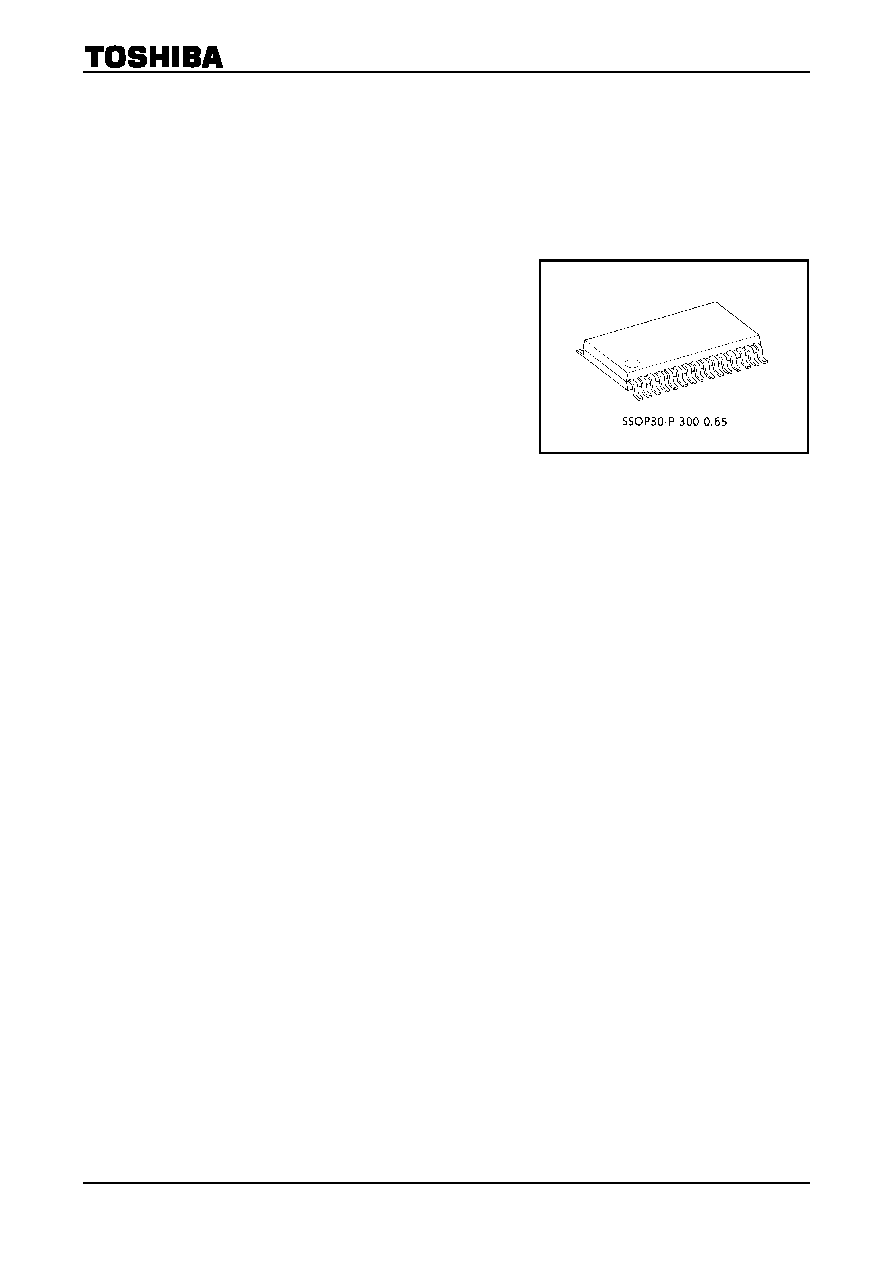
Package Dimensions
Weight: 0.17 g (typ.)

TA2153FN
2003-01-18
9
∑
TOSHIBA is continually working to improve the quality and reliability of its products. Nevertheless, semiconductor
devices in general can malfunction or fail due to their inherent electrical sensitivity and vulnerability to physical
stress. It is the responsibility of the buyer, when utilizing TOSHIBA products, to comply with the standards of
safety in making a safe design for the entire system, and to avoid situations in which a malfunction or failure of
such TOSHIBA products could cause loss of human life, bodily injury or damage to property.
In developing your designs, please ensure that TOSHIBA products are used within specified operating ranges as
set forth in the most recent TOSHIBA products specifications. Also, please keep in mind the precautions and
conditions set forth in the "Handling Guide for Semiconductor Devices," or "TOSHIBA Semiconductor Reliability
Handbook" etc..
∑
The TOSHIBA products listed in this document are intended for usage in general electronics applications
(computer, personal equipment, office equipment, measuring equipment, industrial robotics, domestic appliances,
etc.). These TOSHIBA products are neither intended nor warranted for usage in equipment that requires
extraordinarily high quality and/or reliability or a malfunction or failure of which may cause loss of human life or
bodily injury ("Unintended Usage"). Unintended Usage include atomic energy control instruments, airplane or
spaceship instruments, transportation instruments, traffic signal instruments, combustion control instruments,
medical instruments, all types of safety devices, etc.. Unintended Usage of TOSHIBA products listed in this
document shall be made at the customer's own risk.
∑
The products described in this document are subject to the foreign exchange and foreign trade laws.
∑
The information contained herein is presented only as a guide for the applications of our products. No
responsibility is assumed by TOSHIBA CORPORATION for any infringements of intellectual property or other
rights of the third parties which may result from its use. No license is granted by implication or otherwise under
any intellectual property or other rights of TOSHIBA CORPORATION or others.
∑
The information contained herein is subject to change without notice.
000707EBA
RESTRICTIONS ON PRODUCT USE