 | –≠–ª–µ–∫—Ç—Ä–æ–Ω–Ω—ã–π –∫–æ–º–ø–æ–Ω–µ–Ω—Ç: TA8132 | –°–∫–∞—á–∞—Ç—å:  PDF PDF  ZIP ZIP |

TA8132AN / AF , TA2012N / F
2002-10-30
1
TOSHIBA Bipolar Linear Integrated Circuit Silicon Monolithic
TA8132AN,TA8132AF,TA2012N,TA2012F
3V AM / FM IF + MPX
(For Digital Tuning System)
TA8132AN, TA8132AF and TA2012N, TA2012F are the AM / FM
IF+ST DET system ICs, which are designed for DTS radios.
These are included many functions and these can be used for
digital tuning system with IF counter.
Features
∑ Built-in AM / FM IF and FM stereo PLL multiplex decoder.
∑ Suitable for combination with digital tuning system which is
included IF counter.
One terminal type AM / FM IF count output (auto stop
signal) for IF counter of digital tuning system.
FM: 10.7MHz or 1.3375MHz (1 / 8 dividing)
changeable by external switch
AM: 450kHz
Built-in mute circuit for IF count output.
It is controlled by the IF request signal from digital
tuning system,
Pin(8) level: High come out
Low non output
Adjustable for IF count output sensitivity by external
resistance of pin(2).
∑ For adopting ceramic discriminator and ceramic resonator, it
is not necessary to adjust the FM quad detector circuit and
FM ST DET VCO circuit.
∑ S curve characteristics of FM detection output in TA8132AN, TA8132AF and TA2012N, TA2012F are reverse to
each other.
TA8132AN, TA8132AF: Reverse characteristic.
TA2012N, TA2012F: Normal characteristic.
∑ Built-in one terminal type AM low cut circuit.
∑ TA2053F is reverse pin type of TA2012F.
∑ Operating supply voltage range (Ta = 25∞C)
V
CC (opr.)
= 1.8~8.0V
Weight
SDIP24-P-300-1.78: 1.2g (typ.)
SSOP24-P-300-1.00 : 0.31g (typ.)

TA8132AN / AF , TA2012N / F
2002-10-30
2
Block Diagram
(Note)
We recommend
Ceramic resonator: CSB456F18
Ceramic discriminator: CDA10.7MG18 (MURATA MFG CO., LTD)

TA8132AN / AF , TA2012N / F
2002-10-30
3
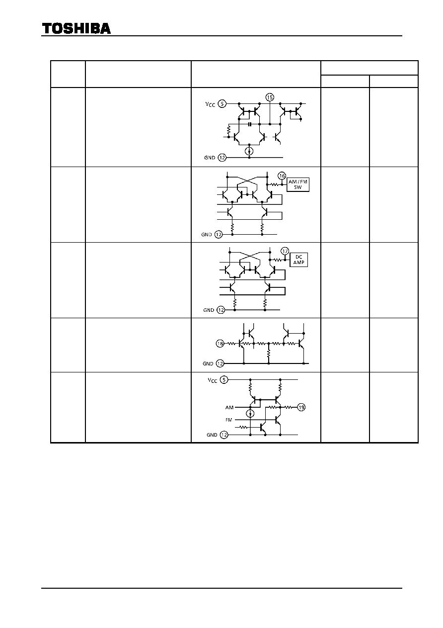
Explanation Of Terminals
DC Voltage (V)
(at no Signal)
Pin
No.
Item Internal
Circuit
AM FM
1 AM
RF
IN
3.0 3.0
2
IF count output sensitivity adjust
terminal
FM IF divider control terminal
3 AM
OSC
3.0 3.0
4 AM
OSC
OUT
2.7 3.0
5 V
CC
3.0 3.0
6 AM
LOW
CUT
2.3 2.3

TA8132AN / AF , TA2012N / F
2002-10-30
4
DC Voltage (V)
(at no Signal)
Pin
No.
Item Internal
Circuit
AM FM
7 AGC
0.25 0.35
8 IF
OUT
SW
9 IF
OUT
3.0 3.0
10
TUN LED (tuning LED)
11
ST LED (stereo LED)
12 GND
0 0
13
14
R
-OUT
L
-OUT
1.0 1.0
TA8132AN / AF , TA2012N / F
2002-10-30
5
DC Voltage (V)
(at no Signal)
Pin
No.
Item Internal
Circuit
AM FM
15 VCO
2.5
2.5
(VCO
stop
mode)
16
LPF2
LPF terminal for synchronous
detector
Bias terminal for AM / FM switch
circuit
V
16
= V
CC
AM
V
16
= openFM
3.0 2.2
17
LPF1
LPF Terminal for phase detector
VCO stop terminal
V
17
= V
CC
VCO stop
2.7 2.2
18
FM ST DET IN
0.7 0.7
19 DET
OUT
1.1 1.1

TA8132AN / AF , TA2012N / F
2002-10-30
6
DC Voltage (V)
(at no Signal)
Pin
No.
Item Internal
Circuit
AM FM
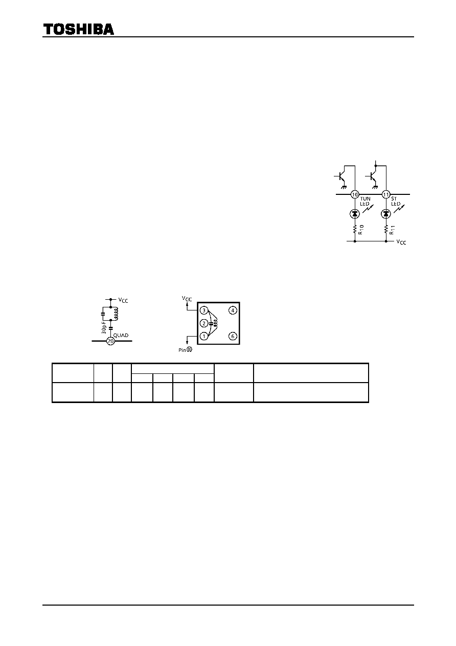
20
QUAD (FM QUAD. Detector)
2.4 2.1
21
AM IF IN
3.0 3.0
22
BY
-PASS
By
-pass for AM/FM IF AMP
2.3 2.8
23
AM MIX OUT
3.0 3.0
24 FM
IF
IN
3.0 3.0

TA8132AN / AF , TA2012N / F
2002-10-30
7
Application Note
1. How to control the IF count output signal (pin(9) output)
TUN LED
ON OFF
H
Come out
Non output
V
8
L
Non output
Non output
∑ Whether or not there is the IF count output signal (pin(9) output) is determined by the and of the pin(8)
control voltage: V
8
and tuning LED on / off switching.
In the condition of
V
8
: High (active high, V
TH
= 0.8V (typ.))
TUN LED: ON (V
in
V
L
+2dBµV EMF (typ.))
the IF count output signal comes out from the pin(9).
In the case of the tuning LED function is not needed, it doesn't matter the pin(10) is opened.
∑ The output impedance of pin(9) is 1.5k (typ.) (cf.P.4)
It is possible to reduce the IF count output signal level to add the resistance between the pin(9) and the V
CC
line.
∑ The signal waveform is the rectangular wave, and the level is 500mV
p-p
(typ.)
2. How to control the divider of FM IF
Switch
V
CC
: 10.7MHz output
GND or OPEN: 1.3375MHz output (1 / 8 dividing)
3. How to adjust the IF count output sensitivity
∑ The IF count output sensitivity (search sensitivity)
Can be adjusted by varying the IF AMP gain for FM and varying the MIXER gain for AM.
This setting is made by changing the value of external resistance R
2
which is connected to
pin(2).
∑ However, this is only possible at the auto-tuning mode. (external voltage supplied to pin(8) is at high level.)
The original again returns while receiving a broadcast station (supplied voltage to pin(8) is at low level.)

TA8132AN / AF , TA2012N / F
2002-10-30
8
∑ The gain loss of FM IF AMP
R2
0 10K (Note)
IF
(10.7MHz)
-20dB
-1dB
M
ode
1 / 8 IF
(1.3375MHz)
-20dB
-1dB
(Note)
In the condition of the 1 / 8 IF mode, it is
possible to set up R
2
= (OPEN).
In the condition of IF mode, it is necessary to set up the value of R
2
under 10k. When the R
2
is over
10k it is feared that the mode is change to the 1 / 8 IF mode.
∑ The gain loss of AM MIXER
R2
0 10K
-16dB
-1dB
4. AM low-cut circuit
∑ The AM low-cut action is carried out by the bypass of the high frequency component of
the positive-feedback signal at the AF AMP stage. The external capacitor: C
6
by-passes this component.
∑ The cut-off frequency f
L
is determine by the internal resistance 22k (typ.) and the
external capacitor C
6
as following;
(Hz)
6
C
3
10
22
2
1
L
f
¥
¥
¥
p
¥
=
∑ In the case of the AM low-cut function is not needed, set up the value of C
6
over 0.47µF.
In the condition of C
6
0.47µF, the frequency characteristic has flat response at the low frequency.
TA8132AN / AF , TA2012N / F
2002-10-30
9
5. AM local oscillator buffer output
∑ The output impedance of AM local oscillator buffer output pin (pin(4)) is 750 (typ.) (cf.P.3)
∑ It is possible to reduce the output level to add the resistance between the pin(4) and V
CC
line. The signal
waveform is the rectangular wave, and the level is 500mV
p-p
(f
OSC
= 1.45MHz, typ.)
∑ The higher local oscillation frequency (f
OSC
) to be, the lower buff output level to be owing to the load capacity.
So, in the case that it is connected to other circuits, take care of the input capacity of these circuits and stray
capacity of wire.
6. Tuning LED driver and stereo LED driver
∑
The tuning LED driver and stereo LED driver don't have current limit resistance
shown in the right figure. So, it is necessary to add the current limit resistance:
R
10
, R
11.
∑ Set up the values of R
10
, R
11
to keep the drive currents ID10, ID11 under 10mA.
7.FM detection circuit
For the FM detection circuit,detection coil is able to use instead of ceramic discriminator.
Recommended circuit and recommended coil are as follows.
In this case, please take care that V
in
(lim.)
falls a little.
Turns
Test
Frequency
C
o
(pF)
Q
o
1
-2 2-3 1-3 4-6
Wire
(mm
f)
REF
10.7MHz 100
100
12
0.12 UEW
SUMIDA ELECTRIC CO., LTD
2153
-4095-189 or equivalent

TA8132AN / AF , TA2012N / F
2002-10-30
10
8. FM / AM switch and forced monaural switch
FM / AM switch over and stere / forced monaural switch over are done by
internal PNP transistors ON / OFF which are connected to pin(16) and pin
(17) respectively.
The threshold voltages of these PNP transistors are V
th
= V
CC,
and for
switching, we recommend to use mechanical switch.
(Direct short to V
CC
line.)
In the case of the electrical switch over by transistor, set up V
CE
(saturation voltage between collector and emitter) 50mV or less, otherwise
there are some cases that it does not become the AM mode and force
monaural mode.
When these external switches are ON, the currents which flow into pin(16)
and pin(17) are 100µA and 20µA respectively. (Typical value at V
CC
= 3V)
Maximum Ratings
(Ta = 25∞C)
Characteristic Symbol
Rating
Unit
Supply voltage
V
CC
8 V
LED current
I
LED
10
mA
LED voltage
V
LED
8 V
TA8132AN 1200
Power dissipation
TA8132AF
PD (Note)
400
mW
Operating Temperature
T
opr
-25~75
∞C
Storage temperature
T
stg
-55~150 ∞C
(Note): Derated above 25∞C in the proportion of 9.6mW / ∞C for TA8132AN, TA2012N and
of 3.2mW / ∞C for TA8132AF, TA2012F.

TA8132AN / AF , TA2012N / F
2002-10-30
11
Electrical characteristics
Unless Otherwise Specified, Ta = 25∞C, V
CC1
= 3V, SW
1
10k, SW
3
OFF
FM IF: f = 10.7MHz, f = ±22.5kHz, f
m
= 1kHz
AM: f = 1MHz, MOD = 30%, f
m
= 1kHz
MPX:
f
m
= 1kHz
Characteristic Symbol
Test
Cir
-
cuit
Test Condition
Min.
Typ.
Max.
Unit
I
CC
(FM)
1
FM mode, V
in
= 0
11.0 14.0
Supply current
I
CC
(AM)
1
AM mode, V
in
= 0
10.5 13.5
mA
Input limiting
voltage
V
in (lim.)
1
-3dB limiting point
41
46
51
dBµV
EMF
Recovered output
voltage
V
OD
1
V
in
= 80dBµV EMF
50
75
100
mV
rms
Signal to noise
ratio
S / N
1
V
in
= 80dBµV EMF
65 dB
Total harmonic
distortion
THD 1
V
in
= 80dBµV EMF
0.2
%
AM rejection ratio
AMR
1
V
in
= 80dBµV EMF
38
dB
LED on sensitivity
V
L
1
I
L
=
1mA
48 53 58
dBµV
EMF
IF f
IF
(FM)
1
V
in
= 80dBµV EMF,
SW
2
V
CC,
SW
3
ON
10.7
IF count
output
frequency
1 / 8 IF
f
1 / 8 IF
(FM)
1
V
in
= 80dBµV EMF,
SW
2
GND
,
SW
3
ON
1.3374 1.3375 1.3376
MHz
IF V
IF
(FM)
1
V
in
= 61dBµV EMF,
SW
2
V
CC,
SW
3
ON
350 500
IF count
output
voltage
1 / 8 IF
V
1 / 8 IF
(FM)
1
V
in
= 61dBµV EMF,
SW
2
GND
,
SW
3
ON
350 500
mV
p
-p
SW
1
0
,
SW
2
GND,
SW
3
ON
76
SW
1
510,
SW
2
GND,
SW
3
ON
68
SW
1
0
,
SW
2
,V
CC,
SW
3
ON
77
FM
IF
IF count output
sensitivity
IF
sens. (FM)
1
SW
1
510
,
SW
2
,V
CC,
SW
3
ON
69
dBµV
EMF

TA8132AN / AF , TA2012N / F
2002-10-30
12
Characteristic Symbol
Test
Cir
-
cuit
Test Condition
Min.
Typ.
Max.
Unit
Gain
V
1
V
in
= 26dBµV EMF
28
57
85
Recovered output
voltage
V
OD
1
V
in
= 60dBµV EMF
50
75
100
mV
rms
Signal to noise
ratio
S / N
1
V
in
= 60dBµV EMF
41
dB
Total harmonic
distortion
THD 1
V
in
= 60dBµV EMF
1.0
%
LED on sensitivity
V
L
1
I
L
=
1mA
21 26 31
dBµV
EMF
1 f
OSC
= 1.45MHz
350
500
Local OSC buff.
output voltage
V
OSC
(AM)
2 f
OSC
= 27MHz
500
mV
p
-p
IF count output
voltage
V
IF
(AM) 1
V
in
= 39dBµV EMF, SW
3
ON 350
500
mV
p
-p
SW
1
0
,
SW
2
GND,
SW
3
ON
49
SW
1
510,
SW
2
GND,
SW
3
ON
42
SW
1
0
,
SW
2
,V
CC,
SW
3
on
49
AM
IF count output
sensitivity
IF
sens. (AM)
1
SW
1
510
,
SW
2
,V
CC,
SW
3
ON
42
dBµV
EMF
FM mode
0.6
Pin(19) output resistance
R
19
1
AM mode
12
k

TA8132AN / AF , TA2012N / F
2002-10-30
13
Characteristic Symbol
Test
Cir
-
cuit
Test Condition
Min.
Typ.
Max.
Unit
Input resistance
R
IN
1
25
Output resistance
R
OUT
1
5
k
Max. composite
signal input voltage
V
in MAX
(stereo)
1
L + R = 90%, P = 10%
THD = 3%, SW
9
LPF: ON
350 mV
rms
f
m
= 100kHz
42
f
m
= 1kHz
35
42
Separation Sep
L + R = 135mV
rms
P = 15mV
rms
,
SW
9
LPF: ON
f
m
= 10kHz
42
dB
Monaural
THD
(monaural)
V
in
= 150 mV
rms
(mono)
0.2
Total
harmonic
distortion Stereo
THD
(stereo)
1
L + R = 135mV
rms
,
P = 15mV
rms
SW
9
LPF: ON
0.2
%
Voltage gain
G
V
(MPX) 1
V
in
= 150mV
rms
(mono)
-5
-3
-1 dB
Channel balance
C.B.
1
V
in
= 150mV
rms
(mono)
-2 0 2 dB
ON V
L
(ON)
8 15
Stereo LED
sensitivity
OFF V
L
(OFF)
1 Pilot
input
2 6
mV
rms
Stereo LED hysteresis
V
H
1
To LED turn off from
LED turn on
2 mV
rms
Capture range
C.R.
1
P = 15mV
rms
±1.3 %
MP X
Signal to noise ratio
S / N
1
V
in
= 150mV
rms
(mono)
78 dB

TA8132AN / AF , TA2012N / F
2002-10-30
14
Test Circuit 1
Coil Data
(test circuit 1)
Turn
Coil No.
f
L
(µH)
C
o
(pF)
Q
o
1
-2
2
-3
1
-3
4
-6
Wire
(mm)
RED. (Coil No.)
T
1
AM OSC
796kHz
288
115
13 73
0.08 UEW 4147
-1356-038 (S)
T
2
AM IFT
455KHz
180
120
180
15
0.06 UEW 2150
-2162-165 (S)
(S): SUMIDA ELECTRIC Co., Ltd.

TA8132AN / AF , TA2012N / F
2002-10-30
15
Test Circuit 2
Coil Data
(test circuit 2)
Turn
Coil No.
f
L
(µH)
C
o
(pF)
Q
o
1
-2
2
-3
1
-3
4
-6
Wire
(mm)
REF. (Coil No.)
T
AM OSC
7.96MHz
1.4
84
1 6 7
0.08 UEW (T) 7PL
-1344Y
(T): TOKO Co., Ltd.

TA8132AN / AF , TA2012N / F
2002-10-30
16

TA8132AN / AF , TA2012N / F
2002-10-30
17

TA8132AN / AF , TA2012N / F
2002-10-30
18

TA8132AN / AF , TA2012N / F
2002-10-30
19
Package Dimensions
Weight: 1.2g (typ.)

TA8132AN / AF , TA2012N / F
2002-10-30
20
Package Dimensions
Weight: 0.31g (typ.)

TA8132AN / AF , TA2012N / F
2002-10-30
21
∑ TOSHIBA is continually working to improve the quality and reliability of its products. Nevertheless, semiconductor
devices in general can malfunction or fail due to their inherent electrical sensitivity and vulnerability to physical
stress. It is the responsibility of the buyer, when utilizing TOSHIBA products, to comply with the standards of
safety in making a safe design for the entire system, and to avoid situations in which a malfunction or failure of
such TOSHIBA products could cause loss of human life, bodily injury or damage to property.
In developing your designs, please ensure that TOSHIBA products are used within specified operating ranges as
set forth in the most recent TOSHIBA products specifications. Also, please keep in mind the precautions and
conditions set forth in the "Handling Guide for Semiconductor Devices," or "TOSHIBA Semiconductor Reliability
Handbook" etc..
∑ The TOSHIBA products listed in this document are intended for usage in general electronics applications
(computer, personal equipment, office equipment, measuring equipment, industrial robotics, domestic appliances,
etc.). These TOSHIBA products are neither intended nor warranted for usage in equipment that requires
extraordinarily high quality and/or reliability or a malfunction or failure of which may cause loss of human life or
bodily injury ("Unintended Usage"). Unintended Usage include atomic energy control instruments, airplane or
spaceship instruments, transportation instruments, traffic signal instruments, combustion control instruments,
medical instruments, all types of safety devices, etc.. Unintended Usage of TOSHIBA products listed in this
document shall be made at the customer's own risk.
∑ The products described in this document are subject to the foreign exchange and foreign trade laws.
∑ The information contained herein is presented only as a guide for the applications of our products. No
responsibility is assumed by TOSHIBA CORPORATION for any infringements of intellectual property or other
rights of the third parties which may result from its use. No license is granted by implication or otherwise under
any intellectual property or other rights of TOSHIBA CORPORATION or others.
∑ The information contained herein is subject to change without notice.
000707EBA
RESTRICTIONS ON PRODUCT USE