 | –≠–ª–µ–∫—Ç—Ä–æ–Ω–Ω—ã–π –∫–æ–º–ø–æ–Ω–µ–Ω—Ç: TA8233BH | –°–∫–∞—á–∞—Ç—å:  PDF PDF  ZIP ZIP |

TA8233BH
2002-10-30
1
TOSHIBA Bipolar Linear Integrated Circuit Silicon Monolithic
TA8233BH
30W BTL ◊ 2ch Audio Power Amplifier
The thermal resistance j-T of TA8233BH package designed for
low thermal resistance, has high efficiency of heat radiation.
The temperature rise of chip can be reduced, and the influence
from the degradation of the features due to the temperature rise
at the high output can also be reduced.
This stereo audio power IC, designed for car audio use, has two
built-in channels to reduce the characteristic difference between
L and R channels. It also contains output short detection circuit,
output clip detection and various kind of protection.
Features
∑ High power
: P
OUT (1)
= 30W (typ.) / channel
(V
CC
= 14.4V, f = 1kHz, THD = 10%, R
L
= 2)
P
OUT (2)
= 26W (typ.) / channel
(V
CC
= 13.2V, f = 1kHz, THD = 10%, R
L
= 2)
P
OUT (3)
= 19W (typ.) / channel
(V
CC
= 13.2V, f = 1kHz, THD = 10%, R
L
= 4)
∑ Low thermal resistance: j-T = 1.5∞C / W (infinite heat sink)
∑ Low distortion ratio: THD = 0.04% (typ.)
(V
CC
= 13.2V, f = 1kHz, P
OUT
= 1W, R
L
= 4, G
V
= 50dB)
∑ Low noise: V
NO
= 0.30mV
rms
(typ.)
(V
CC
= 13.2V, R
L
= 4, G
V
= 50dB, R
g
= 0, BW = 20Hz~20kHz)
∑ Built-in stand-by function
: (with pin(4) set at low, power is turned off.) I
SB
= 1µA (typ.)
∑ Built-in output clip detection circuit
:
(pin(1): Open collector (active low))
∑ Built-in output short detection circuit
: (pin(9): Open collector (active low))
∑ Built-in various protection circuits
: Thermal shut down, Over voltage, OutV
CC
short, OutGND short and Out-Out short.
∑ Operating supply voltage: V
CC (opr)
= 9~18V
Weight: 9.8g (typ.)

TA8233BH
2002-10-30
2
Block Diagram
TA8233BH (G
V
= 50dB)
Caution And Application Method
(description is made only on the single channel.)
1. Voltage gain adjustment
This IC has the amplifier constructions as shown in Fig.1. The pre-amp (amp 1) is provided to the primary
stage, and the input voltage is amplified by the flat amps, amp 3 and amp 4 of each channel through the phase
amp (amp 2).
Since the input offset is prevented by pre-amp when V
CC
is set to on, this circuit can remarkably reduce the pop
noise.

TA8233BH
2002-10-30
3
The total closed loop gain G
V
of this IC can be obtained by expression below when the closed loop voltage gain of
amp 1 is G
V1
.
(1)
(dB)
R2
f
R
R2)
f
(R
R1
og
20
V1
G
L
L
L
l
+
+
+
=
The closed loop voltage gain of power amp, amp 3 and
amp 4 is fixed at G
V3
G
V4
= 20dB.
Therefore, the total closed circuit voltage gain G
V
is
obtained through BTL connection by the expression as
below.
G
V
= G
V1
+ G
V3
+ 6 (dB).........(2)
For example, when R
f
= 0, G
V
is obtained by the
expressions (1) and (2) as below.
G
V
24 + 20 + 6 = 50dB
The voltage gain is reduced when R
f
is increased.
(Fig.2)
With the voltage gain reduced, since (1) the oscillation
stability is reduced, and (2) the pop noise changes
when V
CC
is set to on, refer to the items 3 and 4.
2. Stand-by SW function
By means of controlling pin(4) (stand-by terminal) to
high and low, the power supply can be set to on and off.
The threshold voltage of pin(4) is set at 2.1V (3V
BE
), and
the power supply current is about 1µA (typ.) at the
stand-by state.
Control voltage of pin(4): V
(SB)
Stand
-By Power V
(SB)
(V)
On Off 0~2
Off On
3~V
CC
Adjustage of stand-by SW
(1) Since V
CC
can directly be controlled to on or off by the microcomputer, the switching relay can be omitted.
(2) Since the control current is microscopic, the switching relay of small current capacity is satisfactory for
switching

TA8233BH
2002-10-30
4
3. Preventive measure against oscillation
For preventing the oscillation, it is advisable to use C4, the condenser of polyester film having small
characteristic fluctuation of the temperature and the frequency.
The condenser (C6) between input and GND is effective for preventing oscillation which is generated with a
feedback signal from a output stage.
The resistance R to be series applied to C4 is effective for phase correction of high frequency, and improves the
oscillation allowance.
(1) Voltage gain to be used (G
V
setting)
(2) Capacity value of condenser
(3) Kind of condenser
(4) Layout of printed board
In case of its use with the voltage gain G
V
reduced or with the feedback amount increased, care must be taken
because the phase-inversion is caused by the high frequency resulting in making the oscillation liable
generated.
4. Adjustment of output offset (when the power supply turn on)
As this IC is constructed with DC circuit on the pre-amp stage, it is necessary to lower a input offset or output
offset by agreement with the each leading edge time constant of the input voltage in the pre-amp stage and NF
terminal voltage.
Concretely, monitor the output DC voltage and vary the capacity value in input condenser and NF condenser
(see Fig.4)
(Reference) In case of setting the condition (G
V
= 40dB) with R
f
= 470

TA8233BH
2002-10-30
5
5. Output clip detection function (pin(1))
The output clip detection terminal of pin(1) has the open collector output structure on chip as shown in Fig.5. In
case that the output waveform is clipping, the clip detection circuit is operated and NPN Tr. is turned on.
It is possible to improve the tone quality with the current of flowing into pin(1) and with controlling the volume,
tone control circuit through L.P.F smoothing circuit as shown in Fig.5.
In case of being unused this function, use this IC as open connection on pin(1).
(Application)

TA8233BH
2002-10-30
6
6. Output to V
CC
, output to gnd short detection function (pin(9))
The output short detection terminal of pin(9) has open collector output structure on chip as shown in Fig.6.
In unusual case that output terminal of power amp. Is condition of output to V
CC
or output to GND short, it is
possible to protect all the system of apparatus as well as power IC protection.
In case of being unused this function, use this IC as open-connection on pin(9).
(Application)
7. Rapid ripple discharging circuit at the time of V
CC
off
This circuit is effective in such a mode where the V
CC
and the stand-by terminals become high or low
simultaneously; for instance, for a pop noise produced when the power is turned on or off repeatedly by
operating the ignition key.
When V
CC
is off, this detection circuit detect V
CC
8V internally on IC.
(1) The power stage bias circuit is cut.
(2) pin(8): Ripple capacitor is rapidly discharged by turning Q3 on and then Q1 and Q2 on.

TA8233BH
2002-10-30
7
(Precaution
1)
When the stand-by terminal was put to the low level after the ripple rapid discharging circuit was operated
(V
CC
8V) at the time when V
CC
was turned off, a pop noise may be generated. Therefore, V
CC
which makes
the stand-by terminal low shall be set at 8V or above so that (1) the stand-by terminal is put at the low level
and (2) the ripple rapid discharging circuit is turned on when V
CC
is turned off (in order of (1) and (2)). An
example of application is shown in Fig.9.
(Precaution 2)
If the falling time constant of the V
CC
line is large (the fall is gentle), the pop noise may become worse.
In this case, it is possible to prevent the pop noise from becoming worse by reducing the ability of "ripple rapid
discharging circuit at the time of V
CC
off" according to the increase of the capacity of ripple capacitor of pin(8).
However, it shall be kept in mind that the time for turning the power on becomes longer as the result of this
method.
8. External part list and description
Influence
Sym
-
bol
Recommended
Value
Feature
Smaller Than
Recommended Value
Larger Than
Recommended Value
Remarks
C1
4.7µF
DC blocking
Related to pop noise at V
CC
on.
Related to gain.
Refer to item 4.
Related to pop noise at V
CC
on.
C2 47µF
Feedback
condenser
Determination of low cut
-off frequency
f
R
L
f
2
1
C2
◊
◊
p
=
C3 220µF
Ripple
reduction Time constant is small
at V
CC
on or off.
Time constant is large
at V
CC
on or off.
C4
0.12µF
Oscillation prevention Made liable to oscillate.
Oscillation allowance
Refer to item 3.
C5 1000µF
Ripple
filter
For filtering power supply hum and ripple.
Large at using AC rectified power supply.
Small at using DC power supply.
C6 1000pF
Oscillation
prevention
Oscillation allowance improved.
Noise reduction
Refer to item 3.
TA8233BH
2002-10-30
8
Maximum Ratings
(Ta = 25∞C)
Characteristic Symbol
Rating
Unit
Peak supply voltage (0.2s)
V
CC (surge)
50 V
DC supply voltage
V
CC (DC)
25 V
Operating supply voltage
V
CC (opr)
18 V
Output current (peak)
I
O (peak)
9 A
Power dissipation
P
D
50
W
Operating temperature
T
opr
-30~85 ∞C
Storage temperature
T
stg
-55~150 ∞C
Electrical Characteristics
(unless otherwise specified, V
CC
= 13.2V, R
L
= 4
,
f = 1kHz, Ta = 25∞C)
Characteristic Symbol
Test
Cir
-
cuit
Test Condition
Min.
Typ.
Max.
Unit
Quiescent supply current
I
CCQ
--
V
IN
= 0
--
120
250
mA
P
OUT
(1)
--
V
CC
= 14.4V, R
L
= 2
THD = 10%
-- 30 --
P
OUT
(2)
--
R
L
= 2, THD = 10%
17
26
--
Output power
P
OUT
(3)
--
THD = 10%
16
19
--
W
Total harmonic distortion
ratio
THD --
P
OUT
= 1W
--
0.04
0.4
%
Voltage gain
G
V
--
--
48 50 52 dB
Voltage gain ratio
G
V
--
--
-1.0 0 1.0 dB
Output noise voltage
V
NO
--
R
g
= 0, BW = 20Hz~20kHz
--
0.3
0.7
mV
rms
Ripple rejection ratio
R.R.
--
f
ripple
= 100Hz, R
g
= 600
40 54 -- dB
Input resistance
R
IN
--
--
--
30
--
k
Output offset voltage
V
offset
--
V
IN
= 0
-100 0 100
mV
Current at stand
-by state
I
SB
--
--
--
1
10
µA
Cross talk
C.T.
--
R
g
= 600
V
OUT
= 0.775V
rms
(0dBm)
-- 60 -- dB
Pin(4) control voltage
V
SB
--
Stand
-byoff
(poweron)
2.5 -- V
CC
V
Pin(1) (clip DET)
saturation voltage
V
sat (1)
--
I
C
=
1mA
-- 100 -- mV
Pin(9) (short DET)
saturation voltage
V
sat (9)
--
I
C
=
1mA
-- 100 -- mV
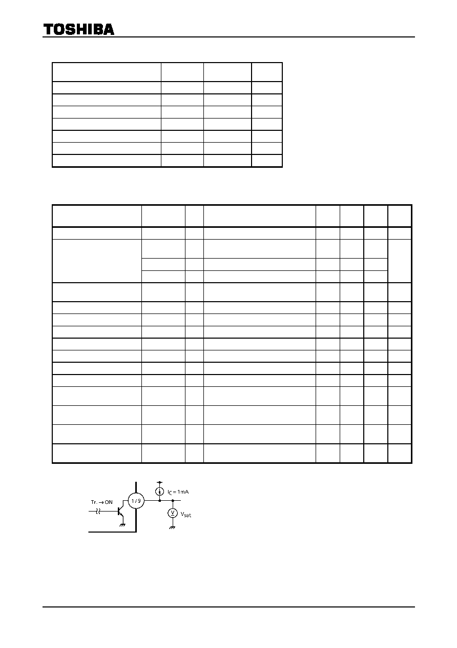
V
sat (1)
, V
sat (9)
Test Circuit

TA8233BH
2002-10-30
9
Test Circuit
TA8233BH (G
V
= 50dB)

TA8233BH
2002-10-30
10

TA8233BH
2002-10-30
11

TA8233BH
2002-10-30
12

TA8233BH
2002-10-30
13
Package Dimensions
Weight: 9.8g (typ.)

TA8233BH
2002-10-30
14
∑ TOSHIBA is continually working to improve the quality and reliability of its products. Nevertheless, semiconductor
devices in general can malfunction or fail due to their inherent electrical sensitivity and vulnerability to physical
stress. It is the responsibility of the buyer, when utilizing TOSHIBA products, to comply with the standards of
safety in making a safe design for the entire system, and to avoid situations in which a malfunction or failure of
such TOSHIBA products could cause loss of human life, bodily injury or damage to property.
In developing your designs, please ensure that TOSHIBA products are used within specified operating ranges as
set forth in the most recent TOSHIBA products specifications. Also, please keep in mind the precautions and
conditions set forth in the "Handling Guide for Semiconductor Devices," or "TOSHIBA Semiconductor Reliability
Handbook" etc..
∑ The TOSHIBA products listed in this document are intended for usage in general electronics applications
(computer, personal equipment, office equipment, measuring equipment, industrial robotics, domestic appliances,
etc.). These TOSHIBA products are neither intended nor warranted for usage in equipment that requires
extraordinarily high quality and/or reliability or a malfunction or failure of which may cause loss of human life or
bodily injury ("Unintended Usage"). Unintended Usage include atomic energy control instruments, airplane or
spaceship instruments, transportation instruments, traffic signal instruments, combustion control instruments,
medical instruments, all types of safety devices, etc.. Unintended Usage of TOSHIBA products listed in this
document shall be made at the customer's own risk.
∑ This product generates heat during normal operation. However, substandard performance or malfunction may
cause the product and its peripherals to reach abnormally high temperatures.
The product is often the final stage (the external output stage) of a circuit. Substandard performance or
malfunction of the destination device to which the circuit supplies output may cause damage to the circuit or to the
product.
∑ The products described in this document are subject to the foreign exchange and foreign trade laws.
∑ The information contained herein is presented only as a guide for the applications of our products. No
responsibility is assumed by TOSHIBA CORPORATION for any infringements of intellectual property or other
rights of the third parties which may result from its use. No license is granted by implication or otherwise under
any intellectual property or other rights of TOSHIBA CORPORATION or others.
∑ The information contained herein is subject to change without notice.
000707EBF
RESTRICTIONS ON PRODUCT USE