 | –≠–ª–µ–∫—Ç—Ä–æ–Ω–Ω—ã–π –∫–æ–º–ø–æ–Ω–µ–Ω—Ç: TA8258HQ | –°–∫–∞—á–∞—Ç—å:  PDF PDF  ZIP ZIP |

TA8258HQ
2004-04-06
1
TOSHIBA Bipolar Linear Integrated Circuit Silicon Monolithic
TA8258HQ
Dual Audio Power Amplifier
The TA8258HQ is dual audio power amplifier for consumer
applications.
This IC provides an output power of 20 watts per channel
(at V
CC
= 37 V, f = 1kHz, THD = 10%, R
L
= 8 ).
It is suitable for power amplifier of music center.
Features
∑ High output power: P
out
= 20 W/channel (Typ.)
(V
CC
= 37 V, R
L
= 8 , f = 1 kHz, THD = 10%)
∑ Low noise: V
no
= 0.14 mVrms (Typ.)
(V
CC
= 37 V, R
L
= 8 , G
V
= 34dB, R
g
= 10 k, BW = 20 Hz~20 kHz)
∑ Very few external parts.
∑ Built in audio muting circuit.
∑ Built in thermal shut down protector circuit.
∑ Built in output shifted to GND protection circuit. (AC short)
∑ Available for using same PCB layout with: TA8200AH, TA8211AH, TA8216H
∑ Operation supply voltage range (Ta = 25∞C)
:
V
CC (opr)
= 15~42 V
Weight: 4.04 g (typ.)
The TA8258HQ is plated with lead-free lead finishes, but the silicon pellet is attached to a heatsink with
lead-containing solder paste.
About solderability, following conditions were confirmed
∑ Solderability
(1) Use of Sn-63Pb solder Bath
∑ solder bath temperature = 230∞C
∑ dipping time = 5seconds
∑ the number of times = once
∑ use of R-type flux
(2) Use of Sn-3.0Ag-0.5Cu solder Bath
∑ solder bath temperature = 245∞C
∑ dipping time = 5seconds
∑ the number of times = once
∑ use of R-type flux

TA8258HQ
2004-04-06
2
Block Diagram
Application Information
1. Voltage
gain
The closed loop voltage gain is determined by R
1
, R
2
.
= 34 (dB)
When R
3
= 220
G
V
- 30 (dB)
is given.
Toshiba has confirmed that the G
V
(min) is approximately 28 (dB) on a regular printed circuit board. However,
if the value of R
2
+ R
3
is larger, the feedback voltage increases and oscillation will start. Determine the value of
R
2
+ R
3
to ensure proper startup behavior under actual usage conditions.
+
=
400
400
k
20
og
20l
(dB)
2
R
R2
1
R
og
20
V
G
+
=
l
(dB)
R
R
R
R
R
og
20
G
3
2
3
2
1
V
+
+
+
=
l
4/2
R
1
20 k
R
2
400
5/1
7/12
Output
Input
Figure 1
4/2
R
1
20 k
R
2
400
5/1
7/12
Output
Input
Figure 2
R
3
6
9
IN1
Ripple Filter
V
CC
IN1
V
CC
IN2
4
7
R
L
20 k
3
12
10
R
L
2 IN2
AMP1
AMP2
OUT1
OUT2
PW-GND
Pre-GND
5
400
1
20 k
400
8
11
R
C
C
R
Mute. TC
Mute

TA8258HQ
2004-04-06
3
2. Muting
This product has an excellent muting system.
(1) Audio
muting
This IC is possible to make audio muting operation by using 11 pin muting terminal.
Figure 3 shows the equivalent circuit in the muting circuit.
By reducing the voltage of 11 pin to 2.8 V or less, Q
1
will be ON.
Also the base voltage of Q
2
in the differential circuit that has Q
2
and Q
3
will be down.
When Q
2
is OFF, I
2
and I
5
dummy circuits will be operated, and it will shut down the input.
However, the bias circuit is operating after muting, and it takes power supply current at no signal.
8 pin is the capacitor terminal for reducing the pop noise, and it can make the time constant longer by
inserting the capacitor externally. If 11 pin is not used, connect 11 pin and 8 pin, then set the voltage
abode 4 V.
(2) IC internal muting at V
CC
OFF
When V
CC
= 8 V or less at V
CC
off, the detection circuit at V
CC
off is operated. And the base voltage of
Q
1
is reduced and the muting is operated in IC.
3. The Mounting Place of an Integrated Circuit
This IC cannot withstand the strong electromagnetic fields generated by a CRT. These are likely to cause
the device to exhibit malfunctions such as leakage.
Please ensure that the IC is kept away from CRT.
4. Preventive
Measures
Against
Oscillation
To prevent oscillation, it is advisable to use capacitors made of polyester film, which have low
temperature and frequency fluctuation characteristics, as C.
The resistance R in series with C performs phase correction at high frequencies and improves the
oscillation allowance.
(1) Capacitor rating and type
(2) PCB
layout
Note 1: Since the oscillation allowance varies according to the PCB layout, it is recommended that a standard
Toshiba PCB be used as a reference for design.
Figure 3
Mute. TC
20 k
4
00
1
00
11
The detection
circuit at
V
CC
OFF
I
1
I
2
Q
8
8
2/4
1/5
I
3
I
5
I
6
9
I
7
Mute
IN NF
OUT
V
CC
Reference
voltage
Q
11
I
4
30
k
Q
6
30 k
The
reference
voltage is
equal.
Main amp.
Dummy amp.
Q
4
Q
2
Q
3
Q
1
Q
5
Q
9
Q
10
Q
7
7/12

TA8258HQ
2004-04-06
4
5. Heat-sink
Be aware of the heat-sink capacity.
Use a heat-sink that has high heat conduction.
Note 2: Please connected a Heat-sink to GND potential, otherwise THD may deteriorate.

TA8258HQ
2004-04-06
5
Standard PCB
IN-1
1
12
OUT2
IN-2
OUT1
V
CC
GND
TA8200AH/11AH/16H/58H
(bottom view)
TOSHIBA

TA8258HQ
2004-04-06
6
Maximum Ratings
(Ta
=
25∞C)
Characteristics Symbol
Rating
Unit
Supply voltage
V
CC
50 V
Output current (Peak/ch)
I
O (peak)
3.5 A
Power dissipation
P
D
(Note 3)
25
W
Operation temperature
T
opr
-20 to 75
∞C
Storage temperature
T
stg
-55 to 150
∞C
Note 3: Derated above Ta = 25∞C in the proportion of 200 mW/∞C.
Electrical Characteristics
(unless otherwise specified V
CC
=
37 V, R
L
=
8
, R
g
=
600
, f
=
1 kHz, Ta
=
25∞C)
Characteristics Symbol
Test
Circuit
Test Condition
Min
Typ.
Max
Unit
Quiescent current
I
CCQ
V
in
= 0
75 130 mA
P
out
(1)
THD
= 10%
17
20
Output power
P
out
(2)
THD
= 1%
15
W
Total harmonic distortion
THD
P
out
= 2 W
0.05 0.2 %
Voltage gain
G
V
V
out
= 0.775 Vrms (0dBm)
32.5
34.0
35.5
dB
Input resistance
R
IN
30
k
Ripple rejection ratio
R.R.
f
ripple
= 100 Hz
V
ripple
= 0.775 Vrms (0dBm)
-48
-60
dB
Output noise voltage
V
no
Rg
= 10 k,
BW
= 20 Hz~20 kHz
0.14 0.3
mVrms
Cross talk
C.T.
Rg
= 10 k,
V
out
= 0.775 Vrms (0dBm)
-50
-60
dB
Mute on voltage
Mute-on
Mute
on
GND
1.4 V
Mute off voltage
Mute-off
Mute off
3.7
10 V
Mute ATT
ATT
V
out
= 0.775 Vrms Mute
-50
-60
dB
Typ. DC Voltage of Each Terminal
(V
CC
=
28 V, Ta
=
25∞C)
Terminal
No. 1 2 3 4 5 6 7 8 9 10 11 12
DC
voltage
(V) 2.5 2.8 GND 2.8 2.5 12.5
19.4
5.1 V
CC
GND 4.8 19.4

TA8258HQ
2004-04-06
7
Test Circuit
*1: The capacitor for reducing POP noise at mute ON.
4
6
9
IN1
Ripple Filter
V
CC
7
R
L
20 k
3
12
10
R
L
2 IN2
AMP1
AMP2
OUT1
OUT2
PW-GND
Pre-GND
5
400
1
20 k
400
47
µ
F
1000
µ
F
2.2
µF
2.2
µF
47
µ
F
47
µ
F
2.
2
2.
2
0.
12
µ
F
0
.
12
µ
F
1000
µF
1000
µF
8
11
*1
V
th
- 2.8 V
10
µ
F
Mute. TC
Mute

TA8258HQ
2004-04-06
8
R
i
pple
rej
e
ct
i
on
rati
o
R
.
R
.
(
d
B)
V
o
l
t
ag
e g
a
in
G
V
(d
B)
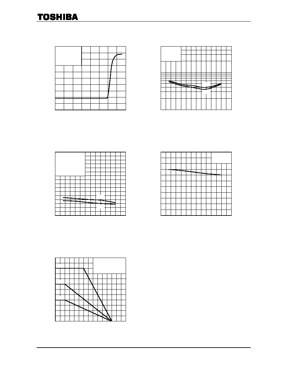
Output power POUT (W)
THD ≠ Pout
T
o
t
a
l
ha
rm
oni
c
dist
or
ti
on
T
H
D
(%
)
Output power POUT (W)
THD ≠ Pout
T
o
t
a
l
ha
rm
oni
c
dist
or
ti
on
T
H
D
(%
)
Frequency f (Hz)
THD ≠ f
T
o
t
a
l
ha
rm
oni
c
dist
or
ti
on
T
H
D
(%
)
Frequency f (Hz)
G
V
≠ f
Frequency f (Hz)
R.R. ≠ f
Signal source resistance Rg ()
R.R. ≠ Rg
R
i
pple
rej
e
ct
i
on
rati
o
R
.
R
.
(
d
B)
Rg
= 620
RL = 8
Vripple
= 0.775Vrms
VCC = 37 V
-70
-80
-30
-20
30 300
30k
100k
1k
3k
-60
-50
-40
-10
0
100
10k
OUT1
OUT2
fripple = 100 Hz
RL = 8
Vripple = 0.775Vrms
VCC = 37 V
-70
-80
-30
30
0.3
30 100k
1k
3k
-60
-50
-40
100
10k
OUT1
OUT2
0.1
0.03
0.5
1
0.3
100
RL = 8
f
= 1 kHz
Filter: 400~30 k
1 3
30
100
0.5
5 10
50
0.05
0.1
0.3
10
5
3
50
30
VCC = 15 V
37 42
0.03
0.01
0.5
1
30 300
30k
100k
1k
3k
0.05
0.1
0.3
5
10
100 10k
RL = 8
Pout
= 1 W
VCC = 37 V
Filter
~30 k (f
= 20~800)
400~30 k (f
= 1 k~2 k)
400~80 k (f
= 4 k~6 k)
400~ (f
= 8 k~40 k)
3
OUT2
OUT1
RL = 8
Vout = 0.775 Vrms
VCC = 37 V
20
15
40
45
30
300
30k 100k
1k
3k
25
30
35
100
10k
20
0.1
0.03
0.5
1
0.3
100
VCC = 37 V
RL = 8
Filter 100: ~30 k
1 k: 400~30 k
10 k: 400~
1 3
30
100
f
= 10 kHz
0.5 5
10
50
0.05
0.1
0.3
10
100 Hz
1 kHz
5
3
50
30

TA8258HQ
2004-04-06
9
Rg
= 620 k
RL = 8
VCC = 37 V
-70
-80
-30
-20
30 300
30k
100k
1k
3k
-60
-50
-40
-10
0
100
10k
OUT2
OUT1
OUT1
OUT2
Qui
e
s
c
en
t cu
r
r
ent
I CC
Q
(
m
A
)
Outp
ut
po
wer
P
ou
t
(W
)
Frequency f (Hz)
C.T. ≠ f
Cr
o
s
s
t
a
lk
C
.
T
.
(
d
B
)
Signal source resistance Rg ()
C.T. ≠ Rg
Cr
o
s
s
t
a
lk
C
.
T
.
(
d
B
)
Signal source resistance Rg ()
V
no
≠ Rg
O
u
tp
ut nois
e
v
o
lt
a
ge
V
NO
(
m
V
rm
s)
Supply voltage VCC (V)
P
out
≠ V
CC
Outp
ut D
C
v
o
l
t
a
ge
V
OU
T
(
V
)
Supply voltage VCC (V)
I
CCQ
, V
OUT
≠ V
CC
Output power Pout (W)
P
D
≠ P
OUT
Po
wer
dis
s
i
p
ati
on P
D
(
W
)
5
0
20
10
10
15
25
35
5 10
15
20
25 30 35 40
f
= 1 kHz
RL = 8
THD
= 10 %
45
30
RL = 8
VCC = 37 V
B.W = 20Hz~20kHz
100
0
500
600
30 300
30k
100k
1k
3k
200
300
400
700
800
100
10k
OUT2
OUT1
-70
-80
-30
30
300
30k 100k
1k
3k
-60
-50
-40
100
10k
f
= 1 kHz
RL = 8
VCC = 37 V
Vout = 0.775Vrms
OUT2
OUT1
OUT1
OUT2
f
= 1 kHz
RL = 8
5
0
0
10
15
5 10
25
20
15
20
37 V
25
15 V
42 V
0
0
40
60
100
120
10
20 40
30
RL = 8
VCC = 37 V
Vin = 0
50 60
20
80
0
20
60
40
ICCQ
VOUT
TA8258HQ
2004-04-06
10
0
0
10
25
25
50 100
175
75
1
5
15
20
30
125 150
1: INFINITE HEAT SINK
2: 4.1∞C/W A HEAT SINK
3: 9.5∞C/W A HEAT SINK
2
3
Mute control voltage Vmute (V)
ATT ≠ V
mute
Mut
e
A
T
T
(
d
B
)
Ambient temperature Ta (∞C)
P
D
MAX ≠ Ta
A
l
lo
wab
l
e p
o
w
e
r
di
s
s
ipati
o
n
P
D
M
A
X
(w)
f
= 1 kHz
RL = 8
Vout = 0.775Vrms
VCC = 37 V
-60
-80
8
-40
-20
1 2
4
3
0
10
Ambient temperature Ta (∞C)
THD ≠ Ta
T
o
t
a
l
ha
rm
oni
c
dist
or
tio
n
T
H
D
(%
)
RL = 8
VCC = 37 V
f
= 1 kHz
Pout
= 2 W
0.03
0.01
-40
0.05
0.1
0.2
-20
0 60
40
20
80 100
OUT1
OUT2
Ambient temperature Ta (∞C)
R.R. ≠ Ta
R
i
pple
rej
e
ct
i
on
rati
o
R
.
R
.
(
d
B)
Rg = 620
RL = 8
Vripple
= 0.775 Vrms
VCC = 37 V
fripple
= 100 Hz
-80
-40
-40
-20
-20 0
60
40
20
80 100
OUT1
OUT2
-70
-60
-50
-30
-10
0
Ambient temperature Ta (∞C)
I
CCQ
≠ Ta
Qui
e
s
c
en
t cu
r
r
ent
I CC
Q
(
m
A
)
VCC = 37 V
RL = 8
20
0
-40
40
60
80
-20
0 60
40
20
80 100
100

TA8258HQ
2004-04-06
11
Package Dimensions
Weight: 4.04 g (typ.)

TA8258HQ
2004-04-06
12
∑ The information contained herein is subject to change without notice.
∑ The information contained herein is presented only as a guide for the applications of our products. No
responsibility is assumed by TOSHIBA for any infringements of patents or other rights of the third parties which
may result from its use. No license is granted by implication or otherwise under any patent or patent rights of
TOSHIBA or others.
∑ TOSHIBA is continually working to improve the quality and reliability of its products. Nevertheless, semiconductor
devices in general can malfunction or fail due to their inherent electrical sensitivity and vulnerability to physical
stress. It is the responsibility of the buyer, when utilizing TOSHIBA products, to comply with the standards of
safety in making a safe design for the entire system, and to avoid situations in which a malfunction or failure of
such TOSHIBA products could cause loss of human life, bodily injury or damage to property.
In developing your designs, please ensure that TOSHIBA products are used within specified operating ranges as
set forth in the most recent TOSHIBA products specifications. Also, please keep in mind the precautions and
conditions set forth in the "Handling Guide for Semiconductor Devices," or "TOSHIBA Semiconductor Reliability
Handbook" etc..
∑ The TOSHIBA products listed in this document are intended for usage in general electronics applications
(computer, personal equipment, office equipment, measuring equipment, industrial robotics, domestic appliances,
etc.). These TOSHIBA products are neither intended nor warranted for usage in equipment that requires
extraordinarily high quality and/or reliability or a malfunction or failure of which may cause loss of human life or
bodily injury ("Unintended Usage"). Unintended Usage include atomic energy control instruments, airplane or
spaceship instruments, transportation instruments, traffic signal instruments, combustion control instruments,
medical instruments, all types of safety devices, etc.. Unintended Usage of TOSHIBA products listed in this
document shall be made at the customer's own risk.
∑ The products described in this document are subject to the foreign exchange and foreign trade laws.
∑ TOSHIBA products should not be embedded to the downstream products which are prohibited to be produced
and sold, under any law and regulations.
∑ This product generates heat during normal operation. However, substandard performance or malfunction may
cause the product and its peripherals to reach abnormally high temperatures.
The product is often the final stage (the external output stage) of a circuit. Substandard performance or
malfunction of the destination device to which the circuit supplies output may cause damage to the circuit or to the
product.
030619EBF
RESTRICTIONS ON PRODUCT USE