 | –≠–ª–µ–∫—Ç—Ä–æ–Ω–Ω—ã–π –∫–æ–º–ø–æ–Ω–µ–Ω—Ç: TA8259H | –°–∫–∞—á–∞—Ç—å:  PDF PDF  ZIP ZIP |
TA8259H
2002-03-05
1
TOSHIBA Bipolar Linear Integrated Circuit Silicon Monolithic
TA8259H
Max Power 37 W BTL ◊ 4CH Audio Power IC
The TA8259H is 4 ch BTL audio power amplifier for car audio
application.
This IC can generate more high power: P
OUT
MAX = 37 W as it is
included the pure complementary PNP and NPN transistor
output stage.
It is designed low distortion ratio for 4 ch BTL audio power
amplifier, built-in Stand-by Function, Muting Function, Clip
detector, and diagnosis circuit.
Additionally, the AUX. amplifier is built-in, it can make the beep
signal etc. output to 2 channels (OUT1 and 4).
It contains various kind of protectors for car audio use.
Features
∑ High power
:
P
OUT
MAX (1) = 37 W (typ.)
(V
CC
= 14.4 V, JEITA max, R
L
= 4 )
:
P
OUT
MAX (2) = 35 W (typ.)
(V
CC
= 13.7 V, JEITA max, R
L
= 4 )
:
P
OUT
(1) = 24 W (typ.)
(V
CC
= 14.4 V, f = 1 kHz, THD = 10%, R
L
= 4 )
:
P
OUT
(2) = 21 W (typ.)
(V
CC
= 13.2 V, f = 1 kHz, THD = 10%, R
L
= 4 )
∑ Built-in clip detector & diagnosis circuit. (pin 25)
∑ Low distortion ratio
: THD = 0.02% (typ.)
(V
CC
= 13.2 V, f = 1 kHz, P
OUT
= 5 W, R
L
= 4 )
∑ Low noise
:
V
NO
= 0.16 mVrms (typ.)
(V
CC
= 13.2 V, R
g
= 0 , G
V
= 34dB, BW = 20 Hz~20 kHz)
∑ Built-in stand-by switch function (pin 2)
∑ Built-in muting function (pin 24)
∑ Built-in AUX. amplifier from single input (pin 16) to 2 channels output ; OUT1 and 4
∑ Built-in various protection circuit
: Thermal shut down, over voltage, out to GND, out to V
CC
, out to out short
∑ Operating supply voltage: V
CC (opr)
= 9~18 V
Weight: 9.8 g (typ.)

TA8259H
2002-03-05
2
Block Diagram

TA8259H
2002-03-05
3
Caution and Application Method
(description is made only on the single channel)
1. Voltage gain adjustment
This IC has no NF (negative feedback) terminals. Therefore, the voltage gain can't adjusted, but it makes
the device a space and total costs saver.
Figure 1 Block diagram
The voltage gain of Amp. 1
: G
V1
= 8dB
The voltage gain of Amp. 2A, B
: G
V2
= 20dB
The voltage gain of BLT Connection : G
V (BTL)
= 6dB
Therefore, the total voltage gain is decided by expression below.
G
V
= G
V1
+ G
V2
+ G
V (BTL)
= 8 + 20 + 6 = 34dB
TA8259H
2002-03-05
4
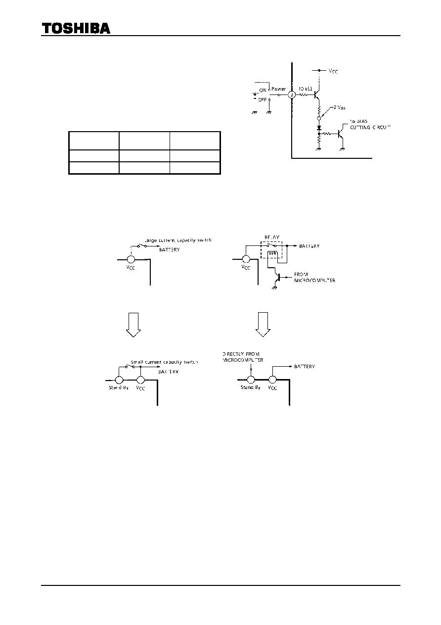
2. Stand-by SW function
(pin 2)
By means of controlling pin 2 (Stand-by terminal) to
High and Low, the power supply can be set to ON and
OFF.
The threshold voltage of pin 2 is set at about 3 V
BE
(typ.), and the Power Supply current is about 2 µA
(typ.) at the stand-by state.
Control voltage of pin 2: V
(SB)
Stand-By Power V
(SB)
(V)
ON OFF 0~1.5
OFF ON
3~
V
CC
Adjustage of stand-by SW
(1) Since
V
CC
can directly be controlled to ON or OFF by the microcomputer, the switching relay can be
omitted.
(2) Since the control current is microscopic, the switching relay of small current capacity is satisfactory
for switching
Conventional method
Stand-by switch method
Figure 3
Figure 2 With pin 2 set to high, power
is turned ON

TA8259H
2002-03-05
5
3. Muting
function
(pin 24)
By means of controlling pin 24 less than 0.5 V, it can make the audio muting condition.
The muting time constant is decided by R
1
and C
4
and these parts is related the pop noise at power
ON/OFF.The series resistance; R
1
must be set up less than 15 k, we recommend 10 k.
The muting function have to be controlled by a transistor, FET and µ-COM port which has I
MUTE
250 µA
ability.
Terminal 24 must not be pulled up and it shall be controlled by OPEN/LOW.
Figure 4 Muting function
Figure 5 Mute attenuation-V
mute
(V)
4. AUX.
input
(pin 16)
The pin 16 is for input terminal of AUX. amplifier.
The total gain is 0dB by using of AUX. amplifier.
Therefore, the µ-COM can directly drive the AUX. amplifier.
BEEP sound or voice synthesizer signal can be input to pin 16 directly.
Figure 6 AUX input