 | –≠–ª–µ–∫—Ç—Ä–æ–Ω–Ω—ã–π –∫–æ–º–ø–æ–Ω–µ–Ω—Ç: TA8275H | –°–∫–∞—á–∞—Ç—å:  PDF PDF  ZIP ZIP |
TA8275H
2002-02-13
1
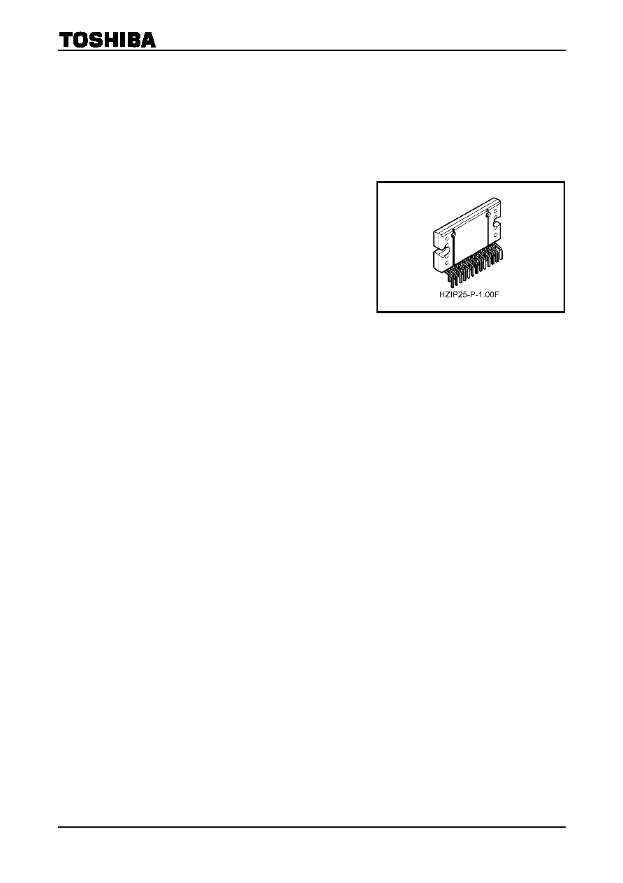
TOSHIBA Bipolar Linear Integrated Circuit Silicon Monolithic
TA8275H
Max Power 41 W BTL
¥
4 ch Audio Power IC
The TA8275H is 4 ch BTL audio power amplifier for car audio
application.
This IC can generate more high power: P
OUT
MAX = 41 W as it
is included the pure complementary PNP and NPN transistor
output stage.
It is designed low distortion ratio for 4 ch BTL audio power
amplifier, built-in stand-by function, muting function, output
clipping detection and diagnosis circuit which can detect output
to V
CC
/GND short and over voltage input mode.
Additionally, the AUX amplifier and various kind of protector
for car audio use are built-in.
Features
∑ High power : P
OUT
MAX (1) = 41 W (typ.)
(V
CC
= 14.4 V, f = 1 kHz, JEITA max, R
L
= 4 )
:
P
OUT
MAX (2) = 37 W (typ.)
(V
CC
= 13.7 V, f = 1 kHz, JEITA max, R
L
= 4 )
:
P
OUT
(1) = 24 W (typ.)
(V
CC
= 14.4 V, f = 1 kHz, THD = 10%, R
L
= 4 )
:
P
OUT
(2) = 21 W (typ.)
(V
CC
= 13.2 V, f = 1 kHz, THD = 10%, R
L
= 4 )
∑ Built-in output clipping detection and diagnosis circuit (pin 25)
∑ Low distortion ratio: THD = 0.02% (typ.)
(V
CC
= 13.2 V, f = 1 kHz, P
OUT
= 5 W, R
L
= 4 )
∑ Low noise: V
NO
= 0.10 mVrms (typ.)
(V
CC
= 13.2 V, R
g
= 0 , G
V
= 26 dB, BW = 20 Hz~20 kHz)
∑ Built-in stand-by switch (pin 4)
∑ Built-in muting function (pin 22)
∑ Built-in AUX amplifier from single input to 2 channels output (pin 16)
∑ Built-in various protection circuit
: Thermal shut down, over voltage, out to GND, out to V
CC
, out to out short, speaker burned
∑ Operating supply voltage: V
CC (opr)
= 9~18 V
Weight: 7.7 g (typ.)
TA8275H
2002-02-13
2
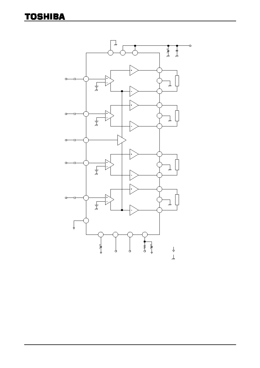
Block Diagram
R
L
R
L
R
L
11
9
8
7
5
2
3
17
18
19
21
24
23
12
15
14
1
20
6
R
L
IN1
IN2
IN3
AUX IN
IN4
13
16
C
1
C
1
C
1
C
1
PRE-GND
10
25
4
22
OUT1 (
+
)
PW-GND1
OUT1 (
-
)
OUT2 (
+
)
PW-GND2
OUT2 (
-
)
OUT3 (
+
)
PW-GND3
OUT3 (
-
)
OUT4 (
+
)
PW-GND4
OUT4 (
-
)
TAB
V
CC1
V
CC2
C
3
R
1
C
4
C
2
: PRE-GND
: PW-GND
STBY
CLIP OUT
&
DIAGNOSIS
OUT
RIP MUTE
C
5
C
6

TA8275H
2002-02-13
3
Figure 2 With pin 4 set to High,
Power is turned ON
ON
4
OFF
10 k
W
to BIAS
CUTTING CIRCUIT
ª
2V
BE
V
CC
Power
Caution and Application Method
(Description is made only on the single channel.)
1. Voltage
Gain
Adjustment
This IC has no NF (negative feedback) terminals. Therefore, the voltage gain can't adjusted, but it makes
the device a space and total costs saver.
The voltage gain of Amp.1:
G
V1
= 0 dB
The voltage gain of Amp.2A, B:
G
V2
= 20 dB
The voltage gain of BLT Connection: G
V (BTL)
= 6 dB
Therefore, the total voltage gain is decided by expression below.
G
V
= G
V1
+ G
V2
+ G
V (BTL)
= 0 + 20 + 6 = 26 dB
2. Stand-by SW Function
(pin 4)
By means of controlling pin 4 (stand-by terminal)
to high and low, the power supply can be set to ON
and OFF. The threshold voltage of pin 4 is set at
about 3V
BE
(typ.), and the power supply current is
about 2 mA (typ.) at the stand-by state.
Control Voltage of pin 4: V
SB
Stand-by Power V
SB
(V)
ON OFF 0~1.5
OFF ON 3~V
CC
Adjustage of Stand-by SW
(1) Since
V
CC
can directly be controlled to ON or OFF by the microcomputer, the switching relay can be
omitted.
(2) Since the control current is microscopic, the switching relay of small current capacity is satisfactory
for switching
Amp. 1
Input
Amp. 2A
Amp. 2B
Figure 1 Block Diagram

TA8275H
2002-02-13
4
3. Muting
Function
(pin 22)
By means of controlling pin 22 less than 0.5 V, it can make the audio muting condition.
The muting time constant is decided by R
1
and C
4
and these parts is related the pop noise at power
ON/OFF.
The series resistance; R1 must be set up less than 10 kW to get enough muting attenuation.
The muting function have to be controlled by a transistor, FET and m-COM port which has I
MUTE
> 250 mA
ability.
Pin 22 terminal voltage has the temperature characteristics of 4.6 V (low temperature) to 3.2 V (high
temperature).
Therefore, it is need to design with attention as using the microcontroller of which operating voltage is less
than 5 V.
Terminal 22 may not be pulled up and shall be controlled by OPEN/LOW.
When it is obliged to do, it must be pulled up via diode, because it has to defend flowing reverse current to
internal circuit of pin 22.
≠ Conventional Method ≠
V
CC
Large current capacity switch
BATTERY
V
CC
FROM
MICROCOMPUTER
BATTERY
RELAY
V
CC
Small current capacity switch
BATTERY
Stand-By
V
CC
DIRECTLY FROM
MICROCOMPUTER
BATTERY
Stand-By
≠ Stand-by Switch Method ≠
Figure 3
Figure 5 Mute Attenuation
-
-
-
-
V
MUTE
(V)
Point A voltage: VMUTE (V)
ATT ≠ V
MUTE
Mut
e
a
tte
nu
ati
o
n A
T
T
(dB
)
10 k
W
5 k
W
VCC
=
13.2 V
Po
=
10 W
PL
=
4
W
f
=
1 kHz
BW
=
400~30 kHz
-
100
0
0.4
0.8 1 1.2
1.6 2 2.4 2.8
3
-
80
-
60
-
40
-
20
0
20
Figure 4 Muting Function
R
1
I (100
m
A)
22
I
MUTE
I
MUTE (OFF)
A
V
MUTE
C
4
<Recommended Application>
<Application for pulled up>
R
1
I (100
m
A)
22
I
MUTE
I
MUTE (OFF)
V
MUTE
C
4

TA8275H
2002-02-13
5
4. AUX
Input
(pin 16)
The pin 16 is for input terminal of AUX
amplifier.
The total gain is 0 dB by using of AUX amplifier.
Therefore, the m-COM can directly drive the
AUX amplifier.
BEEP sound or voice synthesizer signal can be
input to pin 16 directly.
When AUX function is not used, this pin must be
connected to PRE-GND (pin 13) via a capacitor.
5.
Diagnosis Output
(pin 25)
This diagnosis output terminal of pin 25 has open collector output structure on chip as shown in Figure 7.
In case diagnosis circuit that detect unusual case is operated, NPN Tr. (Q1) is turned on.
It is possible to protect all the system of apparatus as well as power IC protection.
In case of being unused this function, use this IC as open-connection on pin 25.
5.1
In Case of Shorting Output to V
CC
/GND or Over Voltage Power Supplied
NPN Tr. (Q1) is turned on.
Threshold of over voltage protection: V
CC
= 22 V (typ.)
5.2
In Case of Shorting Output to Output
NPN Tr. (Q1) is turned on and off in response to the input signal voltage.
25
5 V
LED/LCD
ALAME
REGULATOR
OFF
(Flashing)
(Announcement from a speaker.)
(Relay
OFF)
m
-COM
MEMORY (Count and record)
Figure 8 Application 1
Figure 6 AUX Input
20 dB AMP.
IN
OUT (
+
)
OUT (
-
)
16
AUX-IN
-
20 dB
AUX AMP
m
-COM
Figure 7 Self Diagnosis Output
pin 25: Open collector output (active low)
Q1 is turned on
GND
5 V
t
V25
OUTPUT SHORT
PROTECTOR
OVER VOLTAGE
PROTECTOR
25
Q1
5 V