 | –≠–ª–µ–∫—Ç—Ä–æ–Ω–Ω—ã–π –∫–æ–º–ø–æ–Ω–µ–Ω—Ç: TA8409SG | –°–∫–∞—á–∞—Ç—å:  PDF PDF  ZIP ZIP |

TA8409S/SG, F/FG
2003-08-12
1
TOSHIBA Bipolar Linear Integrated Circuit Silicon Monolithic
TA8409S/SG, TA8409F/FG
Bridge Driver
The TA8409S/SG and TA8409F/FG are bridge drivers with
output voltage control.
Features
Modes available (CW/CCW/STOP/BRAKE)
Output current up to 0.4 A (AVE) and 1.0 A (PEAK)
Wide range of operating voltages
V
CC
(opr.) = 4.5 to 20 V
V
S
(opr.) = 0 to 20 V
V
ref
(opr.) = 0 to 20 V (V
ref
V
S
)
Built-in thermal shutdown
Standby mode available (STOP MODE)
Hysteresis for all inputs.
TA8409S/SG
TA8409F/FG
Weight
SIP9-P-2.54A: 0.92 g (typ.)
SSOP10-P-225-1.00: 0.09 g (typ.)
TA8409FG/SG:
The TA8409FG/SG is a Pb-free product.
The following conditions apply to solderability:
*Solderability
1. Use of Sn-63Pb solder bath
*solder bath temperature = 230∞C
*dipping time = 5 seconds
*number of times = once
*use of R-type flux
2. Use of Sn-3.0 Ag-0.5 Cu solder bath
*solder bath temperature = 245∞C
*dipping time = 5 seconds
*the number of times = once
*use of R-type flux

TA8409S/SG, F/FG
2003-08-12
2
Block Diagram
TA8409S/SG, TA8409F/FG
TA8409S/SG PIN : Non-connection
TA8409F/FG PIN, : Non-connection

TA8409S/SG, F/FG
2003-08-12
3
Pin Function
TA8409S/SG
Pin No.
Symbol
Functional Description
1 IN2
Input
terminal
2 V
CC
Supply voltage terminal for logic
3 OUT2
Output
terminal
4 NC
Non-connection
5 GND
GND
terminal
6 V
S
Supply voltage terminal for motor driver
7 OUT1
Output
terminal
8 V
ref
Reference voltage terminal for control circuit
9 IN1
Input
terminal
TA8409F/FG
Pin No.
Symbol
Functional Description
1 IN2
Input
terminal
2 V
CC
Supply voltage terminal for logic
3 OUT2
Output
terminal
4 NC
Non-connection
5 GND
GND
terminal
6 NC
Non-connection
7 V
S
Supply voltage terminal for motor driver
8 OUT1
Output
terminal
9 V
ref
Reference voltage terminal for control circuit.
10 IN1
Input
terminal
Function
Input Output
Mode
IN 1
IN 2
OUT1
OUT2
MB
0 0
STOP
1 0 H L
CW/CCW
0 1 L H
CCW/CW
1 1 L L
BRAKE
: High
impedance
Note: Inputs are all high active type.
TA8409S/SG, F/FG
2003-08-12
4
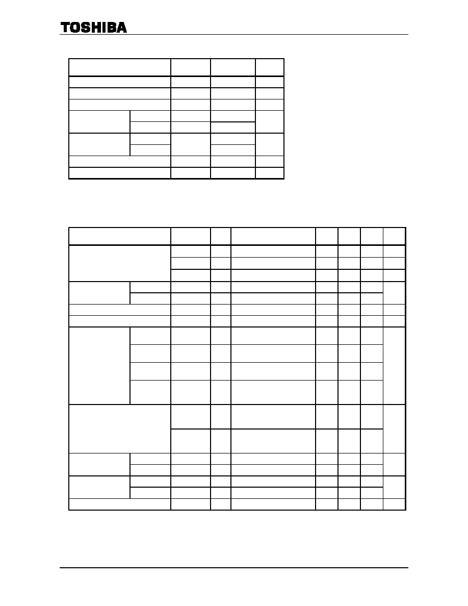
Maximum Ratings
(Ta = 25∞C)
Characteristics Symbol
Rating
Unit
Supply voltage
V
CC
25 V
Motor drive voltage
V
S
25 V
Reference voltage
V
ref
25 V
PEAK I
O
(PEAK)
1.0
Output current
AVE. I
O
(AVE.)
0.4
A
TA8409F/FG 0.735
(Note)
Power dissipation
TA8409S/SG
P
D
0.95
W
Operating temperature
T
opr
-30 to 75
∞C
Storage temperature
T
stg
-55 to 150
∞C
Note: This rating is obtained when the device is mounted on a 50 ◊ 50 ◊ 1.6 mm PCB with a Cu area of 30% or
more.
Electrical Characteristics
(Ta = 25∞C, V
CC
= 12 V, V
S
= 18 V)
Characteristics Symbol
Test
Circuit
Test Condition
Min
Typ.
Max
Unit
I
CC1
1
Output OFF, CW/CCW mode
10.0 15.0 mA
I
CC2
1
Output OFF, STOP mode
0 50 µA
Supply current
I
CC3
1
Output OFF, BREAK mode
6.5 10.0 mA
1 (High)
V
IN
1
2 T
j
= 25∞C IN1, 2
3.5
5.5
Input operating
voltage
2 (Low)
V
IN
2
2 T
j
= 25∞C IN1, 2
GND
0.8
V
Input current
I
IN
2 Sink
mode,
V
IN
= 3.5 V
3 10 µA
Input hysteresis voltage
V
T
2
0.7 V
Upper side
V
SAT
U-1
3
V
ref
= V
S
, V
OUT
-V
S
measure
I
O
= 0.2 A, CW/CCW mode
0.9 1.2
Lower side
V
SAT
L-1
3
V
ref
= V
S
, V
OUT
-GND measure
I
O
= 0.2 A, CW/CCW mode
0.8 1.2
Upper side
V
SAT
U-2
3
V
ref
= V
S
, V
OUT
-V
S
measure
I
O
= 0.4 A, CW/CCW mode
1.0 1.35
Saturation voltage
Lower side
V
SAT
L-2
3
V
ref
= V
S
, V
OUT
-GND
measure
I
O
= 0.4 A, CW/CCW mode
0.9 1.35
V
V
SAT
U-1'
3
V
ref
= 10 V, V
OUT
-GND
measure
I
O
= 0.2 A
10.4 11.2 12.2
Output voltage
V
SAT
U-2'
3
V
ref
= 10 V, V
OUT
-GND
measure
I
O
= 0.4 A
10.9
V
Upper side
I
LU
4 V
L
= 25 V
50
Output transistor
leakage current
Lower side
I
LL
4 V
L
= 25 V
50
µA
Upper side
V
F
U-1
5 I
F
= 0.4 A
1.5
Diode forward voltage
Lower side
V
F
L-1
5 I
F
= 0.4 A
0.9
V
Reference current
I
ref
2 V
ref
= 10 V, source mode
20 40 µA

TA8409S/SG, F/FG
2003-08-12
5
Test Circuit 1
I
CC1
,
I
CC2
,
I
CC3
Test Circuit 2
V
IN1
, V
IN2
, I
IN
,
V
T
, I
ref
TA8409S/SG, F/FG
TA8409S/SG, F/FG
TA8409S/SG, TA8409F/FG

TA8409S/SG, F/FG
2003-08-12
6
Test Circuit 3
V
SAT U-1, 2
,
V
SAT L-1, 2
,
V
SAT U-1', 2'
Note: Calibrate
I
OUT
to 0.2
/
0.4 A by R
L
.
Test Circuit 4
I
L U, L
Test Circuit 5
V
F U-1, 2
,
V
F L-1, 2
TA8409S/SG, F/FG
TA8409S/SG, F/FG
TA8409S/SG, F/FG
TA8409S/SG, TA8409F/FG
TA8409S/SG, TA8409F/FG

TA8409S/SG, F/FG
2003-08-12
7
TA8409F/FG
TA8409F/FG
TA8409S/SG,
TA8409S/SG,
TA8409S/SG
TA8409S/SG

TA8409S/SG, F/FG
2003-08-12
8
Application Circuit
Note 1: Attach a bypass capacitor to the Vs pin as required.
Note 2: Utmost care is necessary in the design of the output line, V
S
, V
CC
and GND line since the IC may be
destroyed by short-circuits between outputs, by supply faults, or by ground faults. Bear in mind also that
mounting the IC in the reverse orientation may also cause a breakdown.
Note 3: Switching the inputs may allow a pass-through current to flow. Keep the IC device in STOP mode (for at
least 100
µs) during the switching. Alternatively, insert a current-limiting resistor R.
Note 4: Use a current-limiting resistor R or fuse for overcurrent protection.
Note 5: When turning on the power for the IC device, apply VS after V
CC
(or V
CC
and V
S
simultaneously).
When shutting off the power, drop V
S
before V
CC
(or Vs and V
CC
simultaneously).
When turning on the power (V
CC
), keep both inputs (IN1 and IN2) on a low level.
TA8409S/SG, TA8409F/FG
7/8
GND
IN2
TA8409S/SG,F/FG
V
CC
V
S
IN1
R
M
10
µ
F
3/3
8/9
6/7
5/5
2/2
9/10
1/1
V
CC
V
S
V
ref
(Note)
OUT1
OUT2

TA8409S/SG, F/FG
2003-08-12
9
Package Dimensions
Weight: 0.92 g (typ.)

TA8409S/SG, F/FG
2003-08-12
10
Package Dimensions
Weight: 0.09 g (typ.)

TA8409S/SG, F/FG
2003-08-12
11
Notes on Contents
1. Block Diagrams
Some of the functional blocks, circuits, or constants in the block diagrams may be omitted or simplified for
explanatory purposes
.
2. Equivalent Circuits
The equivalent circuit diagrams may be simplified or some parts of them may be omitted for purposes.
3. Timing Charts
Timing charts may be simplified for explanatory purposes
.
4. Maximum Ratings
The absolute maximum ratings of a semiconductor device are a set of specified parameter values which must
not be exceeded during operation, even for an instant.
If any of these ratings are exceeded during operation, the device electrical characteristics may be irreparably
altered and the reliability and lifetime of the device can no longer be guaranteed.
Moreover, these operations with exceeded ratings may cause breakdown, damage and/or degradation to other
equipment. Applications using the device should be designed so that each maximum rating will never be
exceeded in any operating conditions.
Before using, creating and/or producing designs, refer to and comply with the precautions and conditions set
forth in this document.
5. Application Circuits
The application circuits shown in this document are provided for reference purposes only. Thorough
evaluation is required, especially at the mass production design stage.
Toshiba does not grant any license to any industrial property rights by providing these examples of application
circuits.
6. Test Circuits
Components in the test circuits are only used to obtain and confirm the device characteristics. These
components and circuits are not guaranteed to prevent malfunction or failure from occurring in the application
equipment.
About the handling of ICs
Install the product correctly to avoid breakdown, damage and/or degradation to the product or equipment.
About over-current protection and heat protection circuits
These protection functions are intended to guard against certain output short circuits or other abnormal
conditions with only temporary effect, and are not guaranteed to prevent the IC from being damaged.
These protection features may not be effective if the product is operated outside the guaranteed operating
ranges, and some output short circuits may result in the IC being damaged.
The overcurrent protection feature is only intended to protect the IC from a temporary short circuit.
Short circuits of longer duration may damage the IC through undue stress. The systems must be configured
so that any overcurrent condition will be eliminated as soon as possible.

TA8409S/SG, F/FG
2003-08-12
12
Counter-electromotive force
When the motor reverses or stops, counter-electromotive force in the motor may influence the current to flow
to the power source. If the power source lacks sink capability, the IC power and output pins may exceed the
rating. The counter-electromotive force of the motor varies depending on the conditions of use and the features
of the motor.
Therefore ensure that there is no damage to the IC or problem in operation, and no error in or damage to
peripheral circuits resulting from counter-electromotive force.
∑ The information contained herein is subject to change without notice.
∑ The information contained herein is presented only as a guide for the applications of our products. No
responsibility is assumed by TOSHIBA for any infringements of patents or other rights of the third parties which
may result from its use. No license is granted by implication or otherwise under any patent or patent rights of
TOSHIBA or others.
∑ TOSHIBA is continually working to improve the quality and reliability of its products. Nevertheless, semiconductor
devices in general can malfunction or fail due to their inherent electrical sensitivity and vulnerability to physical
stress. It is the responsibility of the buyer, when utilizing TOSHIBA products, to comply with the standards of
safety in making a safe design for the entire system, and to avoid situations in which a malfunction or failure of
such TOSHIBA products could cause loss of human life, bodily injury or damage to property.
In developing your designs, please ensure that TOSHIBA products are used within specified operating ranges as
set forth in the most recent TOSHIBA products specifications. Also, please keep in mind the precautions and
conditions set forth in the "Handling Guide for Semiconductor Devices," or "TOSHIBA Semiconductor Reliability
Handbook" etc..
∑ The TOSHIBA products listed in this document are intended for usage in general electronics applications
(computer, personal equipment, office equipment, measuring equipment, industrial robotics, domestic appliances,
etc.). These TOSHIBA products are neither intended nor warranted for usage in equipment that requires
extraordinarily high quality and/or reliability or a malfunction or failure of which may cause loss of human life or
bodily injury ("Unintended Usage"). Unintended Usage include atomic energy control instruments, airplane or
spaceship instruments, transportation instruments, traffic signal instruments, combustion control instruments,
medical instruments, all types of safety devices, etc.. Unintended Usage of TOSHIBA products listed in this
document shall be made at the customer's own risk.
∑ The products described in this document are subject to the foreign exchange and foreign trade laws.
∑ TOSHIBA products should not be embedded to the downstream products which are prohibited to be produced
and sold, under any law and regulations.
030619EBA
RESTRICTIONS ON PRODUCT USE