 | –≠–ª–µ–∫—Ç—Ä–æ–Ω–Ω—ã–π –∫–æ–º–ø–æ–Ω–µ–Ω—Ç: TA8696 | –°–∫–∞—á–∞—Ç—å:  PDF PDF  ZIP ZIP |

TA8696F
2002-02-13
1
TOSHIBA Bipolar Linear Integrated Circuit Silicon Monolithic
TA8696F
Correction IC for LCD TV
TA8696F operates with a power supply voltage of 3.3 to 7.5 V
and can be directly driven with a dry battery.
Features
∑ Enables high-precision correction using logarithmic
compression.
∑ correction for normally white LCD panel is possible.
∑ Offset/cancel input circuit enables high-quality correction
without distorting the primary color input signals.
∑ Cut-off voltage and drive voltage can be independently
controlled.
∑ Unsusceptible to negative effects of fluctuation of power
supply voltage.
∑ Either latch mode or through mode can be selected using the CH display mode switching pin.
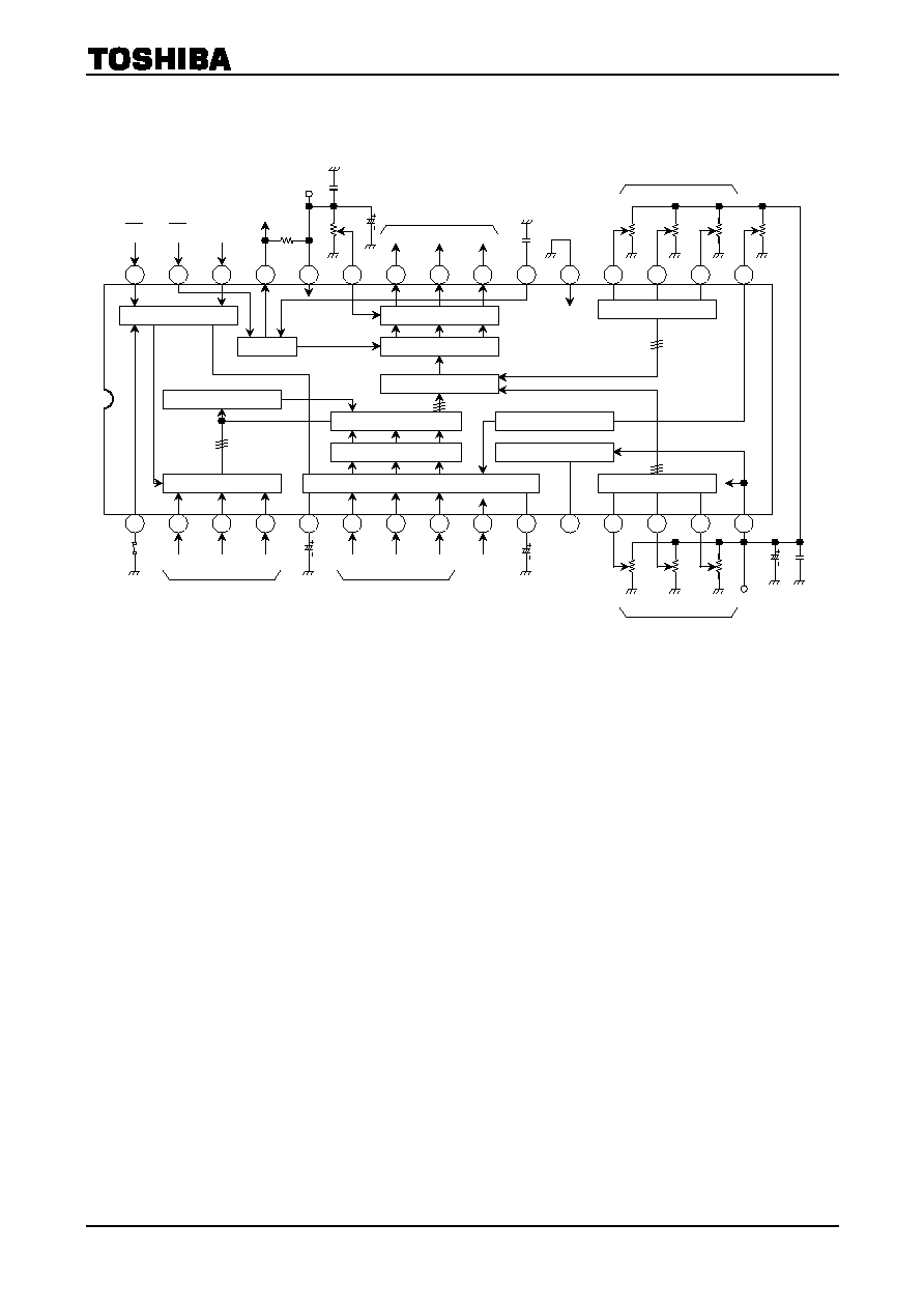
Block Diagram
Weight: 0.63 g (typ.)
HD
VD
B
CP
G
F.F. Output
R
BS/H
L.GND
F.F.
Control
H.GND
L.V
CC
(
+4 V)
RS/H
V
ref
Channel Mode
Offset, Cancel
Current Conversion
Pulse Modulation
Output Amp
Polarity Switching
Level Control
CH Display Switching
F.F.
g Correction
Input Latch
Input Detection
Current Conversion
Reference Voltage
Current Conversion
Channel Input
B G R
Input
B G
COM
Drive
B G
COM
B G R
Output
Cutoff
Input offset
control
V
O
Center
(
+13 V)
H.V
CC
30
1
29
2
28
3
27
4
26
5
25
6
24
7
23
8
22
9
21
10
20
11
19
12
18
13
17
14
16
15
TA8696F
2002-02-13
2
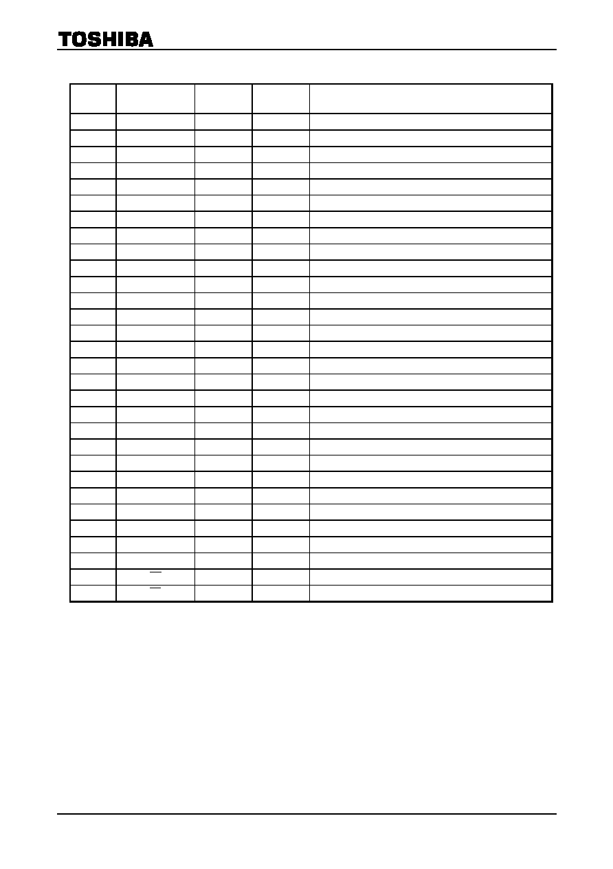
Pin Function
Pin No.
Pin Name
Reference
Voltage
(V)
Reference
Current
(mA)
Function
1
Mode Switch
0
0
CH display mode switching (latch mode/through mode)
2
CH B Input
0
0
CH display signal blue input
3
CH G Input
0
0
CH display signal green input
4
CH R Input
0
0
CH display signal red input
5
BS/H
1.6
0
Blue input signal sample and hold capacitor
6
B Input
1.6
0
Blue primary color input
7
G Input
1.6
0
Green primary color input
8
R Input
1.6
0
Red primary color input
9 L.GND 0
-8.1 Low-voltage
signal
GND
10
RS/H
1.6
0
Red input signal sample and hold capacitor
11 V
ref
1.6
0
Internal reference voltage
12
B Drive
2
0
B-axis drive control
13
R Drive
2
0
R-axis drive control
14
COM Drive
2
0
Common drive control
15 L.V
CC
4.0 8.1
Low-voltage
signal
V
CC
16
g Offset
2
0
g correction starting point control
17
COM Cut-off
2
0
Common cut-off control
18
R Cut-off
2
0
R-axis cut-off control
19 B
Cut-off 2
0
B-axis
cut-off
control
20 H.GND 0
-4.6 High-voltage
signal
GND
21 F.F.
CONT. 1.4
æ
æ
22
R Output
6.5
0
Red signal input
23
G Output
6.5
0
Green signal input
24
B Output
6.5
0
Blue signal input
25 V
O
Center
6.5
0
Signal output center voltage control
26 H.V
CC
13.0 4.6
High-voltage
signal
V
CC
27 F.F.
Output 0.2
0
Flip-flop
output
28
CP
0.9
0
Clamp pulse input
29
VD
1.4
0
Vertical drive pulse input
30
HD
0.9
0
Horizontal drive pulse input
Note 1: Reference voltage and reference current are for DC bias with no signal.
The current which flows into the IC considered to be positive current.

TA8696F
2002-02-13
3
Pin No.
Pin Name and Function
Typical Signal Level
Interface Current
1
Mode switch
Switches channel indication
mode
High level: Character mode
Low level: Latch mode
(synchronized with HD)
Internal bias
0 V
V
iH
= L.V
CC
V
iL
= GND
V
TH
= 1.9 V
V
iH Max
= L.V
CC
V
iL Min
= GND
Clamped on L.V
CC
and GND
2
3
4
CH B input
CH G input
CH R input
Channel indication signal
Input pin
Internal bias
0 V
V
iH Max
= 5.5 V
V
iL Min
= GND
Clamped on GND
5
10
BS/H
RS/H
Regenerate B/R-axis direct
current voltage
Capaciator pin
Internal bias
1.6 V
External capacitance 1
mF
Permissible load current
0
Clamped on L.V
CC
and GND
6
7
8
B input
G input
R input
Primary color input pins
Internal bias
1.6 V
White signal level
1.6 V
Black signal level
0.9 V
Maximum input level 1.4 V
p-p
Clamped on L.V
CC
and GND
11
V
ref
Internal standard voltage
reference pin
Internal bias
1.6 V
Permissible load current
0
Clamped on L.V
CC
and GND
5 V
0 V
V
TH
= 1.7 V
L.V
CC
30 k
W
50 k
W
1
40 k
W
60 k
W
2
3
4
100
W
1 k
W
5
10
100
W
1 k
W
L.V
CC
50
m
A
6
7
8
L.V
CC
50
m
A
14 k
W
50
m
A
8 k
W
2 k
W
11
L.V
CC
50
m
A
5 k
W
30 k
W
32 k
W

TA8696F
2002-02-13
4
Pin No.
Pin Name and Function
Typical Signal Level
Interface Current
12
13
18
19
B drive
R drive
R cut-off
B cut-off
Internal bias L.V
CC
/2
V
iH Max
= L.V
CC
V
iL Min
= GND
Clamped on L.V
CC
and GND
14
17
COM drive
COM cut-off
Internal bias L.V
CC
/2
V
iH Max
= L.V
CC
V
iL Min
= GND
Clamped on L.V
CC
and GND
16
g off-set
Internal bias L.V
CC
/2
V
iH Max
= L.V
CC
V
iL Min
= GND
Clamped on L.V
CC
and GND
22
23
24
R output
G output
B output
Inverted in sync with VD
Clamped on H.V
CC
and GND
L.V
CC
50
m
A
5 k
W
20 k
W
40 k
W
50
m
A
14
17
H.V
CC
50 k
W
22
23
24
100
m
A
50 k
W
25 k
W
6.
5 k
W
6.
5 k
W
11.5 Black
signal level
6.5
8.5 White
signal level
4.5 White
signal level
1.5 Black
signal level
12
13
18
19
L.V
CC
50
m
A
40 k
W
50
m
A
5 k
W
5 k
W
150
m
A
16
L.V
CC
50
m
A
40 k
W
5 k
W
100
m
A

TA8696F
2002-02-13
5
Pin No.
Pin Name and Function
Typical Signal Level
Interface Current
25 V
O
center
Internal bias H.V
CC
/2
V
iH Max
= H.V
CC
V
iL Min
= GND
Clamped on H.V
CC
and GND
27 F.F.
output
Desaturated open collector
output
Maximum sink current
0.5
mA
(V
oL Max
= 0.3 V)
V
oH Max
= H.V
CC
Clamped on H.V
CC
and GND
28
CP
Clamp pulse input
Be sure CP is correspondent
to the back porch of primary
color input signal.
V
TH
= 1.6 V
V
iH Max
= 5.5 V
V
iL Min
= GND
Clamped on H.V
CC
and GND
29
VD
input
Vertical drive pulse input
Be sure
VD
falls within the
vertical blanking period of
primary color input signal.
V
TH
=
V
iH Max
= 5.5 V
V
iL Min
= GND
Clamped on H.V
CC
and GND
30
HD
input
Be sure
HD
falls within the
horizontal blanking period of
primary color input signal.
V
TH
= 0.9 V
V
iH Max
= 5.5 V
V
iL Min
= GND
Clamped on GND
28
L.V
CC
1 k
W
50
m
A
29
H.V
CC
45 k
W
21
3.0 V
30
1 k
W
50
m
A
L.V
CC
50
m
A
Input
CP
5 V
0 V
5 V
0 V
1 V
5 V
0 V
1 H
25
H.V
CC
65 k
W
65 k
W
100
m
A
27
H.V
CC
13
W
30
W
8 k
W

TA8696F
2002-02-13
6
Maximum Ratings
(Ta
=
=
=
=
25∞C)
Characteristics Symbol
Rating
Unit
Power supply voltage
L.V
CC
8 V
Power supply voltage
H.V
CC
14.5 V
Power dissipation
P
D
890
mW
Power dissipation lowering rate
q
ja
7.2
mW/∞C
Operating temperature
T
opr
-20 to +75 ∞C
Storage temperature
T
stg
-55 to 150
∞C
Note 2: When the IC is operated at 25∞C or higher, reduce power dissipation by 12.8 mW per degree.
Recommended Power Supply Voltage
Pin
No.
Pin Name
Min
Typ.
Max
Unit
15 L.V
CC
3.3
5.0
7.5
26
H.V
CC
10.0
13.0
14.0
V
Electrical Characteristics
(unless otherwise specified, V
CC
=
=
=
=
4 V, Ta
=
=
=
=
25∞C)
Characteristics Symbol
Test
Circuit
Test Condition
Min
Typ.
Max
Unit
[1] Operating
range
Primary color input white signal level
æ 2
The same conditions are given
to R/G/B-axis.
æ 1.6 æ V
Primary color input black signal level
æ 2
The same conditions are given
to R/G/B-axis.
æ 0.9 æ V
CH indication signal level
æ 2
The same conditions are given
to R/G/B-axis.
3 5 5.5 V
Timing pulse level
æ 2
HD
,
VD
,
LD
3
5
5.5
V
[2] Electrical
characteristics
Operating power supply current (1)
æ 2
Pin
15.L.V
CC
= 4 V No load.
5.8
8.4
10.9
mA
Operating power supply current (2)
æ 2
Pin
26.H.V
CC
= 13 V No load.
3.2
4.6
6.0
mA
Input signal dynamic range
æ 2
æ
1.2 1.4 1.6 V
Input signal pin resistor
R
IN
2
æ
10.5 14.0 17.5
k
W
Input signal pin capacity
C
IN
2
æ
æ 1 3 pF
Black signal level off-set
æ 2
g off-set open
æ 100 200
mV
Black signal level off-set difference in
the axes
æ 2
æ
æ 50 100
mV
Black signal level off-set adjustment
amount
æ 2
æ
æ 0.3 æ V
Black signal level off-set adjustment
sensitivity
æ 2
æ
æ 300 æ mV/V
Input off-set elimination capacity
æ
2
æ 20
26
æ dB
Off-set cancel difference in the axes
æ
2
æ
æ 50 æ mV
Typical gain
æ
2
Drive adjustment open
9.4
12.4
15.4
dB
Typical gain difference in the axes
æ
2
Drive adjustment open
æ 0.5 æ dB
Typical gain difference in the polarity
æ
2
Drive adjustment open
æ 0.5 æ dB
Maximum gain
æ
2
æ 15.4
18.4
æ dB
Minimum gain
æ
2
æ
æ
-20
-10
dB

TA8696F
2002-02-13
7
Characteristics Symbol
Test
Circuit
Test Condition
Min
Typ.
Max
Unit
Gain control sensitivity
æ
2
æ
æ 6 æ dB/V
Polarity reverse center voltage
æ
2
V
o
center pin open
6.3
6.5
6.7
V
Polarity reverse center voltage
difference in the axes
æ
2
æ
æ 50 100
mV
Polarity reverse center voltage
variable range
æ
2
æ
æ 2 æ V
Polarity reverse center voltage
controlling sensitivity
æ
2
æ
æ 1 æ V/V
Typical cut-off level (N.W)
æ
2
Difference from V
o
center
voltage
±4.8
±5
±5.2
V
Cut-off level difference in the axes
æ
2
æ
æ 50 100
mV
Cut-off level variable amount
æ
2
æ
æ
±4
æ V
Cut-off level controlling sensitivity
æ
2
æ
æ 2 æ V/V
Output dynamic range
æ
2
æ
æ 10 æ
V
p-p
Output impedance
æ
2
æ
æ 10 æ
W
Frequency characteristic
æ
2
Loaded amount 120 pF,
-3dB
point
3 4
æ MHz
Frequency characteristic difference in
the axes
æ
2
Loaded amount 120 pF,
-3dB
point
æ 0.1 0.3 MHz
Slew rate
æ
2
Loaded amount 120 pF
æ 4 æ V/ms
Slew rate difference in the axes
æ
2
Loaded amount 120 pF
æ
æ 10 %
Crosstalk in the axes
æ
2
æ
æ 50 40 dB
Direct current transmission rate
æ
2
æ
æ 100 æ %
S/N N
æ
2
æ 40
50
æ dB
CH indication signal threshold
æ
2
æ
æ 2.2 æ V
CH indication mode switch threshold
æ
2
æ
æ 2.2 æ V
CH indication output delay (line mode)
æ
2
æ
æ 1 æ
ms
CH indication output delay (dot mode)
æ
2
æ
æ 0.1 æ
ms
CH indication latch minimum
operation voltage
æ
2
æ
æ
æ 3 V
HD pulse threshold
æ
2
æ
1.3 1.6 1.9 V
LD pulse threshold
æ
2
æ
1.3 1.6 1.9 V
VD pulse threshold
æ
2
æ
1.3 1.6 1.9 V
F.F. minimum operation voltage
æ
2
æ
æ
æ 10 V
F.F. phase delay
æ
2
æ
æ 3 æ
ms
F.F. response frequency
æ
2
æ 20
æ
æ kHz
F.F. output high level
æ
2
æ 11.0
13.0
æ V
F.F. output low level
æ
2
æ
0.1 0.3 0.5 V
g correction value (1) NW
æ
2
æ
æ 0.35 æ
æ
g correction value (2) NW
æ
2
æ
æ 20 æ
æ
g correction value difference in the
axes (1)
æ
2
æ
æ
æ 10 %
g correction value difference in the
axes (2)
æ
2
æ
æ
æ 10 %

TA8696F
2002-02-13
8
Test Circuit 1
Direct Current Characteristic
Note 3: Connect test pins directly to IC pins. (not shown above.)
Test value is written as V.1 to V.30.
Test Circuit 2
Alternating Current Characteristic
Note 4: The numbers of testing pins are not shown above because they are the same as IC pin numbers.
B G R
BS/H
L.GND
L.V
CC
RS/H
Channel Input
B G R
Input
B G
COM
Drive
HD
VD
CP F.F.
Output
H.GND
B G
COM
B G R
Output Cutoff
g Offset
V
O
Center
H.V
CC
Channel
Mode
V
ref
SW
13
T1 to T30
Power supply and bias signal apply pins.
C
10
1
m
F
/
50 V
C
5
1
m
F
/
50 V
V
R1
2
20 k
W
V
R1
3
20 k
W
V
R1
4
20 k
W
C
15A
10
m
F
/
10 V
C
15B
0.
01
m
F
T15
L.V
CC
SW
12
SW
14
SW
11
V
R1
6
20 k
W
V
R1
7
20 k
W
V
R1
8
20 k
W
V
R1
9
20 k
W
SW
18
SW
19
SW
17
SW
16
C
22
120 pF
C
23
120 pF
C
24
120 pF
V
R2
5
50 k
W
10
m
F
/
25 V
C
26B
0.
01
m
F
R
27
20 k
W
C
26A
SW
24
SW
25
SW
23
SW
22
T26 H.V
CC
M1 to M30
Power voltage and waveform testing pins.
30
1
29
2
28
3
27
4
26
5
25
6
24
7
23
8
22
9
21
10
20
11
19
12
18
13
17
14
16
15
B G R
BS/H
L.GND
L.V
CC
RS/H
Channel Input
B G R
Input
B G
COM
Drive
HD
VD
CP F.F.
Output
H.GND
B G
COM
B G R
Output Cutoff
g Offset
V
O
Center
H.V
CC
Channel
Mode
V
ref
C
10
1
m
F
/
50 V
C
5
1
m
F
/
50 V
10
m
F
/
10 V
C
15B
0.
01
m
F
L.V
CC
4.0 V
10
m
F
/
25 V
C
26B
0.
01
m
F
C
26A
H.V
CC
13.0 V
30
1
29
2
28
3
27
4
26
5
25
6
24
7
23
8
22
9
21
10
20
11
19
12
18
13
17
14
16
15
C
15A

TA8696F
2002-02-13
9
Input level (V)
g Curve (G-axis)
Outp
ut l
e
vel
(V
)
V
in
(V)
Input/Output Characteristic to V
14
V
out
(V
)
V
in
(V)
Input/Output Characteristic
to a Change of V
16
V
out
(V
)
V
in
(V)
Input/Output Characteristic to V
17
V
out
(V
)
V17 = 0.5 Æ 3.5 V
V17 = 0.5 V
V17 = 3.5 V
V17 = 2.0 V
13
0
1.3
2.6
3.9
5.2
6.5
7.8
9.1
10.4
11.7
0 0.2 0.4 0.6 0.8 1 1.2 1.4 1.6 1.8 2
V16 = 2.0 V
V16 = 3.0 V
V16 = 1.0 V
V16 = 4.0 V
11.5
1.5
2.5
3.5
4.5
5.5
6.5
7.5
8.5
9.5
10.5
0 0.2 0.4 0.6 0.8 1 1.2 1.4 1.6 1.8 2.0
5.0
1.0
1.0
Adjustment point
2.0
3.0
4.0
0.8
1.2 1.4 1.6
Drive adjustment point
11.5
1.5
0
V14 = 0.5 Æ 3.5 V
V14 = 0.5 V
V14 = 3.5 V
0.2 0.4 0.6 0.8 1 1.2 1.4 1.6 1.8 2
2.5
3.5
4.5
5.5
6.5
7.5
8.5
9.5
10.5
TA8696F
2002-02-13
10
Typical Application Circuits
All control VR is 20 kB. Connect 0.01 mF close to each control pin.
HD
VD
B
CP
G
F.F. Output
R
BS/H
L.GND
H.GND
L.V
CC
(
+4 V)
RS/H
Channel Mode
Offset, Cancel
Current Conversion
Pulse Modulation
Output Amp
Polarity Switching
Level Control
CH Display Switching
F.F.
g Correction
Input Latch
Input Detection
Current Conversion
Reference Voltage
Current Conversion
Channel Input
B G R
Input
B G
COM
Drive
B G
COM
B G R
Output
Cutoff
Input offset
control
V
O
Center
H.V
CC
(
+13 V)
30
1
29
2
28
3
27
4
26
5
25
6
24
7
23
8
22
9
21
10
20
11
19
12
18
13
17
14
16
15
47
m
F
20 k
W
0.
01
m
F
1
m
F
47
m
F
0.
01
m
F
1
m
F
0.
01
m
F
TA8696F
2002-02-13
11
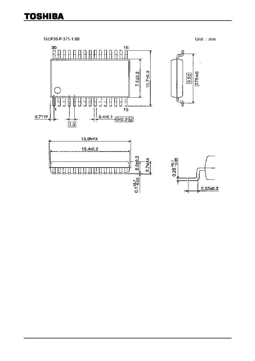
Package Dimensions
Weight: 0.63 g (typ.)

TA8696F
2002-02-13
12
∑ TOSHIBA is continually working to improve the quality and reliability of its products. Nevertheless, semiconductor
devices in general can malfunction or fail due to their inherent electrical sensitivity and vulnerability to physical
stress. It is the responsibility of the buyer, when utilizing TOSHIBA products, to comply with the standards of
safety in making a safe design for the entire system, and to avoid situations in which a malfunction or failure of
such TOSHIBA products could cause loss of human life, bodily injury or damage to property.
In developing your designs, please ensure that TOSHIBA products are used within specified operating ranges as
set forth in the most recent TOSHIBA products specifications. Also, please keep in mind the precautions and
conditions set forth in the "Handling Guide for Semiconductor Devices," or "TOSHIBA Semiconductor Reliability
Handbook" etc..
∑ The TOSHIBA products listed in this document are intended for usage in general electronics applications
(computer, personal equipment, office equipment, measuring equipment, industrial robotics, domestic appliances,
etc.). These TOSHIBA products are neither intended nor warranted for usage in equipment that requires
extraordinarily high quality and/or reliability or a malfunction or failure of which may cause loss of human life or
bodily injury ("Unintended Usage"). Unintended Usage include atomic energy control instruments, airplane or
spaceship instruments, transportation instruments, traffic signal instruments, combustion control instruments,
medical instruments, all types of safety devices, etc.. Unintended Usage of TOSHIBA products listed in this
document shall be made at the customer's own risk.
∑ The products described in this document are subject to the foreign exchange and foreign trade laws.
∑ The information contained herein is presented only as a guide for the applications of our products. No
responsibility is assumed by TOSHIBA CORPORATION for any infringements of intellectual property or other
rights of the third parties which may result from its use. No license is granted by implication or otherwise under
any intellectual property or other rights of TOSHIBA CORPORATION or others.
∑ The information contained herein is subject to change without notice.
000707EBA
RESTRICTIONS ON PRODUCT USE