 | –≠–ª–µ–∫—Ç—Ä–æ–Ω–Ω—ã–π –∫–æ–º–ø–æ–Ω–µ–Ω—Ç: TB1227CNG | –°–∫–∞—á–∞—Ç—å:  PDF PDF  ZIP ZIP |

TB1227CNG
2004-05-24
1
TOSHIBA Bi-CMOS INTEGRATED CIRCUIT
SILICON MONOLITHIC
TB1227CNG
VIDEO, CHROMA AND SYNCHRONIZING SIGNALS PROCESSING IC FOR PAL / NTSC
/ SECAM SYSTEM COLOR TV
TB1227CNG that is a signal processing IC for the PAL / NTSC /
SECAM color TV system integrates video, chroma and
synchronizing signal processing circuits together in a 56-pin
shrink DIP plastic package.
TB1227CNG incorporates a high performance picture quality
compensation circuit in the video section, an automatic PAL /
NTSC / SECAM discrimination circuit in the chroma section, and
an automatic 50 / 60Hz discrimination circuit in the
synchronizing section. Besides a crystal oscillator that internally
generates 4.43MHz, 3.58MHz and M / N-PAL clock signals for
color demodulation, there is a horizontal PLL circuit built in the
IC.
The PAL / SECAM demodulation circuit which is an adjustment-free circuit incorporates a 1H DL circuit inside for
operating the base band signal processing system.
Also, TB1227CNG makes it possible to set or control various functions through the built-in I
2
C bus line.
FEATURES
Video section
∑ Built-in trap filter
∑ Black expansion circuit
∑ Variable DC regeneration rate
∑ Y delay line
∑ Sharpness control by aperture control
∑ correction
∑ VSM output
Chroma section
∑ Built-in 1H Delay circuit
∑ PAL / SECAM base band demodulation system
∑ One crystal color demodulation circuit
(4.43MHz, 3.58MHz, M / N-PAL)
∑ Automatic system discrimination, system forced mode
∑ 1H delay line also serves as comb filter in NTSC demodulation
∑ Built-in band-pass filter, SECAM bell filter
∑ Color limiter circuit
∑ Fsc output
Synchronizing deflecting section
∑ Built-in horizontal VCO resonator
∑ Adjustment-free horizontal / vertical oscillation by count-down circuit
∑ Double AFC circuit
∑ Vertical frequency automatic discrimination circuit
∑ Horizontal / vertical holding adjustment
∑ Vertical ramp output
∑ Vertical amplitude adjustment
∑ Vertical linearity / S-shaped curve adjustment
Weight: 5.55 g (typ.)
TENTATIVE

TB1227CNG
2004-05-24
2
∑ SCP (Sand Castle Pulse) output
Text section
∑ Linear RGB input
∑ OSD RGB input
∑ Cut / off-drive adjustment
∑ RGB primary signal output

TB1227CNG
2004-05-24
3
BLOCK DIAGRAM

TB1227CNG
2004-05-24
4
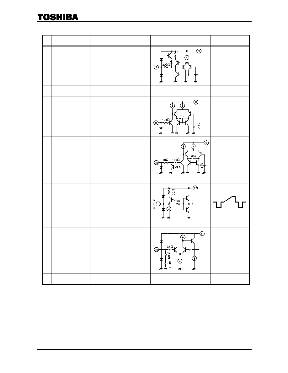
TERMINAL FUNCTIONS
PIN
No.
PIN NAME
FUNCTION
INTERFACE CIRCUIT
INPUT /
OUTPUTSIGNAL
1 SCP
OUTPUT
Output terminal of Sand Castle
Pulse. (SCP)
To connect drive resistor for SCP.
2 V-AGC
Controls pin 52 to maintain a
uniform V-ramp output.
Connect a current smoothing
capacitor to this pin.
--
3 H-V
CC
(9V)
V
CC
for the DEF block (deflecting
system).
Connect 9V (Typ.) to this pin.
-- --
4 Horizontal Output Horizontal output terminal.
5
Picture Distortion
Correction
Corrects picture distortion in high
voltage variation. Input AC
component of high voltage variation.
For inactivating the picture distortion
correction function, connect 0.01µF
capacitor between this pin and GND.
4.5V at Open
6 FBP
Input
FBP input for generating horizontal
AFC2 detection pulse and horizontal
blanking pulse.
The threshold of horizontal AFC2
detection is set H.V
CC
-2V
f
(V
f
0.75V).
Confirming the power supply
voltage, determine the high level of
FBP.
TB1227CNG
2004-05-24
5
PIN
No.
PIN NAME
FUNCTION
INTERFACE CIRCUIT
INPUT / OUTPUT
SIGNAL
7 Coincident
Det.
To connect filter for detecting
presence of H. synchronizing signal
or V. synchronizing signal.
--
8 V
DD
(5V)
V
DD
terminal of the LOGIC block.
Connect 5V (Typ.) to this pin.
-- --
9 SCL
SCL terminal of I
2
C bus.
--
10 SDA
SDA terminal of I
2
C bus.
11 Digital GND
Grounding terminal of LOGIC block.
--
--
12
13
14
B Output
G Output
R Output
R, G, B output terminals.
15 TEXT GND
Grounding terminal of TEXT block.
--
--
16 ABCL
External unicolor brightness control
terminal. Sensitivity and start point
of ABL can be set through the bus.
6.4V at Open
17 RGB-V
CC
(9V)
V
CC
terminal of TEXT block.
Connect 9V (Typ.) to this pin.
-- ----

TB1227CNG
2004-05-24
6
PIN
No.
PIN NAME
FUNCTION
INTERFACE CIRCUIT
INPUT / OUTPUT
SIGNAL
18
19
20
Digital R Input
Digital G Input
Digital B Input
Input terminals of digital R, G, B
signals. Input DC directly to these
pins.
OSD or TEXT signal can be input to
these pins.
OSD
3.0V
TEXT
2.0V
GND
21 Digital YS / YM
Selector switch of halftone / internal
RGB signal / digital RGB
(pins 18, 19, 20).
OSD
3.0V
TEXT
2.0V
H.T.
1.0V
TV
GND
22 Analog
YS
Selector switch of internal RGB
signal or analog RGB
(pins 23, 24, 25).
Analog RGB
0.5V
TV
GND
23
24
25
Analog R Input
Analog G Input
Analog B Input
Analog R, G, B input terminals. Input
signal through the clamping
capacitor. Standard input level :
0.5V
p-p
(100 IRE).
26 Color
Limiter
To connect filter for detecting color
limit.
--
27 FSC Output
Output terminal of FSC.

TB1227CNG
2004-05-24
7
PIN
No.
PIN NAME
FUNCTION
INTERFACE CIRCUIT
INPUT / OUTPUT
SIGNAL
28 1Bit DAC Output
Terminal
Enable to change slave address to
8Ah by a connecting V
CC
with this
terminal.
29 VSM
Output
Terminal
Power output the signal that is
primary differentiated Y signal.
Enable to change output amplifier
and phase by the Bus.
--
30 APC
Filter
To connect APC filter for chroma
demodulation.
DC
3.2V
31 Y
2
Input
Input terminal of processed Y signal.
Input Y signal through clamping
capacitor. Standard input level :
0.7V
p-p
32 Fsc
GND
Grounding terminal of VCXO block.
Insert a decoupling capacitor
between this pin and pin 38 (Fsc
V
DD
) at the shortest distance from
both.
-- --
33
34
B-Y Input
R-Y Input
Input terminal of B-Y or R-Y signal.
Input signal through a clamping
capacitor.
DC
2.5V
AC
B-Y : 650mV
p-p
R-Y : 510mV
p-p
(with input of PAL-75%
color bar signal)

TB1227CNG
2004-05-24
8
PIN
No.
PIN NAME
FUNCTION
INTERFACE CIRCUIT
INPUT / OUTPUT
SIGNAL
35
36
R-Y Output
B-Y Output
Output terminal of demodulated R-Y
or B-Y signal. There is an LPF for
removing carrier built in this pin.
DC
1.9V
AC
B-Y : 650mV
p-p
R-Y : 510mV
p-p
(with input of PAL-75%
color bar signal)
37 Y
Output
Output terminal of processed Y
signal. Standard output level :
0.7V
p-p
38 Fsc
V
DD
V
DD
terminal of DDS block. Insert a
decoupling capacitor between this
pin and pin 32 (Fsc GND) at the
shortest distance from both. If
decouping capacitor is inserted at a
distance from the pins, it may cause
spurious deterioration.
-- --
39 Black
Stretch
To connect filter for controlling black
expansion gain of the black
expansion circuit. Black expansion
gain is determined by voltage of this
pin.
DC
1.6V
40 16.2MHz
X'tal
To connect 16.2MHz crystal clock
for generating sub-carrier.
Lowest resonance frequency (f
0
) of
the crystal oscillation can be varied
by changing DC capacity. Adjust f
0
of the oscillation frequency with the
board pattern.
DC
4.1V

TB1227CNG
2004-05-24
9
PIN
No.
PIN NAME
FUNCTION
INTERFACE CIRCUIT
INPUT / OUTPUT
SIGNAL
41 Y / C V
CC
(5V)
V
CC
terminal of Y / C signal
processing block.
-- --
42 Chroma
Input
Chroma signal input terminal. Input
negative 1.0V
p-p
sync composite
video signal to this pin through a
coupling capacitor.
DC
2.4V
AC : 300mV
p-p
burst
43 Y / C GND
Grounding terminal of Y / C signal
processing block.
-- --
44 APL
To connect filter for DC regeneration
compensation.
Y signal after black expansion can
be monitored by opening this pin.
DC
2.2V
45 Y
1
Input
Input terminal of Y signal. Input
negative 1.0V
p-p
sync composite
video signal to this pin through a
clamping capacitor.
46 S-Demo-Adj.
To connect f
0
adjustment filter for
SECAM demodulation.
DC
3.2V
47 V-Center
DC Output Terminal For V Centering.
Enable to control output DC voltage
by the bus.
DC
2.7~6.3V

TB1227CNG
2004-05-24
10
PIN
No.
PIN NAME
FUNCTION
INTERFACE CIRCUIT
INPUT / OUTPUT
SIGNAL
48 AFC1
Filter
To connect filter for horizontal AFC1
detection.
Horizontal frequency is determined
by voltage of this pin.
DC
5.0V
49 Sync
Output
Output terminal of synchronizing
signal separated by sync separator
circuit.
Connect a pull-up resistor to this pin
because it is an open-collector
output type.
50 V-Sepa.
To connect filter for vertical
synchronizing separation.
DC
5.9V
51 Sync
Input
Input terminal of synchronizing
separator circuit. Input signal
through a clamping capacitor to this
pin. Negative 1.0V
p-p
sync.
52 V-Ramp
To connect filter for generating
V-ramp waveform.

TB1227CNG
2004-05-24
11
PIN
No.
PIN NAME
FUNCTION
INTERFACE CIRCUIT
INPUT / OUTPUT
SIGNAL
53 Vertical
Output
Output terminal of vertical ramp
signal.
54 V-NF
Input terminal of vertical NF signal.
55 DEF
GND
Grounding terminal of DEF
(deflection) block.
-- --
56 V BLK Output
Output terminal of V blanking.

TB1227CNG
2004-05-24
12
BUS CONTROL MAP
WRITE DATA
Slave address : 88H
(Pin28-High : 8AH)
BLOCK SUB
ADDR
MSB
7
6 5 4 3 2 1
LSB
0
PRESET
00
Uni-Color
1 0 0 0
0 0 0 0
01
BRIGHT
1 0 0 0
0 0 0 0
02
COLOR
1 0 0 0
0 0 0 0
03
*
TINT
0 1 0 0
0 0 0 0
04
P
/
N
KIL
0
SHARPNESS
0 0 1 0
0 0 0 0
05
DTrp-SW
R-Mon
B-Mon
Y
SUB
CONTRAST
1 0 0 1
0 0 0 0
VIDEO / TEXT
06
RGB-CONTRAST
1 0 0 0
0 0 0 0
-- 07 * * * * * * * *
1
0
0
0
0
0
0
0
08 Y
WPL SW
0
BLUE BACK MODE
Y-DL SW
0 0 0 0
0 1 0 0
09
G
DRIVE
GAIN
1 0 0 0
0 0 0 0
VIDEO / TEXT
0A
B
DRIVE
GAIN
1 0 0 0
0 0 0 0
DEF
0B
HORIZONTAL
POSITION
AFC
MODE
H-CK
SW
1 0 0 0
0 0 0 1
0C
R
CUT
OFF
0 0 0 0
0 0 0 0
0D
G
CUT
OFF
0 0 0 0
0 0 0 0
0E
B
CUT
OFF
0 0 0 0
0 0 0 0
TEXT (P / N)
0F
B. S. OFF
C-TRAP
OFST SW
C-TOF
P / N GP
CLL SW
WBLK SW
WMUT SW
0 0 0 0
0 0 0 0
10
S-INHBT
358 Trap
F-B / W
X'tal MODE
COLOR SYSTEM
0 0 0 0
0 0 0 0
SYSTEM
11
R-Y BLACK OFFSET
B-Y BLACK OFFSET
1 0 0 0
1 0 0 0
P / N
12
CLL LEVEL
PN CD ATT
TOF Q
TOF FO
1 0 0 1
1 0 1 0
Vi / C
13
V-MODE
VSM PHASE
VSM GAIN
C-TRAP Q
C-TRAP FO
1 0 1 1
1 0 1 0
14
BLACK STRETCH POINT
DC TRAN RATE
APA-CON FO / SW
1 0 0 0
0 0 1 0
VIDEO (DEF)
15
ABL
POINT
ABL
GAIN
HALF
TONE
SW
0 0 0 0
0 0 0 0
16
H BLK PHASE
V FREQ
V OUT PHASE
0 0 0 0
0 0 0 0
17
V-AMPLITUDE
*
1 0 0 0
0 0 0 0
18
V
CENTERING
COINCIDENT
DET
1 0 0 0
0 0 1 0
19
V
S-CORRECTION
DRG
SW
1 0 0 0
0 0 0 0
GEOMETRY
1A
V LINEARITY
V-CD MD
DRV CNT
VAGC SP
0 0 0 0
0 0 0 1
1B
MUTE
MODE
WIDE
V-BLK
START
PHASE
0 1 1 1
1 1 1 1
1C
BLK SW
WIDE V-BLK STOP PHASE
0 0 0 0
0 0 0 0
1D
NOISE DET LEVEL
WIDE P-MUTE START PHASE
1 0 1 1
1 1 1 1
DEF-V
1E
N
COMB
WIDE
P-MUTE
STOP
PHASE
0 0 0 0
0 0 0 0
SECAM
1F
S-field
SCD ATT
DEMP FO
S GP
V-ID SW
S KIL
BELL FO
0 0 0 0
0 0 0 1
Note:
* : Data is ignored.
TB1227CNG
2004-05-24
13
READ-IN DATA
Slave address : 89H (Pin28-High : 8BH)
MSB
7 6 5 4 3 2 1
LSB
0
00 PORES
COLOR
SYSTEM
X'tal
V-FREQ
V-STD N-DET
01 LOCK RGBOUT Y
1
-IN UV-IN Y
2
-IN H V
V-GUARD
BUS CONTROL FUNCTION
WRITE FUNCTION
ITEM DESCRIPTION
NUMBER
OF BITS
VARIABLE RANGE
PRESET VALUE
UNI-COLOR --
8bit
-18dB~0dB 80h
MAX-5.0dB
BRIGHT --
8bit
-1V~1V 80h
0V
COLOR --
8bit
~0dB
80h
-6dB
TINT --
7bit
-45∞~45∞ 40h
0∞
P / N KIL
P / N KILLER sensitivity
control
1bit Normal
/
Low
00h
NORMAL
SHARPNESS --
6bit
-6dB~12dB 20h
+3dB
DTrp-SW
SECAM double trap ON /
OFF
1bit
ON / OFF
01h OFF
R-Mon
TEXT-11 dB
pre-amplification UV output
1bit Normal
/
Monitor
00h
Normal
B-Mon
(Pin 35 : Bo, Pin 36 : Ro)
1bit
Normal / Monitor
00h Normal
Y SUB CONTRAST
--
5bit
-3dB~+3dB 10h
0dB
RGB-CONTRAST
EXT RGB UNI-COLOR
control
8bit
-18dB~0dB 80h
MAX
- 5.0dB
Y
ON / OFF
1bit
OFF / 95 IRE
00h ON
WPL SW
White peak limit level
1bit
130 IRE / OFF
00h 130 IRE
BLUE BACK MODE
Luminance selector switch
2bit
IRE ; OFF, 40, 50, 50
00h OFF
Y-DL SW
Y-DL TIME
(28, 33, 38, 43, 48)
3bit
280~480ns after Y IN
04h 480ns
G DRIVE GAIN
--
8bit
-5dB~3dB 80h
0dB
B DRIVE GAIN
--
8bit
-5dB~3dB 80h
0dB
HORIZONTAL
POSITION
Horizontal position
adjustment
5bit
-3µs~+3µs 10h
0µs

TB1227CNG
2004-05-24
14
ITEM DESCRIPTION
NUMBER
OF BITS
VARIABLE RANGE
PRESET VALUE
AFC MODE
AFC1 detection sensitivity
selector
2bit
dB ; AUTO, 0, -10, -10 00h
AUTO
H-CK SW
HOUT generation clock
selector
1bit 384fh-VCO,
FSC-VCXO
01h
FSC-VCXO
R CUT OFF
--
8bit
-0.5~0.5V 00h
-0.5V
G CUT OFF
--
8bit
-0.5~0.5V 00h
-0.5V
B CUT OFF
--
8bit
-0.5~0.5V 00h
-0.5V
B. S. OFF
Black expansion ON / OFF
1bit
ON / OFF
00h ON
C-TRAP
Chroma Trap ON / OFF SW
1bit
ON / OFF
00h ON
FST SW
Black offset SECAM
discrimination interlocking
switch
1bit
SECAM only / All systems
00h S only
C-TOF
P / N TOF ON / OFF SW
1bit
ON / OFF
00h ON
P / N GP
PAL GATE position
1bit
Standard / 0.5µs delay
00h Standard
CL-L SW
COLOR LIMIT ON / OFF
1bit
ON / OFF
00h ON
WBLK SW
WIDE V-BLK ON / OFF
1bit
OFF / ON
00h OFF
WMUT SW
WIDE Picture-MUTE ON /
OFF
1bit OFF
/
ON
00h
OFF
S-INHBT
To detect or not to detect
SECAM
1bit Yes
/
No
00h
Yes
3.58 Trap
C Trap-f
0
, force 3.58MHz
switch
1bit
AUTO / Forced 3.58MHz
00h AUTO
F-B / W
Force B / W switch
1bit
AUTO / Forced B / W
00h AUTO
X'tal MODE
APC oscillation frequency
selector switch
3bit
000 ; European system AUTO,
001 ; 3N
010 ; 4P
011 ; 4P (N inhibited)
100 ; S.American system AUTO
101 ; 3N
110 ; MP
111 ; NP
00h European system
AUTO
COLOR SYSTEM
Chroma system selection
2bit
AUTO, PAL, NTSC, SECAM
00h AUTO
R-Y BLACK OFFSET
R-Y color difference output
black offset adjustment
4bit
-24~21mV STEP 3mV
08h 0mV
B-Y BLACK OFFSET
B-Y color difference output
black offset adjustment
4bit
-24~21mV STEP 3mV
08h 0mV
CLL LEVEL
Color limit level adjustment
2bit
91, 100, 108, 116%
02h 108%
Note:
3N; 3.58-NTSC, 4P; 4.43-PAL, MP ; M-PAL, NP; N-PAL
European system AUTO; 4.43-PAL, 4.43-NSTC, 3.58-NTSC, SRCAM
S. American system AUTO; 3.58-NTSC, M-PAL, N-PAL
TB1227CNG
2004-05-24
15
ITEM DESCRIPTION
NUMBER
OF BITS
VARIABLE RANGE
PRESET VALUE
PN CD ATT
P / N color difference
amplitude adjustment
2bit +1~-2dB STEP 1dB
01h 0dB
TOF Q
TOF Q adjustment
2bit
1.0, 1.5, 2.0, 2.5
02h 2.0
TOF F
0
TOF
f
0
adjustment
2bit
kHz ; 0, 500, 600, 700
02h 600kHz
VSM PHASE
VSM output phase
2bit
+20ns, +20ns, 0ns, 0ns
02h 0ns
VSM GAIN
VSM output gain
2bit
0dB, 0dB, -6dB, OFF
03h OFF
C-TRAP Q
Chroma trap Q control
2bit
1.0, 1.5, 2.0, 2.5
02h 2.0
C-TRAP F
0
Chroma trap f
0
control
2bit
kHz ; -100, -50, 0, +50
02h 0kHz
BLACK STRETCH POI Black expansion start point
setting
3bit 28~70%
IRE◊0.4
05h
56%
IRE
DC TRAN RATE
Direct transmission
compensation degree
selection
3bit 100~130%
APL
00h
100%
APA-CON PEAK F
0
Sharpness peak frequency
selection
2bit
kHz ; 2.5, 3.1, 4.2, OFF
02h 4.2kHz
ABL POINT
ABL detection voltage
3bit
ABL point ; 6.5V~5.9V
00h 6.5V
ABL GAIN
ABL sensitivity
3bit
Brightness ; 0~-2V 00h
0V
HALF TONE SW
Halftone gain selection
2bit
-3dB, -6dB, OFF, OFF
00h -3dB
H BLK PHASE
Horizontal blanking end
position
3bit 0~3.5µs
step
0.5µs
00h
0µs
V FREQ
Vertical frequency
2bit
AUTO, 60Hz,
Forced 60, 50, 60
00h AUTO
V OUT PHASE
Vertical position adjustment
3bit
0~7H STEP 1H
00h 0H
V-AMPLITUDE
Vertical amplitude selection
7bit
-50~50% 40h
0%
1bit DAC
1bit DAC output
1bit
LOW, HIGH
00h LOW
V CENTERING
V Centering
6bit
1~4V
20h 2.5V
COINCIDENT MODE
Discriminator output signal
selection
2bit
00 ; DSYNC
01 ; DSYNC◊AFC
10 ; Field counting
11 ; VP is present.
02h Field counting
V S-CORRECTION
Vertical S-curve correction
7bit
Reverse S-curve, S-curve
40h
--
V-MODE
Force Sync Mode Selection
1bit
TELETEXT / Normal
01h Normal
DRG SW
Drive reference axis
selection
1bit
R / G
00h R
V LINEARITY
Vertical linearity correction
5bit
(one side)
00h
--
ND SW
Noise Det SW
1bit
Normal, Low
00h Normal
V-CD MD
Vertical count-down mode
selection
1bit
AUTO / Force synchronization
00h AUTO
TB1227CNG
2004-05-24
16
ITEM DESCRIPTION
NUMBER
OF BITS
VARIABLE RANGE
PRESET VALUE
DRV CNT
All drive gains forced
centering switch
1bit
OFF / Force centering
00h OFF
VAGC SP
Vertical ramp time constant
selection
1bit
Normal / High speed
01h High speed
MUTE MODE
OFF, RGB mute, Y mute,
transverse
2bit
OFF, RGB, Y, Transverse
01h RGB
WIDE V-BLK START
PH
Vertical pre-position selection
6bit
-64~-1H STEP 1H
3Fh -1H
BLK SW
Blanking ON / OFF
1bit
ON / OFF
00h ON
WIDE V-BLK STOP PH Vertical post-position
selection
7bit
0~128H STEP 1H
00h 0H
NOISE DET LEVEL
Noise detection level
selection
2bit
0.20, 0.15, 0.10, 0.05
02h 0.1
WIDE P-MUTE START
PH
Video mute pre-position
selection
6bit
-64~-1H STEP 1H
3Fh -1H
N COMB
1H addition selection
1bit
OFF / ADD
00h OFF
WIDE P-MUTE STOP
PH
Video mute post-position
selection
7bit
0~128H STEP 1H
00h 0H
S-field
SECAM color and Q
selection in weak electric
field
1bit
Weak electric field control ON /
OFF
00h ON
SCD ATT
SECAM color difference
amplitude adjustment
1bit 0
/
-1dB 00h
0dB
DEMO F
0
SECAM deemphasis time
constant selection
1bit
85kHz / 100kHz
00h 85kHz
S GP
SECAM gate position
selection
1bit
Standard / 0.5µs delay
00h Standard
V-ID SW
SECAM V-ID ON / OFF
switch
1bit OFF
/
ON
00h
OFF
S KIL
SECAM KILLER sensitivity
selection
1bit NORMAL
/
LOW
00h
NORMAL
BELL F
0
Bell
f
0
adjustment
2bit
-46~92kHz STEP 46kHz
01h 0kHz

TB1227CNG
2004-05-24
17
READ-IN FUNCTION
ITEM DESCRIPTION
NUMBER
OF BITS
PONRES
0 : POR cancel, 1 : POR ON
1bit
COLOR SYSTEM
00 : B / W, 01 : PAL
10 : NTSC, 11 : SECAM
2bit
X'tal
00 : 4.433619MHz
01 : 3.579545MHz
10 : 3.575611MHz (M-PAL)
11 : 3.582056MHz (N-PAL)
2bit
V-FREQ
0 : 50Hz, 1 : 60Hz
1bit
V-STD
0 : NON-STD, 1 : STD
1bit
N-DET
0 : Low, 1 : High
1bit
LOCK
0 : UN-LOCK, 1 : LOCK
1bit
RGBOUT, Y
1
-IN
UV-IN, Y
2
-IN, H, V
Self-diagnosis
0 : NG, 1 : OK
1bit each
V-GUARD
Detection of breaking neck
0 : Abnormal, 1 : Normal
1bit
DATA TRANSFER FORMAT VIA I
2
C BUS
Start and stop condition
Bit transfer
Acknowledge

TB1227CNG
2004-05-24
18
Data transmit format 1
Data transmit format 2
Data receive format
At the moment of the first acknowledge, the master transmitter becomes a master receiver and the slave
receiver becomes a slave transmitter. This acknowledge is still generated by the slave.
The STOP condition is generated by the master.
Optional data transmit format : Automatic increment mode
In this transmission method, data is set on automatically incremented sub-address from the specified
sub-address.
Purchase of TOSHIBA I
2
C components conveys a license under the Philips I
2
C Patent Rights to use these
components in an I
2
C system, provided that the system conforms to the I
2
C Standard Specification as
defined by Philips.

TB1227CNG
2004-05-24
19
MAXIMUM RATINGS
(Ta = 25∞C)
CHARACTERISTIC SYMBOL RATING
UNIT
Supply Voltage
V
CCMAX
12 V
Permissible Loss
P
DMAX
2190
(Note) mW
Power Consumption Declining Degree
1 / Q
ja
17.52 mW
/
∞C
Input Terminal Voltage
V
in
GND - 0.3~V
CC
+ 0.3
V
Input Signal Voltage
e
in
7 V
p-p
Operating Temperature
T
opr
-20~65 ∞C
Conserving Temperature
T
stg
-55~150 ∞C
Note:
In the condition that IC is actually mounted. See the diagram below.
Fig. Power consumption declining curve relative to temperature change

TB1227CNG
2004-05-24
20
OPERATING CONDITIONS
CHARACTERISTIC DESCRIPTION
MIN
TYP.
MAX
UNIT
Pin 3, pin 17
8.50
9.0
9.25
Supply Voltage
Pin 8, pin 38, pin 41
4.75
5.0
5.25
V
Video Input Level
0.9 1.0 1.1
Chroma Input Level
0.9 1.0 1.1
Sync Input Level
100% white, negative sync
0.9 1.0 2.2
V
p-p
FBP
Width
--
11 12 13 µs
Incoming FBP Current
(Note)
--
--
--
1.5
H. Output Current
--
--
1.0
2.0
mA
RGB Output Current
--
--
1.0
2.0
Analog RGB Input Level
--
--
0.7
0.8
In
TEXT
input
0.7 1.0 1.3
OSD RGB Input Level
In OSD input
--
4.2
5.0
V
Incoming Current to Pin 49
Sync-out
--
0.5
1.0
mA
Note:
The threshold of horizontal AFC2 detection is set H.V
CC
-2V
f
(V
f
0.75V).
Confirming the power supply voltage, determine the high level of FBP.
ELECTRICAL CHARACTERISTIC
(Unless otherwise specified, H, RGB V
CC
= 9V, V
DD
, Fsc V
DD
, Y / C V
CC
= 5V, Ta = 25∞C)
CURRENT CONSUMPTION
PIN
No.
CHARACTERISTIC SYMBOL
TEST
CIR-
CUIT
MIN
TYP.
MAX
UNIT
3 H.V
CC
(9V)
I
CC1
--
16.0
19.0
23.5
8 V
DD
(5V)
I
CC2
--
8.8
11.0
14.0
17 RGB
V
CC
(9V)
I
CC3
--
25.0
31.5
39.0
38 Fsc
V
CC
(5V)
I
CC4
-- 6.8 8.5 11.0
41 Y / C V
CC
(9V)
I
CC5
--
80
100
130
mA

TB1227CNG
2004-05-24
21
TERMINAL VOLTAGE
PIN
No.
PIN NAME
SYMBOL
TEST
CIR-
CUIT
MIN
TYP.
MAX
UNIT
16 ABCL
V
16
-- 5.9 6.4 6.9 V
18 OSD R Input
V
18
--
--
0
0.3
V
19 OSD
G
Input
V
19
--
--
0
0.3
V
20 OSD
B
Input
V
20
--
--
0
0.3
V
21 Digital
Ys
V
21
--
--
0
0.3
V
22 Analog
Ys
V
22
--
--
0
0.3
V
23 Analog
R
Input
V
23
-- 4.2 4.6 5.0 V
24 Analog
G
Input
V
24
-- 4.2 4.6 5.0 V
25 Analog B Input
V
25
-- 4.2 4.6 5.0 V
28 DAC
V
28
-- 1.7 2.0 2.3 V
31 Y
2
Input
V
31
-- 1.7 2.0 2.3 V
33 B-Y
Input
V
33
-- 2.2 2.5 2.8 V
34 R-Y
Input
V
34
-- 2.2 2.5 2.8 V
35 R-Y
Output
V
35
-- 1.5 1.9 2.3 V
36 B-Y
Output
V
36
-- 1.5 1.9 2.3 V
37 Y
1
Output
V
37
-- 1.9 2.3 2.7 V
40 16.2MHz X'tal Oscillation
V
40
-- 3.6 4.1 4.6 V
42 Chroma
Input
V
42
-- 2.0 2.4 2.8 V
50 V-Sepa.
V
50
-- 5.4 5.9 6.4 V

TB1227CNG
2004-05-24
22
AC CHARACTERISTIC
Video section
CHARACTERISTIC SYMBOL
TEST
CIR-
CUIT
TEST CONDITION
MIN
TYP.
MAX
UNIT
Y Input Pedestal Clamping Voltage
VYclp
--
(Note Y
1
)
2.0 2.2 2.4 V
ftr3 --
3.429
3.58
3.679
Chroma Trap Frequency
ftr4 --
(Note Y
2
)
4.203 4.43 4.633
MHz
Gtr3a --
Chroma Trap Attenuation
(3.58MHz)
Gtr3f --
(Note Y
3
)
20 26 52
(4.43MHz) Gtr4 --
(Note
Y
4
)
20 26 52
(SECAM) Gtrs --
(Note
Y
5
)
18 26 52
dB
Y Correction Point
p --
(Note
Y
6
)
90 95 99 --
Y Correction Curve
c --
(Note
Y
7
)
-2.6
-2.0
-1.3 dB
APL Terminal Output Impedance
Zo44
--
(Note Y
8
)
15 20 25 k
Adrmax --
0.11
0.13 0.15
DC Transmission Compensation
Amplifier Gain
Adrcnt --
(Note Y
9
)
0.44
0.06 0.08
Maximum Gain of Black Expansion
Amplifier
Ake --
(Note
Y
10
)
1.20
1.5 1.65
times
VBS9MX
-- 65
77.5
80
VBS9CT --
55 62.5 70
VBS9MN
-- 48
55.5
63
VBS2MX
-- 35
42.5
50
VBS2CT --
25 31.5 38
Black Expansion Start Point
VBS2MN
--
(Note Y
11
)
19 25.5 32
IRE
Black Peak Detection Period
(Horizontal)
TbpH --
15 16 17 µs
(Vertical) TbpV --
(Note Y
12
)
33 34 35 H
fp25 --
1.5 2.5
3.4
fp31 --
1.9 3.1
4.3
Picture Quality Control Peaking
Frequency
fp42 --
(Note Y
13
)
3.0 4.2 5.4
MHz
GS25MX
-- 12.0
14.5
17.0
GS31MX
-- 12.0
14.5
17.0
Picture Quality Control Maximum
Characteristic
GS42MX
--
(Note Y
14
)
10.6
13.5 16.4
GS25MN
--
-22.0
-19.5
-17.0
GS31MN
--
-22.0
-19.5
-17.0
Picture Quality Control Minimum
Characteristic
GS42MN
--
(Note Y
15
)
-19.5
-16.5
-13.5
GS25CT --
6.0 8.5 11.0
GS31CT --
6.0 8.5 11.0
Picture Quality Control Center
Characteristic
GS42CT --
(Note Y
16
)
4.6 7.5 10.4
Y Signal Gain
Gy
--
(Note Y
17
)
-1.0
0 1.6
Y Signal Frequency Characteristic
Gfy
--
(Note Y
18
)
-6.5
0 1.0
dB
Y Signal Maximum Input Range
Vyd
--
(Note Y
19
)
0.9 1.2 1.5 V

TB1227CNG
2004-05-24
23
Chroma section
CHARACTERISTIC SYMBOL
TEST
CIR-
CUIT
TEST CONDITION
MIN
TYP.
MAX
UNIT
3N
eAT
--
30 35 90
3N
F1T
--
68 85 105
mV
p-p
3N
AT
--
0.9 1.0 1.1
3N
eAE
--
18 35 --
3N
F1E
--
71 85 102
ACC Characteristic
f
o
= 3.58
3N
AE
--
0.9 1.0 1.1
times
4N
eAT
--
18 35 --
4N
F1T
--
71 85 102
mV
p-p
4N
AT
--
0.9 1.0 1.1
4N
eAE
--
18 35 --
4N
F1E
--
71 85 102
f
o
=
4.43
4N
AE
--
(Note C
1
)
0.9 1.0 1.1
times
3Nfo
0
--
3.43
3.579
3.73
3Nfo
500
--
3.93
4.079
4.23
3Nfo
600
--
4.03
4.179
4.33
Band Pass Filter Characteristic
f
o
= 3.58
3Nfo
700
--
4.13
4.279
4.43
4Nfo
0
--
4.28
4.433
4.58
4Nfo
500
--
4.78
4.933 4.58
4Nfo
600
--
4.88
5.033 5.18
f
o
= 4.43
4Nfo
700
--
(Note C
2
)
4.98
5.133 5.28
fo
0
--
fo
500
--
fo
600
--
Band Pass Filter, -3dB Band
Characteristic
f
o
= 3.58
fo
700
--
1.64
1.79 1.94
fo
0
--
fo
500
--
fo
600
--
f
o
= 4.43
fo
700
--
(Note C
3
)
2.07
2.22 2.37
Q
1
--
-- 3.58 --
Q
1.5
--
-- 2.39 --
Q
2.0
--
1.64
1.79 1.94
Band Pass Filter, Q Characteristic
Check
f
o
= 3.58
Q
2.5
--
-- 1.43 --
Q
1
--
-- 4.43 --
Q
1.5
--
-- 2.95 --
Q
2.0
--
2.07
2.22 2.37
f
o
= 4.43
Q
2.5
--
(Note C
4
)
-- 1.77 --
MHz

TB1227CNG
2004-05-24
24
CHARACTERISTIC SYMBOL
TEST
CIR-
CUIT
TEST CONDITION
MIN
TYP.
MAX
UNIT
fo
0
--
1.45
1.60
1.75
fo
500
--
1.70
1.85 2.00
fo
600
--
1.75
1.90 2.06
1 / 2 f
c
Trap Characteristic
f
o
= 3.58
fo
700
--
1.80
1.95 2.10
fo
0
--
1.85
2.00 2.15
fo
500
--
2.00
2.15 2.30
fo
600
--
2.05
2.20 2.35
f
o
= 4.43
fo
700
--
(Note C
5
)
2.10
2.25 2.40
MHz
3N1
--
35.0
45.0 55.0
3N2
--
-55.0
-45.0
-35.0
4N1
--
Tint Control Range
(f
o
= 600kHz)
4N2
--
(Note C
6
)
35.0
45.0 55.0
3NT
--
Tint Control Variable Range
(f
o
= 600kHz)
4NT
--
(Note C
7
)
70.0
90.0 110.0
∞
3TTin
--
3ETin
--
39 40 47 bit
3NTin
--
73 80 87 Step
4TTin
--
4ETin
--
39 40 47 bit
Tint Control Characteristic
4NTin
--
(Note C
8
)
73 80 87 Step
4.433PH
--
350 500 1500
4.433PL
--
-350
-500
-1500
3.579PH
--
350 500 1700
APC Lead-In Range
(Lead-In
Range)
3.579PL
--
-350
-500
-1700
4.433HH
--
400 500 1100
4.433HL
--
-400
-500
-1100
3.579HH
--
400 500 1100
(Variable
Range)
3.579HL
--
(Note C
9
)
-400
-500
-1100
Hz
3.583
--
1.50
2.2 2.90
4.433
--
1.70
2.4 3.10
M-PALM
--
APC Control Sensitivity
N-PALN
--
(Note C
10
)
1.50
2.2 2.90
--

TB1227CNG
2004-05-24
25
CHARACTERISTIC SYMBOL
TEST
CIR-
CUIT
TEST CONDITION
MIN
TYP.
MAX
UNIT
3N-VTK1
-- 1.8
2.5
3.2
3N-VTC1
-- 2.2
3.2
4.0
3N-VTK2
-- 2.5
3.6
4.5
3N-VTC2
-- 3.2
4.5
5.6
4N-VTK1
-- 1.8
2.5
3.2
4N-VTC1
-- 2.2
3.2
4.0
4N-VTK2
-- 2.5
3.6
4.5
4N-VTC2
-- 3.2
4.5
5.6
4P-VTK1
-- 1.8
2.5
3.2
4P-VTC1
-- 2.2
3.2
4.0
4P-VTK2
-- 2.5
3.6
4.5
4P-VTC2
-- 3.2
4.5
5.6
MP-VTK1
-- 1.8
2.5
3.2
MP-VTC1
-- 2.2
3.2
4.0
MP-VTK2
-- 2.5
3.6
4.5
MP-VTC2
-- 3.2
4.5
5.6
NP-VTK1
-- 1.8
2.5
3.2
NP-VTC1
-- 2.2
3.2
4.0
NP-VTK2
-- 2.5
3.6
4.5
Killer Operation Input Level
NP-VTC2
--
(Note C
11
)
3.2 4.5 5.6
3NeB-Y --
320 380 460
3NeR-Y --
240 290 350
4NeB-Y --
320 380 460
4NeR-Y --
240 290 350
4PeB-Y --
360 430 520
Color Difference Output
(Rainbow Color Bar)
4PeR-Y --
200 240 290
4Peb-y --
540 650 780
(75%
Color
Bar)
4Per-y --
(Note C
12
)
430 510 610
mV
p-p
3NG
R / B
-- 0.69
0.77
0.86
4NG
R / B
-- 0.70
0.77
0.85
Demodulation Relative Amplitude
4PG
R / B
--
(Note C
13
)
0.49
0.56 0.64
times
3NR-B --
85 93 100
4NR-B --
87 93 99
Demodulation Relative Phase
4PR-B --
(Note C
14
)
85 90 95
∞
3N-SCB --
3N-SCR --
4N-SCB --
Demodulation Output Residual
Carrier
4N-SCR --
(Note C
15
)
0 5 15
mV
p-p

TB1227CNG
2004-05-24
26
CHARACTERISTIC SYMBOL
TEST
CIR-
CUIT
TEST CONDITION
MIN
TYP.
MAX
UNIT
3N-HCB --
3N-HCR --
4N-HCB --
Demodulation Output Residual
Higher Harmonic
4N-HCR --
(Note C
16
)
0 10 30
mV
p-p
B-Y - 1dB
--
-1.20
-0.9
-0.60
B-Y - 2dB
--
-2.30
-1.7
-1.55
Color Difference Output ATT Check
B-Y+1dB
--
(Note C
17
)
0.60
0.8 1.20
dB
16.2MHz Oscillation Frequency
foF --
(Note
C
18
)
-2.0
0 2.0 kHz
16.2MHz Oscillation Start Voltage
VFon1
--
(Note C
19
)
3.0 3.2 3.4 V
f
sc
Free-Run Frequency
(3.58M)
3fr --
-100
50 200
(4.43M)
4fr --
(M-PAL)
Mfr --
-125
25 175
(N-PAL)
Nfr --
(Note C
20
)
-140
10 160
Hz
4.43e27 --
f
sc
Output Amplitude
3.58e27 --
(Note C
21
)
420 500 580
mV
p-p
3.58eV27
-- 2.6
2.9
3.2
f
sc
Output DC Voltage
0th V27
--
--
1.6 1.9 2.2
V
DEF section
CHARACTERISTIC SYMBOL
TEST
CIR-
CUIT
TEST CONDITION
MIN
TYP.
MAX
UNIT
H. Reference Frequency
FHVCO
--
(Note DH1)
5.95
6.0
6.10
MHz
H. Reference Oscillation Start
Voltage
VSHVCO
-- (Note
DH2)
2.3
2.6
2.9
V
H. Output Frequency 1
fH1
--
(Note DH3)
15.5
15.625
15.72
H. Output Frequency 2
fH2
--
(Note DH4)
15.62
15.734
15.84
kHz
H. Output Duty 1
H1 --
(Note
DH5)
39 41 43
H. Output Duty 2
H2 --
(Note
DH6)
35 37 39
%
H. Output Duty Switching Voltage 1
V
5-1
--
(Note
DH7)
1.2 1.5
1.8
VHH --
4.5 5.0 5.5
H. Output Voltage
VHL --
(Note DH8)
-- -- 0.5
H. Output Oscillation Start Voltage
VHS
--
(Note DH9)
--
5.0
--
V
H. FBP Phase
FBP --
(Note
DH10)
6.2 6.9 7.6
H. Picture Position, Maximum
HSFTmax
--
(Note DH11)
17.7
18.4
19.1
H. Picture Position, Minimum
HSFTmin
--
(Note DH12)
12.4
13.1
13.8
H. Picture Position Control Range
HSFT --
(Note
DH13)
4.5 5.3 6.1
µs

TB1227CNG
2004-05-24
27
CHARACTERISTIC SYMBOL
TEST
CIR-
CUIT
TEST CONDITION
MIN
TYP.
MAX
UNIT
H. Distortion Correction Control
Range
HCC
--
(Note DH14)
0.5
1.0
1.5
µs / V
H. BLK Phase
BLK --
(Note
DH15)
6.2 6.9 7.6
H. BLK Width, Minimum
BLKmin
--
(Note DH16)
9.8
10.5
11.3
H. BLK Width, Maximum
BLKmax
--
(Note DH17)
13.2
14.0
14.7
P / N-GP Start Phase 1
SPGP1
--
(Note DH18)
3.45
3.68
3.90
P / N-GP Start Phase 2
SPGP2
--
(Note DH19)
3.95
4.18
4.40
P / N-GP Gate Width 1
PGPW1
--
(Note DH20)
1.65
1.75
1.85
P / N-GP Gate Width 2
PGPW2
--
(Note DH21)
1.70
1.75
1.85
SECAM-GP Start Phase 1
SSGP1
--
(Note DH22)
5.2
5.4
5.6
SECAM-GP Start Phase 2
SSGP2
--
(Note DH23)
5.7
6.0
6.2
SECAM-GP Gate Width 1
SGPW1
--
(Note DH24)
1.9
2.0
2.1
SECAM-GP Gate Width 2
SGPW2
--
(Note DH25)
1.9
2.0
2.1
µs
Noise Detection Level 1
NL1
--
(Note DH26)
0.12
0.20
0.28
Noise Detection Level 2
NL2
--
(Note DH27)
0.10
0.15
0.20
Noise Detection Level 3
NL3
--
(Note DH28)
0.05
0.10
0.15
Noise Detection Level 4
NL4
--
(Note DH29)
0.025
0.05
0.08
V
p-p
V. Ramp Amplitude
Vramp
--
(Note DV1)
1.62
2.0
2.08
V. NF Maximum Amplitude
VNFmax
--
(Note DV2)
3.2
3.5
3.8
V. NF Minimum Amplitude
VNFmin
--
(Note DV3)
0.8
1.0
1.2
V
p-p
V. Amplification Degree
GVA
--
(Note DV4)
20
26
32
dB
V. Amplifier Max. Output
Vvmax
--
(Note DV5)
5.0
--
--
V. Amplifier Min. Output
Vvmin
--
(Note DV6)
0
--
1.5
V
V. S-Curve Correction, Max.
Correction Quantity
V
S
--
(Note
DV7)
V. Reverse S-Curve Correction, Max.
Correction Quantity
V
SR
--
(Note
DV8)
9 11 13
V. Linearity Max. Correction Quantity
V
L
--
(Note
DV9)
9 20
31
%

TB1227CNG
2004-05-24
28
CHARACTERISTIC SYMBOL
TEST
CIR-
CUIT
TEST CONDITION
MIN
TYP.
MAX
UNIT
AFC-MASK Start Phase
AFCf --
(Note
DV10)
2.6 3.2 3.8
AFC-MASK Stop Phase
AFCe --
(Note
DV11)
4.4 5.0 5.6
VNFB phase
VNFB --
(Note
DV12)
0.45
0.75 1.05
V. Output Maximum Phase
Vmax --
(Note
DV13)
7.3 8.0 8.7
V. Output Minimum Phase
Vmin --
(Note
DV14)
0.5 1.0 1.5
V. Output Phase Variable Range
V --
(Note
DV15)
6.3 7.0 7.7
50 System VBLK Start Phase
V50BLKf
--
(Note DV16)
0.4
0.55
0.7
50 System VBLK Stop Phase
V50BLKe
--
(Note DV17)
20
23
26
60 System VBLK Start Phase
V60BLKf
--
(Note DV18)
0.4
0.55
0.7
60 System VBLK Stop Phase
V60BLKe
--
(Note DV19)
15
18
21
H
Pin 56 VBLK Max Voltage
V56H
--
4.7
5.0
5.3
Pin 56 VBLK Min Voltage
V56L
--
0
--
0.3
V
VAcaL --
-- 232.5 --
V. Lead-In Range 1
VAcaH --
(Note DV20)
-- 344.5 --
V60caL --
-- 232.5 --
V. Lead-In Range 2
V60caH --
(Note DV21)
-- 294.5 --
Hz
W-VBLK Start Phase
SWVB
--
(Note DV22)
W-PMUTE Start Phase
SWP
--
(Note DV23)
9 -- 88
W-VBLK Stop Phase
STWVB
--
(Note DV24)
W-PMUTE Stop Phase
STWP
--
(Note DV25)
10 -- 120
H
V Centering Center Voltage
V51
--
(Note DV26)
--
4.55
--
V Centering Max Voltage
V51Max
--
(Note DV27)
--
6.30
--
V Centering Min Voltage
V51Min
--
(Note DV28)
--
2.75
--
Pin 28 DAC Output Voltage (High)
V28H
--
4.0
4.5
5.0
Pin 28 DAC Output Voltage (Low)
V28L
--
--
0
0.1
V
TB1227CNG
2004-05-24
29
1H DL section
CHARACTERISTIC SYMBOL
TEST
CIR-
CUIT
TEST CONDITION
MIN
TYP.
MAX
UNIT
VNBD --
1HDL Dynamic Range, Direct
VNRD --
(Note H
1
)
0.8 1.2 --
VPBD --
1HDL Dynamic Range, Delay
VPRD --
(Note H
2
)
0.8 1.2 --
VSBD --
1HDL Dynamic Range, Direct+Delay
VSRD --
(Note H
3
)
0.9 1.2 --
V
GHB1 --
Frequency Characteristic, Direct
GHR1 --
(Note H
4
)
-3.0
-2.0 0.5
GHB2 --
Frequency Characteristic, Delay
GHR2 --
(Note H
5
)
-8.2
-6.5
-4.3
GBY1 --
AC Gain, Direct
GRY1 --
(Note H
6
)
-2.0
-0.5 2.0
GBY2 --
AC Gain, Delay
GRY2 --
(Note H
7
)
-2.4
-0.5 1.1
GBYD --
Direct-Delay AC Gain Difference
GRYD --
(Note H
8
)
-1.0
0.0 1.0
dB
VBD --
Color Difference Output DC Stepping
VRD --
(Note H
9
)
-5 0.0 5 mV
BDt --
1H Delay Quantity
RDt --
(Note H
10
)
63.7
64.0 64.4 µs
Color Difference Output
Bomin
--
22
36
55
DC-Offset Control
Bomax
--
-55
-36
-22
Bus-Min Data
Romin
--
22
36
55
Bus-Max Data
Romax
--
(Note H
11
)
-55
-36
-22
Bo1 --
Color Difference Output DC-Offset
Control / Min. Control Quantity
Ro1 --
(Note H
12
)
1 4 8
mV
GNB --
-0.90 0 1.20
NTSC Mode Gain / NTSC-COM Gain
GNR --
(Note H
13
)
0.92
0 1.58
dB

TB1227CNG
2004-05-24
30
CHARACTERISTIC SYMBOL
TEST
CIR-
CUIT
TEST CONDITION
MIN
TYP.
MAX
UNIT
Vcp31 --
1.7 2.0 2.3
Vcp33 --
Y Color Difference Clamping Voltage
Vcp34 --
(Note T
1
)
2.2 2.5 2.8
Vc12mx --
2.50
3.00 3.50
Vc12mn --
0.21
0.31 0.47
D12c80 --
0.83
1.24 1.86
Vc13mx --
2.50
3.00 3.50
Vc13mn --
0.21
0.31 0.47
D13c80 --
0.83
1.24 1.86
Vc14mx --
2.50
3.00 3.50
Vc14mn --
0.21
0.31 0.47
Contrast Control Characteristic
D14c80 --
(Note T
2
)
0.83
1.24 1.86
V
Gr --
Gg --
AC Gain
Gb --
(Note T
3
)
2.8 4.0 5.2 times
Frequency Characteristic
Gf
--
(Note T
4
)
--
-1.0
-3.0 dB
Y Sub-Contrast Control Characteristic
Vscnt --
(Note
T
5
)
3.0 6.0 9.0
Y
2
Input Range
Vy2d
--
(Note T
6
)
0.7 -- --
Vn12mx --
1.6 2.3 4.3
Vn12mn --
0.17
0.35 0.42
D12n80 --
0.67
1.16 1.68
Vn13mx --
1.6 2.3 4.3
Vn13mn --
0.17
0.35 0.42
D13n80 --
0.67
1.16 1.68
Vn14mx --
1.6 2.3 4.3
Vn14mn --
0.17
0.26 0.42
D14n80 --
0.67
1.16 1.68
V
Unicolor Control Characteristic
V13un --
(Note T
7
)
16 20 24 dB
Mnr-b --
0.70
0.77
0.85
Relative Amplitude (NTSC)
Mng-b --
(Note T
8
)
0.30
0.34 0.38
times
nr-b --
87 93 99
Relative Phase (NTSC)
ng-b --
(Note T
9
)
235 241.5 248
∞
Mpr-b --
0.50
0.56
0.63
Relative Amplitude (PAL)
Mpg-b --
(Note T
10
)
0.30
0.34 0.38
times
pr-b --
86 90 94
Relative Phase (PAL)
pg-b --
(Note T
11
)
232 237 242
∞

TB1227CNG
2004-05-24
31
CHARACTERISTIC SYMBOL
TEST
CIR-
CUIT
TEST CONDITION
MIN
TYP.
MAX
UNIT
Vcmx --
1.50
1.80
2.10
V
p-p
e
col
--
80
128
160
Color Control Characteristic
col
--
(Note T
12
)
142 192 242
step
e
cr
--
e
cg
--
Color Control Characteristic, Residual
Color
e
cb
--
(Note T
13
)
0 12.5 25
Chroma Input Range
Vcr
--
(Note T
14
)
700 -- --
mV
p-p
Vbrmx --
3.05
3.45
3.85
Brightness Control Characteristic
Vbrmn --
(Note T
15
)
1.05
1.35 1.65
Brightness Center Voltage
Vbcnt
--
(Note T
16
)
2.05
2.30 2.55
V
Brightness Data Sensitivity
Vbrt --
(Note
T
17
)
6.3 7.8 9.4
RGB Output Voltage Axes Difference
Vbct --
(Note
T
18
)
-150
0 150
mV
White Peak Limit Level
Vwpl
--
(Note T
19
)
2.63
3.25 3.75
Vcomx --
2.55
2.75
2.95
Cutoff Control Characteristic
Vcomn --
(Note T
20
)
1.55
1.75 1.95
Cutoff Center Level
Vcoct
--
(Note T
21
)
2.05
2.3 2.55
V
Cutoff Variable Range
Dcut --
(Note
T
22
)
2.3 3.9 5.5 mV
DR+ --
2.7
3.85
5.0
Drive Variable Range
DR- --
(Note T
23
)
-6.5
-5.6
-4.7
dB
DC Regeneration
TDC
--
(Note T
24
)
0 50
100
mV
RGB Output S / N Ratio
SNo
--
(Note T
25
)
--
-50
-45 dB
Vv --
Blanking Pulse Output Level
Vh --
(Note T
26
)
0.7 1.0 1.3 V
t
don
--
0.05
0.25
0.45
Blanking Pulse Delay Time
t
doff
--
(Note T
27
)
0.05
0.35 0.85
µs
RGB Min. Output Level
Vmn
--
(Note T
28
)
0.8 1.0 1.2
RGB Max. Output Level
Vmx
--
(Note T
29
)
6.85
7.15 7.45
Halftone Ys Level
Vthtl
--
(Note T
30
)
0.7 0.9 1.1
V
Halftone Gain 1
G3htl3
--
(Note T
31
)
-4.5
-3.0
-1.5
Halftone Gain 2
G6htl3
--
(Note T
32
)
-7.5
-6.0
-4.5
dB
Text ON Ys Level
Vttxl
--
(Note T
33
)
1.8 2.0 2.2
Text / OSD Output, Low Level
Vtxl13
--
(Note T
34
)
-0.45
-0.25
-0.05
Text RGB Output, High Level
Vmt13
--
(Note T
35
)
1.15
1.4 1.85
OSD Ys ON Level
Vtosl
--
(Note T
36
)
2.8 3.0 3.2
OSD RGB Output, High Level
Vmos13
--
(Note T
37
)
1.75
2.15 2.55
Text Input Threshold Level
Vtxtg
--
(Note T
38
)
0.7 1.0 1.3
OSD Input Threshold Level
Vosdg
--
(Note T
39
)
1.7 2.0 2.3
V

TB1227CNG
2004-05-24
32
CHARACTERISTIC SYMBOL
TEST
CIR-
CUIT
TEST CONDITION
MIN
TYP.
MAX
UNIT
Rosr
--
Rosg
--
OSD Mode Switching Rise-Up Time
Rosb
--
(Note T
40
)
-- 40 100 ns
t
PRosr
--
t
PRosg
--
OSD Mode Switching Rise-Up
Transfer Time
t
PRosb
--
(Note T
41
)
-- 40 100 ns
OSD Mode Switching Rise-Up
Transfer Time, 3 Axes Difference
t
PRos
--
(Note
T
42
)
-- 15 40 ns
Fosr
--
Fosg
--
OSD Mode Switching Breaking Time
Fosb
--
(Note T
43
)
-- 30 100 ns
t
PFosr
--
t
PFosg
--
OSD Mode Switching Breaking
Transfer Time
t
PFosb
--
(Note T
44
)
-- 30 100 ns
OSD Mode Switching Breaking
Transfer Time, 3 Axes Difference
t
FRos
--
(Note
T
45
)
-- 20 40 ns
Roshr
--
Roshg
--
OSD Hi DC Switching Rise-Up Time
Roshb
--
(Note T
46
)
-- 20 100 ns
t
PRohr
--
t
PRohg
--
OSD Hi DC Switching Rise-Up
Transfer Time
t
PRohb
--
(Note T
47
)
-- 20 100 ns
OSD Hi DC Switching Rise-Up
Transfer Time, 3 Axes Difference
t
PRoh
--
(Note
T
48
)
-- 0 40 ns
Foshr
--
Foshg
--
OSD Hi DC Switching Breaking Time
Foshb
--
(Note T
49
)
-- 20 100 ns
t
PFohr
--
t
PFohg
--
OSD Hi DC Switching Breaking
Transfer Time
t
PFohb
--
(Note T
50
)
-- 20 100 ns
OSD Hi DC Switching Breaking
Transfer Time, 3 Axes Difference
t
PFoh
--
(Note
T
51
)
-- 0 40 ns

TB1227CNG
2004-05-24
33
CHARACTERISTIC SYMBOL
TEST
CIR-
CUIT
TEST CONDITION
MIN
TYP.
MAX
UNIT
Vc12mx --
2.10
2.5 2.97
Vc12mn --
0.21
0.31 0.47
D12c80 --
0.84
1.25 1.87
Vc13mx --
2.10
2.5 2.97
Vc13mn --
0.21
0.31 0.47
D13c80 --
0.84
1.25 1.87
Vc14mx --
2.10
2.5 2.97
Vc14mn --
0.21
0.31 0.47
RGB Contrast Control Characteristic
D14c80 --
(Note T
52
)
0.84
1.25 1.87
V
Analog RGB AC Gain
Gag
--
(Note T
53
)
4.0 5.1 6.3 times
Analog RGB Frequency
Characteristic
Gfg --
(Note
T
54
)
-0.5
-1.75
-3.0 dB
Analog RGB Dynamic Range
Dr24
--
(Note T
55
)
0.5 -- --
Vbrmxg --
3.05
3.25 3.45
RGB Brightness Control
Characteristic
Vbrmng --
(Note T
56
)
1.05
1.25 1.45
RGB Brightness Center Voltage
Vbcntg
--
(Note T
57
)
2.05
2.25 2.45
V
RGB Brightness Data Sensitivity
Vbrtg --
(Note
T
58
)
6.3 7.8 9.4 mV
Analog RGB Mode ON Voltage
Vanath
--
(Note T
59
)
0.8 1.0 1.2 V
Ranr
--
Rang
--
Analog RGB Switching Rise-Up Time
Ranb
--
(Note T
60
)
-- 50 100
t
PRanr
--
t
PRang
--
Analog RGB Switching Rise-Up
Transfer Time
t
PRanb
--
(Note T
61
)
-- 20 100
Analog RGB Switching Rise-Up
Transfer Time, 3 Axes Difference
t
PRas
--
(Note
T
62
)
-- 0 40
Fanr
--
Fang
--
Analog RGB Switching Breaking
Time
Fanb
--
(Note T
63
)
-- 50 100
t
PFanr
--
t
PFang
--
Analog RGB Switching Breaking
Transfer Time
t
PFanb
--
(Note T
64
)
-- 30 100
Analog RGB Switching Breaking
Transfer Time, 3 Axes Difference
t
PFas
--
(Note
T
65
)
-- 0 40
ns

TB1227CNG
2004-05-24
34
CHARACTERISTIC SYMBOL
TEST
CIR-
CUIT
TEST CONDITION
MIN
TYP.
MAX
UNIT
Ranhr
--
Ranhg
--
Analog RGB Hi Switching Rise-Up
Time
Ranhb
--
(Note T
66
)
-- 50 100
t
PRahr
--
t
PRahg
--
Analog RGB Hi Switching Rise-Up
Transfer Time
t
PRahb
--
(Note T
67
)
-- 20 100
Analog RGB Hi Switching Rise-Up
Transfer Time, 3 Axes Difference
t
PRah
--
(Note
T
68
)
-- 0 40
t
Fanhr
--
t
Fanhg
--
Analog RGB Hi Switching Breaking
Time
t
Fanhb
--
(Note T
69
)
-- 50 100
t
PFahr
--
t
PFahg
--
Analog RGB Hi Switching Breaking
Transfer Time
t
PFahb
--
(Note T
70
)
-- 20 100
Analog RGB Hi Switching Breaking
Transfer Time, 3 Axes Difference
t
PFah
--
(Note
T
71
)
-- 0 40
ns
TV-Analog RGB Crosstalk
Crtvag
--
(Note T
72
)
Analog RGB-TV Crosstalk
Crantg
--
(Note T
73
)
-80
-50
-40 dB
Vablpl --
5.5 5.6 5.7
Vablpc --
5.7 5.8 5.9
ABL Point Characteristic
Vablph --
(Note T
74
)
5.9 6.0 6.1
V
ACL Characteristic
Vcal
--
(Note T
75
)
-19
-16
-13 dB
Vabll --
-0.3
0 0.3
Vablc --
-1.3
-1.0
-0.7
ABL Gain Characteristic
Vablh --
(Note T
76
)
-2.3
-2.0
-1.7
V

TB1227CNG
2004-05-24
35
CHARACTERISTIC SYMBOL
TEST
CIR-
CUIT
TEST CONDITION
MIN
TYP.
MAX
UNIT
Bell Monitor Output Amplitude
embo
--
(Note S
1
)
200 300 400
mV
p-p
Bell Filter f
o
foB-C
--
(Note
S
2
)
-23 0 23
foB-L --
-69
-46
-23
Bell Filter f
o
Variable Range
foB-H --
(Note S
3
)
69 92 115
kHz
Bell Filter Q
QBEL
--
(Note S
4
)
14 16 18 --
VBS --
0.50
--
0.91
Color Difference Output Amplitude
VRS --
(Note S
5
)
0.39
-- 0.73
V
p-p
Color Difference Relative Amplitude
R / B-S
--
(Note S
6
)
0.70
-- 0.90 --
SATTB --
Color Difference Attenuation Quantity
SATTR --
(Note S
7
)
-1.50 -- -0.50
SNB-S --
Color Difference S / N Ratio
SBR-S --
(Note S
8
)
-85 -- -25
dB
LinB --
75 -- 117
Linearity
LinR --
(Note S
9
)
85 -- 120
%
trfB --
Rising-Fall Time
(Standard De-Emphasis)
trfR --
(Note S
10
)
-- 1.3 1.5
trfBw --
Rising-Fall Time
(Wide-Band De-Emphasis)
trfRw --
(Note S
11
)
-- 1.1 1.3
µs
eSK --
Killer Operation Input Level
(Standard Setting)
eSC --
(Note S
12
)
eSFK --
Killer Operation Input Level
(VID ON)
eSFC --
(Note S
13
)
0.5 1 2
eSWK --
Killer Operation Input Level
(Low Sensitivity, VID OFF)
eSWC --
(Note S
14
)
0.7 1.5 3
mV
p-p

TB1227CNG
2004-05-24
36
TEST CONDITION
VIDEO SECTION
TEST CONDITION (Unless otherwise specified : H, RGB V
CC
= 9V ; V
DD
, Fsc V
DD
, Y / C V
CC
= 5V ; Ta = 25±3∞C)
SW MODE
SUB-ADDRESS & BUS DATA
NOTE ITEM
S
39
S
42
S
44
S
45
S
51
04H 08H 0FH 10H 13H 14H
MEASURING METHOD
Y
1
Y Input Pedestal
Clamping Voltage
A C B A A
20H 04H 80H 00H BAH 03H
(1) Short circuit pin 45 (Y
1
IN) in AC coupling.
(2) Input synchronizing signal to pin 51 (SYNC IN).
(3) Measure DC voltage at pin 45, and express the measurement result as VYcIp.
Y
2
Chroma Trap
Frequency
A B
(1) Set the 358 TRAP mode to AUTO by setting the bus data.
(2) Set the bus data so that chroma trap is ON and f
0
is 0.
(3) Input TG7 sine wave signal whose frequency is 3.58MHz (NTSC) and video
amplitude is 0.5V to pin 45 (Y
1
IN).
(4) While observing waveform at pin 37 (Y
1out
), find a frequency with minimum
amplitude of the waveform. The obtained frequency shall be expressed as fIr3.
(5) Change the frequency of the signal 1 to 4.43MHz (PAL) and perform the same
measurement as the preceding step 4. The obtained frequency shall be expressed
as fIr4.
Y
3
Chroma Trap
Attenuation
(3.58MHz)
Vari-
able
Vari-
able
Vari-
able
(1) Set the 358 TRAP mode to AUTO by setting bus data.
(2) Set the bus data so that Q of chroma trap is 1.5.
(3) Set the bus data so that f
0
of chroma trap is 0.
(4) Input TG7 sine wave signal whose frequency is 3.58MHz (NTSC) and video
amplitude is 0.5V to pin 45 (Y
1
IN).
(5) While turning on and off the chroma trap by controlling the bus, measure chroma
amplitude (VTon) at pin 37 (Y
1out
) with the chroma trap being turned on and
measure chroma amplitude (VToff) at pin 37 (Y
1out
) with the chroma trap being
turned off.
Gtr = 20og (VToff / VTon)
(6) Change
f
0
of the chroma trap to -100kHz, -50kHz, 0 and +50kHz, and perform the
same measurement as the preceding steps 4 and 5 with the respective f
0
settings.
(7) Change Q of the chroma trap t 1, 1.5, 2 and 2.5, and perform the same
measurement as the preceding steps 4 through 6. The maximum Gtr shall be
expressed as Gtr3a.
(8) Set the 358 TRAP mode to the forces 358 mode by setting bus data, and perform
the same measurement as the preceding steps 2 through 7 (Gtr3f).

TB1227CNG
2004-05-24
37
TEST CONDITION (Unless otherwise specified : H, RGB V
CC
= 9V ; V
DD
, Fsc V
DD
, Y / C V
CC
= 5V ; Ta = 25±3∞C)
SW MODE
SUB-ADDRESS & BUS DATA
NOTE ITEM
S
39
S
42
S
44
S
45
S
51
04H 08H 0FH 10H 13H 14H
MEASURING METHOD
Y
4
Chroma Trap
Attenuation (4.43MHz)
A C A B A
20H 04H
Vari-
able
Vari-
able
Vari-
able 03H
(1) Set the 358 TRAP mode to AUTO by setting bus data.
(2) Set the bus data so that Q of chroma trap is 1.5.
(3) Set the bus data so that f
0
of chroma trap is 0.
(4) Input TG7 sine wave signal whose frequency is 4.43MHz and video amplitude is
0.5V to pin 45 (Y
1
IN).
(5) Perform the same measurement as the steps 5 through 7 of the preceding item Y
3
.
The measurement result shall be expressed as Gtr4.
Y
5
Chroma Trap
Attenuation (SECAM)
(1) Set the bus data so that the 358 TRAP mode is AUTO and the Dtrap is ON.
(2) Set the bus data so that Q of chroma trap is 1.5.
(3) Set the bus data so that f
0
of chroma trap is 0.
(4) Input SECAM signal whose amplitude in video period is 0.5V to pin 45 (Y
1
IN).
(5) Perform the same measurement as the steps 5 through 7 of the preceding item Y
3
to find the maximum attenuation (Gtrs).
Y
6
Y Correction Point
Vari-
able
80H 00H BAH
(1) Connect the power supply to pin 45 (Y
1
IN).
(2) Turn off Y
by setting the bus data.
(3) While raising the supply voltage from the level
measured in the preceding item Y
1
, measure
voltage change characteristic of Y
1
output at pin
37.
(4) Set the bus data to turn on Y
.
(5) Perform the same measurement as the above
step 3.
(6) Find a gamma (
) point from the measurement
results of the steps 3 and 5.
p = Vr˜0.7V
Y
7
Y Correction Curve
From the measurement in the above item Y
6
, find gain of the portion that the
correction has an effect on.
TB1227CNG
2004-05-24
38
TEST CONDITION (Unless otherwise specified : H, RGB V
CC
= 9V ; V
DD
, Fsc V
DD
, Y / C V
CC
= 5V ; Ta = 25±3∞C)
SW MODE
SUB-ADDRESS & BUS DATA
NOTE ITEM
S
39
S
42
S
44
S
45
S
51
04H 08H 0FH 10H 13H 14H
MEASURING METHOD
Y
8
APL Terminal Output
Impedance
A C B A A
20H 04H 80H 00H BAH 03H
(1) Short circuit pin 45 (Y
1
IN) in AC coupling.
(2) Input synchronizing signal to pin 51.
(3) Connect power supply and an ammeter to the APL
of pin 44 as shown in the figure, and adjust the
power supply so that the ammeter reads 0 (zero).
(4) Raise the voltage at pin 44 by 0.1V, and measure
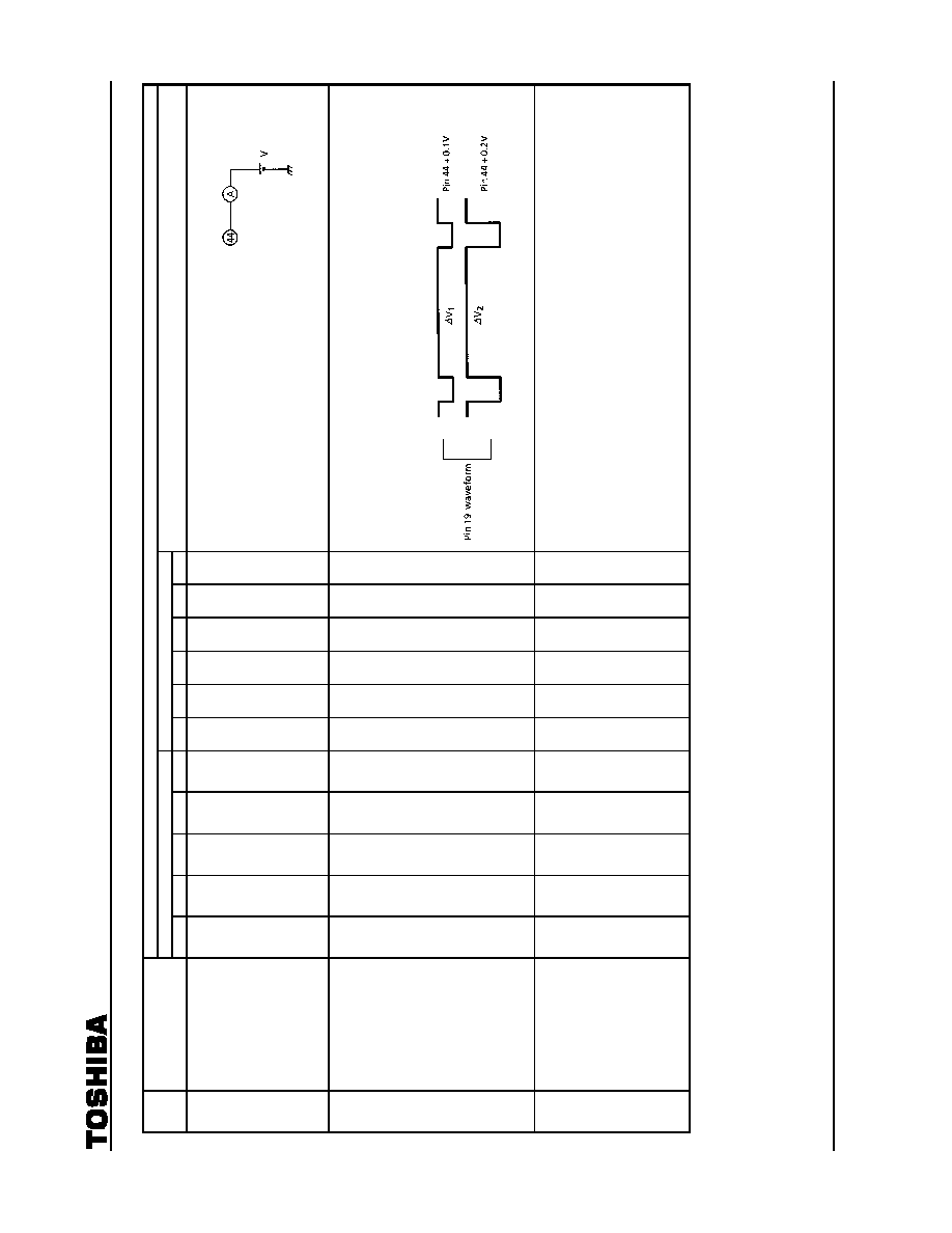
the current (Iin) at that time.
Zo44
() = 0.1V˜Iin (A)
Y
9
DC Transmission
Compensation Amplifier
Gain
Vari-
able
(1) Set the bus data so that DC transmission factor correction gain is maximum.
(2) In the condition of the Note Y
8
, observe Y
1out
waveform at pin 37 and measure
voltage change in the video period.
(3) Set the bus data so that DC transmission factor correction gain is centered, and
measure voltage in the same manner as the above step 2.
Adr = (V
2
- V
1
)˜0.1V˜Y
1
gain
Y
10
Maximum Gain of Black
Expansion Amplifier
A B
00H
E3H
(1) Set the bus data so that black expansion is on and black expansion point is
maximum.
(2) Input TG7 sine wave signal whose frequency is 500kHz and video amplitude is
0.1V to pin 45 (Y
1
IN).
(3) While impressing 1.0V to pin 39 (Black Peak Hold), measure amplitude (Va) of
Y
1out
signal at pin 37.
(4) While impressing 3.5V to pin 39 (Black Peak Hold), measure amplitude (Vb) of
Y
1out
signal at pin 37.
Akc
=
Va˜Vb

TB1227CNG
2004-05-24
39
TEST CONDITION (Unless otherwise specified : H, RGB V
CC
= 9V ; V
DD
, Fsc V
DD
, Y / C V
CC
= 5V ; Ta = 25±3∞C)
SW MODE
SUB-ADDRESS & BUS DATA
NOTE ITEM
S
39
S
42
S
44
S
45
S
51
04H 08H 0FH 10H 13H 14H
MEASURING METHOD
(1) Set the bus data so that black expansion is on and black expansion point is
maximum.
(2) Supply 1.0V to pin 39 (Black Peak Hold).
(3) Supply 2.9V to the APL of pin 44.
(4) Connect the power supply to pin 45
(Y
1
IN). While raising the supply
voltage from the level measured in the
preceding item Y
1
, measure voltage
change at pin 37 (Y
1out
).
(5) Set the bus data to center the black
expansion point, and perform the
same measurement as the above
steps 2 through 4.
Y
11
Black Expansion Start
Point
A C A A A
20H 04H 00H 00H BAH Vari-
able
(6) Set the black expansion point to the minimum by setting the bus data, and perform
the same measurement as the above steps 2 through 4.
(7) While supplying 2.2V to the APL of pin 44, perform the same measurement as the
above step 4 with the black expansion point set to maximum, center and minimum.
Y
12
Black Peak Detection
Period (Horizontal)
Black Peak Detection
Period (Vertical)
B
E3H
In the condition of the Note Y
1
, measure waveform at pin 39 (Black Peak Hold).
TB1227CNG
2004-05-24
40
TEST CONDITION (Unless otherwise specified : H, RGB V
CC
= 9V ; V
DD
, Fsc V
DD
, Y / C V
CC
= 5V ; Ta = 25±3∞C)
SW MODE
SUB-ADDRESS & BUS DATA
NOTE ITEM
S
39
S
42
S
44
S
45
S
51
04H 08H 0FH 10H 13H 14H
MEASURING METHOD
Y
13
Picture Quality Control
Peaking Frequency
A C A B A
3FH 04H 80H 00H BAH
Vari-
able
(1) Set the bus data so that picture quality control frequency is 2.5MHz.
(2) Input TG7 sine wave (sweeper) signal whose video level is 0.1V to pin 45 (Y
1
IN)
and pin 51 (Sync. IN).
(3) Maximize the picture quality control data.
(4) While
observing
Y
1out
of pin 37, find an SG frequency as the waveform amplitude
is maximum (fp25).
(5) Set the bus data so that picture quality control frequency is 3.1MHz and 4.2MHz,
and perform the same measurement as the above steps 2 through 4 at the
respective frequencies (fp31, fp42).
Y
14
Picture Quality Control
Maximum
Characteristic
(1) Input TG7 sine wave (sweeper) signal whose video level is 0.1V to pin 45 (Y
1
IN)
and pin 51 (Sync. IN).
(2) Set the picture quality control data to maximum.
(3) Set the picture quality control frequency is 2.5MHz by setting the bus data.
(4) Measure amplitude (V100k) of the output of pin 37 (Y
1
OUT) as the SG frequency
is 100kHz, and the amplitude (Vp25) of the same as the SG frequency is 2.5MHz.
GS25MX = 20og (Vp25 / V100k)
(5) Set the picture quality control frequency data to 3.1MHz by setting the bus data.
(6) Measure amplitude (V100k) of the output of pin 37 (Y
1
OUT) as the SG frequency
is 100kHz, and the amplitude (Vp31) of the same as the SG frequency is 3.1MHz.
GS31MX = 20og (Vp31 / V100k)
(7) Set the picture quality control frequency to 4.2MHz by setting the bus data.
(8) Measure amplitude (V100k) of the output of pin 37 (Y
1
OUT) as the SG frequency
is 100kHz, and the amplitude (Vp42) of the same as the SG frequency is 4.2MHz.
GS42MX = 20og (Vp42 / V100k)

TB1227CNG
2004-05-24
41
TEST CONDITION (Unless otherwise specified : H, RGB V
CC
= 9V ; V
DD
, Fsc V
DD
, Y / C V
CC
= 5V ; Ta = 25±3∞C)
SW MODE
SUB-ADDRESS & BUS DATA
NOTE ITEM
S
39
S
42
S
44
S
45
S
51
04H 08H 0FH 10H 13H 14H
MEASURING METHOD
Y
15
Picture Quality
Control Minimum
Characteristic
A C A B A
00H 04H 80H 00H BAH Vari-
able
(1) In the condition of the Note Y
14
, set the picture quality control bus data to
minimum.
(2) Perform the same measurement as the steps 3 through 8 of the Note Y
14
to find
respective gains as the picture quality control frequency is set to 2.5MHz, 3.1MHz
and 4.2MHz.
GS25MN = 20og (Vp25 / V100k)
GS31MN = 20og (Vp31 / V100k)
GS42MN = 20og (Vp42 / V100k)
Y
16
Picture Quality
Control Center
Characteristic
20H
(1) In the condition of the Note Y
14
, set the picture quality control bus data to center.
(2) Perform the same measurement as the steps 3 through 8 of the Note Y
14
to find
respective gains as the picture quality control frequency is set to 2.5MHz, 3.1MHz
and4.2MHz.
GS25CT = 20og (Vp25 / V100k)
GS31CT = 20og (Vp31 / V100k)
GS42CT = 20og (Vp42 / V100k)
Y
17
Y
Signal
Gain
03H
(1) Set the bus data so that black expansion is off, picture quality control is off and DC
transmission compensation is minimum.
(2) Input TG7 sine wave signal whose frequency is 100kHz and video level is 0.5V to
pin 45 (Y
1
IN) and pin 51 (Sync. IN). (Vyi100)
(3) Measure amplitude of Y
1
output at pin 37 (Vyout).
Gy
=
20og (Vyout / Vyi100)
Y
18
Y Signal Frequency
Characteristic
(1) Set the bus data so that black expansion is off, picture quality control is off and DC
transmission compensation is minimum.
(2) Input TG7 sine wave signal whose frequency is 6MHz and video level is 0.5V to pin
45 (Y
1
IN) and pin 51 (Sync. IN). (Vyi6M)
(3) Measure amplitude of Y
1
output at pin 37 (Vyo6M).
Gy6M
=
20og (Vyo6M / Vyi6M)
(4) Find Gfy from the result of the Note Y
17
.
Gfy = Gy6M - Gy

TB1227CNG
2004-05-24
42
TEST CONDITION (Unless otherwise specified : H, RGB V
CC
= 9V ; V
DD
, Fsc V
DD
, Y / C V
CC
= 5V ; Ta = 25±3∞C)
SW MODE
SUB-ADDRESS & BUS DATA
NOTE ITEM
S
39
S
42
S
44
S
45
S
51
04H 08H 0FH 10H 13H 14H
MEASURING METHOD
Y
19
Y Signal Maximum
Input Range
A C A B A
20H 04H 80H 00H BAH 03H
(1) Set the bus data so that black expansion is off, picture quality control is off and DC
transmission compensation is minimum.
(2) Input TG7 sine wave signal whose frequency is 100kHz to pin 45 (Y
1
IN) and pin
51 (Sync. IN).
(3) While increasing the amplitude Vyd of the signal in the video period, measure Vyd
just before the waveform of Y
1
output (pin 37) is distorted.
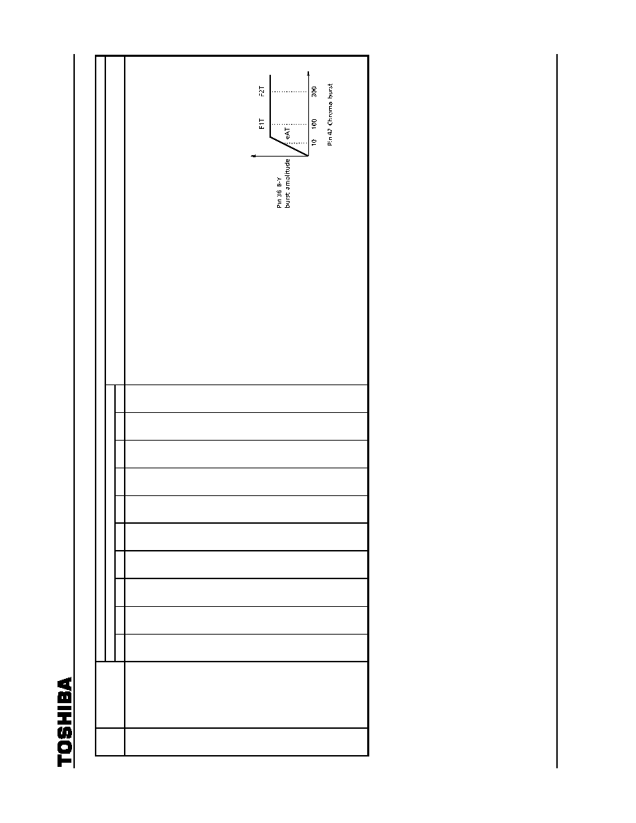
TB1227CNG
2004-05-24
43
TEST CONDITION (Unless otherwise specified : H, RGB V
CC
= 9V ; V
DD
, Fsc V
DD
, Y / C V
CC
= 5V ; Ta = 25±3∞C)
SW MODE
NOTE ITEM
S
26
S
1
S
31
S
33
S
34
S
39
S
42
S
44
S
45
S
51
MEASURING METHOD
(1) Activate the test mode (S26-ON, Sub Add 02 ; 01h).
(2) Set as follows : band pass filter Q = 2, f
o
= 600kHz, crystal clock = conforming to
European, Asian system.
(3) Set the gate to the normal status.
(4) Input 3N rainbow color bar signal to pin 42 (Chroma IN).
(5) When input signal to pin 42 is the same in the burst and chroma levels (10mV
p-p
), burst
amplitude of B-Y output signal from pin 36 is expressed as eAT. When the level of input
signal to pin 42 is 100mV
p-p
or 300mV
p-p
, burst amplitude of the B-Y output signal is
expressed as F1T or F2T. The ratio between F1T and F2T is expressed as AT.
F2T / F1T = AT
(6) Perform the same measurement in the
EXT. mode (f
o
= 0).
(eAE,
F1E,
AE)
C
1
ACC
Characteristic
ON A B B B A A A A B
(7) Input 4N rainbow color bar signal to pin 42 (Chroma IN), and perform the same
measurement as the above-mentioned steps with 3N rainbow color bar signal input.

TB1227CNG
2004-05-24
44
TEST CONDITION (Unless otherwise specified : H, RGB V
CC
= 9V ; V
DD
, Fsc V
DD
, Y / C V
CC
= 5V ; Ta = 25±3∞C)
SW MODE
NOTE ITEM
S
26
S
1
S
31
S
33
S
34
S
39
S
42
S
44
S
45
S
51
MEASURING METHOD
C
2
Band Pass Filter
Characteristic
ON A B B B A B A A B
(1) Activate the test mode (S26-ON, Sub Add 02 ; 01h).
(2) Set as follows : band pass filter Q = 2, crystal clock = conforming to 3.579 / 4.43MHz,
gate = normal status.
(3) Input 3N composite sine wave signal (1V
p-p
) to pin 42 (Chroma IN).
(4) Measure frequency characteristic of B-Y output of pin 36 and measure the peak
frequency, too.
(5) Changing
f
o
to 0, 500, 600 and 700 by the bus control and measure peak frequencies
respectively with different f
o
.
(6) For measuring frequency characteristic as f
o
is 4.43, use 4.43MHz crystal clock
Measure the following items in the same manner.

TB1227CNG
2004-05-24
45
TEST CONDITION (Unless otherwise specified : H, RGB V
CC
= 9V ; V
DD
, Fsc V
DD
, Y / C V
CC
= 5V ; Ta = 25±3∞C)
SW MODE
NOTE ITEM
S
26
S
1
S
31
S
33
S
34
S
39
S
42
S
44
S
45
S
51
MEASURING METHOD
C
3
Band Pass Filter,
-3dB Band
Characteristic
ON A B B B A B A A B
(1) Activate the test mode (S26-ON, Sub Add 02 ; 01h).
(2) Set as follows : band pass filter Q = 2, crystal clock = conforming to 3.579 / 4.43MHz.
(3) Set the gate to the normal status.
(4) Input 3N composite sine wave signal (1V
p-p
) to pin 42 (Chroma IN).
(5) Measure frequency characteristic of B-Y output of pin 36, and measure peak frequency
in the -3dB band.
(6) Changing
f
o
to 0, 500, 600 and 700 by the bus control and measure peak frequencies in
the -3dB band respectively with different f
o
.
C
4
Band Pass Filter,
Q Characteristic
Check
(1) Activate the test mode (S26-ON, Sub Add 02 ; 01h).
(2) Set as follows : TV mode (f
o
= 600), Crystal mode = conforming to 3.579 / 4.43MHz,
gate = normal status.
(3) Input 3N composite sine wave signal (1V
p-p
) to pin 42 (Chroma IN).
(4) Measure frequency characteristic of B-Y output of pin 36, and measure peak frequency
in the -3dB band.
(5) Changing
f
o
of the band pass filter to 0, 500, 600 and 700 by the bus control and
measure peak frequencies in the -3dB band respectively with different f
o
.

TB1227CNG
2004-05-24
46
TEST CONDITION (Unless otherwise specified : H, RGB V
CC
= 9V ; V
DD
, Fsc V
DD
, Y / C V
CC
= 5V ; Ta = 25±3∞C)
SW MODE
NOTE ITEM
S
26
S
1
S
31
S
33
S
34
S
39
S
42
S
44
S
45
S
51
MEASURING METHOD
C
5
1 / 2 f
o
Trap
Characteristic
ON A B B B A B A A B
(1) Activate the test mode (S26-ON, Sub Add 02 ; 01h).
(2) Set as follows : band pass filter Q = 2, crystal clock = conforming to 3.579 / 4.43MHz,
gate = normal status.
(3) Input 3N composite sine wave signal (1V
p-p
) to pin 42 (Chroma IN).
(4) Measure frequency characteristic of B-Y output of pin 36, and measure bottom
frequency.
(5) Changing
f
o
to 0, 500, 600 and 700 by the bus control and measure bottom frequencies
respectively with different f
o
.

TB1227CNG
2004-05-24
47
TEST CONDITION (Unless otherwise specified : H, RGB V
CC
= 9V ; V
DD
, Fsc V
DD
, Y / C V
CC
= 5V ; Ta = 25±3∞C)
SW MODE
NOTE ITEM
S
26
S
1
S
31
S
33
S
34
S
39
S
42
S
44
S
45
S
51
MEASURING METHOD
(1) Activate the test mode (S26-ON, Sub Add 02 ; 08h).
(2) Connect band pass filter (Q = 2), set crystal mode to conform to European, Asian
system and set the gate to normal status.
(3) Input 3N rainbow color bar signal (100mV
p-p
) to pin 42 (Chroma IN).
(4) Measure phase shift of B-Y color difference output of pin 36.
(5) While shifting color phase (tint) from minimum to maximum by the bus control, measure
phase change of B-Y color difference output of pin 36. On the condition that 6 bars in
the center have the peak level (regarded as center of color phase), the side of 5 bars is
regarded as positive direction while the side of 7 bars is regarded as negative direction
C
6
Tint Control
Sharing Range
(f
o
= 600kHz)
ON A B B B A A A A B
when the 5 bars or the 7 bars are in the peak level.
Based on this assumption,open angle toward the
positive direction is expressed as
1
and that
toward the negative direction is expressed as
2
as
viewed from the phase center.
1
and
2
show
the tint control sharing range.
(6) Variable range is expressed by sum of
1
sharing
range and
2
sharing range.
T
=
1
+
2
C
7
Tint Control
Variable Range
(f
o
= 600kHz)
(7) While shifting color phase from minimum to maximum with the bus control, measure
phase shift of B-Y color difference output of pin 36. When center 6 bars have peak level,
value of color phase bus step is expressed as
Tin
.
(8) While shifting color phase from minimum to maximum with the bus control, measure
values of color phase bus step corresponding to 10% and 90% of absolutely variable
phase shift of B-Y color difference output of pin36.
The range of color phase shifted by the bus control is
expressed as While shifting color phase from
minimum to maximum with the bus control, measure
phase shift of B-Y color difference output of pin 36.
When center 6 bars have peak level, value of color
phase bus step is expressed as
Tin
(conforming to
TV mode, f
o
= 600kHz).
C
8
Tint Control
Characteristic
(9) Input 4N rainbow color bar signal to pin 42 (Chroma IN), and perform the same
measurement as the 3N signal.

TB1227CNG
2004-05-24
48
TEST CONDITION (Unless otherwise specified : H, RGB V
CC
= 9V ; V
DD
, Fsc V
DD
, Y / C V
CC
= 5V ; Ta = 25±3∞C)
SW MODE
NOTE ITEM
S
26
S
1
S
31
S
33
S
34
S
39
S
42
S
44
S
45
S
51
MEASURING METHOD
C
9
APC Lead-In
Range
OFF
ON
A B B B A
A
C
A A B
(1) Connect band pass filter (Q = 2), set to TV mode (f
o
= 600kHz) with X'tal clock
conforming to European, Asian system.
(2) Set the gate to normal status.
(3) Input 3N CW signal of 100mV
p-p
to pin 42 of the chroma input terminal.
(4) While changing frequency of the CW (continuous waveform) signal, measure its
frequency when B-Y color difference signal of pin 36 is colored.
(5) Input 4N CW (continuous waveform) 100mV
p-p
signal to pin 42 (Chroma IN).
(6) While changing frequency of the CW signal, measure frequencies when B-Y color
difference output of pin 36 is colored and discolored. Find difference between the
measured frequency and f
c
(4.433619MHz) and express the differences as fPH and
fPL, which show the APC lead-in range.
(7) Variable frequency of VCXO is used to cope with lead-in of 3.582MHz / 3.575MHz PAL
system.
(8) Activate the test mode (S26-ON, Sub Add 02 ; 02h).
(9) Input nothing to pin 42 (Chroma IN).
(10) While varying voltage of pin 30 (APC Filter), measure variable frequency of VCXO at pin
35 (R-Y OUT) while observing color and discoloring of R-Y color difference signal.
Express difference between the high frequency (fH) and f
o
center as 3.582HH, and
difference between the low frequency (fL) and f
o
center as 3.582HL. Perform the same
measurement for the NP system (3.575MHz PAL).
C
10
APC Control
Sensitivity
ON
C
(1) Activate the test mode (S26-ON, Sub Add 02 ; 02h).
(2) Connect band pass filter as same as the Note C
9
.
(3) Change the X'tal mode properly to the system.
(4) Input nothing to pin 42 (Chroma IN).
(5) When
V
30
's APC voltage ±50mV is impressed to pin 30 (APC Filter) while its voltage is
being varied, measure frequency change of pin 35 output signal as frH or frL and
calculate sensitivity according to the following equation.
b
=
(frH
- frL) / 100

TB1227CNG
2004-05-24
49
TEST CONDITION (Unless otherwise specified : H, RGB V
CC
= 9V ; V
DD
, Fsc V
DD
, Y / C V
CC
= 5V ; Ta = 25±3∞C)
SW MODE
NOTE ITEM
S
26
S
1
S
31
S
33
S
34
S
39
S
42
S
44
S
45
S
51
MEASURING METHOD
C
11
Killer Operation
Input Level
OFF
A B B B A A A A B
(1) Connect band pass filter (Q = 2) and set to TV mode (f
o
= 600kHz).
(2) Set the crystal mode to conform to European, Asian system and set the gate to normal
status.
(3) Input 3N color signal having 200mV
p-p
burst to pin 42 (Chroma IN).
(4) While attenuating chroma input signal, measure input burst amplitudes of the signal
when B-Y color difference output of pin 36 is discolored and when the same signal is
colored. Measured input burst amplitudes shall be expressed as 3N-VTK1 and
3N-VTC1 respectively (killer operation input level).
(5) Killer operation input level in the condition that P / N killer sensitivity is set to LOW with
the bus control is expressed as 3N-VTK2 or 3N-VTC2.
(6) Perform the same measurement as the above step 4 with different inputs of 4N, 4P, MP,
NP color signals having 200mV
p-p
burst to pin 42 (Chroma IN). (When measuring with
MP / NP color signal, set the crystal system to conform to South American system.)
(7) Killer operation input level at that time is expressed as follows.
Normal killer operation input level in the 4N system is expressed as 4N-VTK1,
4N-VTC1.
Normal killer operation input level in the 4P system is expressed as 4P-VTK1, 4P-VTC1.
Killer operation input level with low killer sensitivity is expressed as 4P-VTK2, 4P-VTC2.
Normal killer operation input level in the MP system is expressed as MP-VTK2,
MP-VTC2.
Normal killer operation input level in the NP system is expressed as NP-VTK1,
NP-VTC1.
Killer operation input level with low killer sensitivity is expressed as NP-VTK2,
NP-VTC2.
[Reference] 3N system : 3.579545MHz
NTSC
4N system : 4.433619MHz
False NTSC
4P system : 4.433619MHz
PAL
MP system : 3.575611MHz
M-PAL
NP system : 3.582056MHz
N-PAL

TB1227CNG
2004-05-24
50
TEST CONDITION (Unless otherwise specified : H, RGB V
CC
= 9V ; V
DD
, Fsc V
DD
, Y / C V
CC
= 5V ; Ta = 25±3∞C)
SW MODE
NOTE ITEM
S
26
S
1
S
31
S
33
S
34
S
39
S
42
S
44
S
45
S
51
MEASURING METHOD
C
12
Color
Difference
Output
ON A B B B A A A A B
(1) Activate the test mode (S26-ON, Sub Add 02 ; 08h).
(2) Connect band pass filter (Q = 2), set to TV mode (f
o
= 600kHz) with 0dB attenuation.
(3) Set the crystal mode to conform to European, Asian system and set the gate to normal
status.
(4) Input 3N, 4N and 4P rainbow color bar signals having 100mV
p-p
burst to pin 42 of the
chroma input terminal one after another.
(5) Measure amplitudes of color difference signals of pin 36 (B-Y) and pin 35 (R-Y)
respectively, and express them as 3NeB-Y / R-Y, 4NeB-Y / R-Y and 4PeB-Y / R-Y
respectively.
(6) While inputting 4P 75% color bar signal (100mV
p-p
burst) to pin 42 of the chroma input
terminal, measure amplitudes of color difference signals of pin 36 (B-Y OUT) and pin 35
(R-Y OUT) respectively. (Ratio of those amplitudes is expressed as 4Peb-y / r-y for
checking color level of SECAM system.)
C
13
Demodulation
Relative
Amplitude
(1) Activate the test mode (S26-ON, Sub Add 02 ; 08h).
(2) Connect band pass filter (Q = 2), set to TV mode (f
o
= 600kHz) with 0dB attenuation.
(3) Set the crystal mode to conform to European, Asian system and set the gate to normal
status.
(4) Input 3N, 4N and 4P rainbow color bar signals having 100mV
p-p
burst to pin 42 of the
chroma input terminal one after another.
(5) Measure amplitudes of color difference signals of pin 36 (B-Y) and pin 35 (R-Y)
respectively, and express ratio between the two amplitudes as 3NG R / B, 4NG R / B
and 4PG R / B respectively.
(Note) Relative amplitude of G-Y color difference signal shall be checked later in the
Text
section.

TB1227CNG
2004-05-24
51
TEST CONDITION (Unless otherwise specified : H, RGB V
CC
= 9V ; V
DD
, Fsc V
DD
, Y / C V
CC
= 5V ; Ta = 25±3∞C)
SW MODE
NOTE ITEM
S
26
S
1
S
31
S
33
S
34
S
39
S
42
S
44
S
45
S
51
MEASURING METHOD
C
14
Demodulation
Relative Phase
ON A B B B A A A A B
(1) Activate the test mode (S26-ON, Sub Add 02 ; 08h).
(2) Connect band pass filter (Q = 2), set to TV mode (f
o
= 600kHz) with 0dB attenuation.
(3) Set the crystal mode to conform to European, Asian system and set the gate to normal
status.
(4) Input 3N, 4N and 4P rainbow color bar signals having 100mV
p-p
burst to pin 42 of the
chroma input terminal one after another.
(5) Measure phases of color difference signals of pin 36 (B-Y) and pin 35 (R-Y)
respectively, and express them as 3NR-B, 4NR-B and 4PR-B respectively.
(6) For measuring with 3N and 4N color bar signals in NTSC system, set six bars of the B-Y
color difference waveform to the peak level with the Tint control and measure its phase
difference from phase of R-Y color difference signal of pin 35 (R-Y OUT).
(Note) Relative phase of G-Y color difference signal shall be checked later in the Text
section.
C
15
Demodulation
Output Residual
Carrier
(1) Activate the test mode (S26-ON, Sub Add 02 ; 08h).
(2) Connect band pass filter (Q = 2), set to TV mode (f
o
= 600kHz) with 0dB attenuation.
(3) Set the crystal mode to conform to European, Asian system.
(4) Set the gate to normal status.
(5) Input 3N and 4N rainbow color bar signals having 100mVp-p burst to pin 42 of the
chroma input terminal one after another.
(6) Measure subcarrier leak of 3N and 4N color bar signals appearing in color difference
signals of pin 36 (B-Y OUT) and pin 35 (R-Y OUT) respectively, and express those
leaks as 3N-SCB / R and 4N-SCB / R.

TB1227CNG
2004-05-24
52
TEST CONDITION (Unless otherwise specified : H, RGB V
CC
= 9V ; V
DD
, Fsc V
DD
, Y / C V
CC
= 5V ; Ta = 25±3∞C)
SW MODE
NOTE ITEM
S
26
S
1
S
31
S
33
S
34
S
39
S
42
S
44
S
45
S
51
MEASURING METHOD
C
16
Demodulation
Output Residual
Higher Harmonic
ON A B B B A A A A B
(1) Activate the test mode (S26-ON, Sub Add 02 ; 08h).
(2) Connect band pass filter (Q = 2), set to TV mode (f
o
= 600kHz) with 0dB attenuation.
(3) Set the crystal mode to conform to European, Asian system and set the gate to normal
status.
(4) Input 3N and 4N rainbow color bar signals having 100mV
p-p
burst to pin 42 of the
chroma input terminal one after another.
(5) Measure higher harmonic (2f
c
= 7.16MHz or 8.87MHz) of 3N and 4N color bar signals
appearing in color difference signals of pin 36 (B-Y OUT) and pin 35 (R-Y OUT)
respectively, and express them as 3N-HCB / R and 4N-HCB / R.
C
17
Color Difference
Output ATT
Check
(1) Activate the test mode (S26-ON, Sub Add 02 ; 08h).
(2) Connect band pass filter (Q = 2) and set bus data for the TV mode (f
o
= 600kHz).
(3) Set the X'tal clock mode to conform to European, Asian system and set the gate to
normal status.
(4) Input 3N rainbow color bar signal whose burst is 100mV
p-p
to pin 42 of the chroma input
terminal.
(5) Measure amplitude of color difference output signal of pin 36 (B-Y OUT) with 0dB
attenuation set by the bus control. Set the amplitude of the color difference output of pin
36 (B-Y OUT) to 0dB, and measure amplitude of the same signal with different
attenuation of -2dB, -1dB and +1dB set by the bus control.

TB1227CNG
2004-05-24
53
TEST CONDITION (Unless otherwise specified : H, RGB V
CC
= 9V ; V
DD
, Fsc V
DD
, Y / C V
CC
= 5V ; Ta = 25±3∞C)
BUS : TEST MODE
BUS : NORMAL CONTROL MODE
S 02H
07H
10H
NOTE ITEM
26 D
5
D
2
D
1
D
0
D
7
D
4
D
3
D
5
D
4
D
3
D
2
D
1
D
0
OTHER CONDITION
MEASURING METHOD
C
18
16.2MHz Oscillation
Frequency
ON 0 0 0 1
0
0
0
0
0
0
0
0
0
--
(1) Input nothing to pin 42.
(2) Measure frequency of CW signal of pin 35 as fr, and find
oscillation frequency by the following equation.
foF = (fr - 0.05MHz)◊4
C
19
16.2MHz Oscillation
Start Voltage
ON 0 0 0 1
0
0
0
0
0
0
0
0
0
Impress pin 38
individually with
separate power supply.
While raising voltage of pin 38, measure voltage when
oscillation waveform appears at pin 40.
C
20
f
sc
Free-Run
Frequency
ON 0 0 0 1
0
0
0
0
Variable 0
0
--
(1) Input nothing to pin 42.
(2) Change setting of SUB (10H) D
4
, D
3
and D
2
according to
respective frequency modes, and measure frequency of
CW signal of pin 35.
Detail of D
4
, D
3
and D
2
3.58M = 1 : (001), 4.43M = 2 : (010)
M-PAL = 6 : (110), N-PAL = 7 : (111)
C
21
f
sc
Output
Amplitude OFF 0 0 0 0
0
0
0
0
0
1
0
1
0
0
0
--
(1) Input nothing to pin 42.
(2) Change setting of SUB (10H) D
4
, D
3
and D
2
according to
respective frequency modes.Measure the amplitude of
output signal of pin 27.

TB1227CNG
2004-05-24
54
DEF SECTION
TEST CONDITION
Unless otherwise specified : H, RGB V
CC
= 9V ; V
DD
, Fsc V
DD
, Y / C V
CC
= 5V ; Ta = 25±3∞C ; BUS = preset value ;
pin 51 input video signal = 50 system
(Note) "◊" in the data column represents preset value at power ON.
NOTE ITEM
SUB-ADDRESS & BUS DATA
MEASURING METHOD
DH1 H. Reference
Frequency
Sub 02H
0
0
0
0
0
0
0
1
(1) Supply 5V to pin 26.
(2) Set bus data as indicated on the left.
(3) Measure the frequency of sync. output of pin 49.
DH2
H. Reference
Oscillation Start
Voltage
Sub 02H
0
0
0
0
0
0
0
1
In the test condition of the Note DH1, turning down the voltage supplied to pin 26 from 5V, measure the voltage
when oscillation of pin 49 stops.
DH3 H. Output
Frequency 1
Sub 10H
◊
◊
◊
◊
◊
◊
0
1
(1) Set bus data as indicated on the left.
(2) In the condition of the above step 1, measure frequency (TH1) at pin 4.
DH4 H. Output
Frequency 2
Sub 10H
◊
◊
◊
◊
◊
◊
1
0
(1) Set the input video signal of pin 51 to the 60 system.
(2) Set bus data as indicated on the left.
(3) In the above-mentioned condition, measure frequency (TH2) at pin 4.
DH5 H. Output Duty 1
--
--
--
--
--
--
--
--
--
(1) Supply 4.5V DC to pin 5 (or, make pin 5 open-circuited).
(2) Measure duty of pin 4 output.
DH6 H. Output Duty 2
--
--
--
--
--
--
--
--
--
(1) Make a short circuit between pin 5 and ground.
(2) Measure duty of pin 4 output.
DH7 H. Output Duty
Switching Voltage
-- --
--
--
--
--
--
--
-- Supply 2V DC to pin 5. While turning down the voltage from 2V, measure voltage when the output duty ratio
becomes 41 to 37%.
DH8 H.
Output
Voltage
--
-- -- --
--
--
--
--
--
Measure the low voltage and high voltage of pin 4 output whose waveform is shown below.
DH9 H. Output Oscillation
Start Voltage
--
--
--
--
--
--
--
--
-- While raising H. V
CC
(pin 3) from 0V, measure voltage when pin 4 starts oscillation.
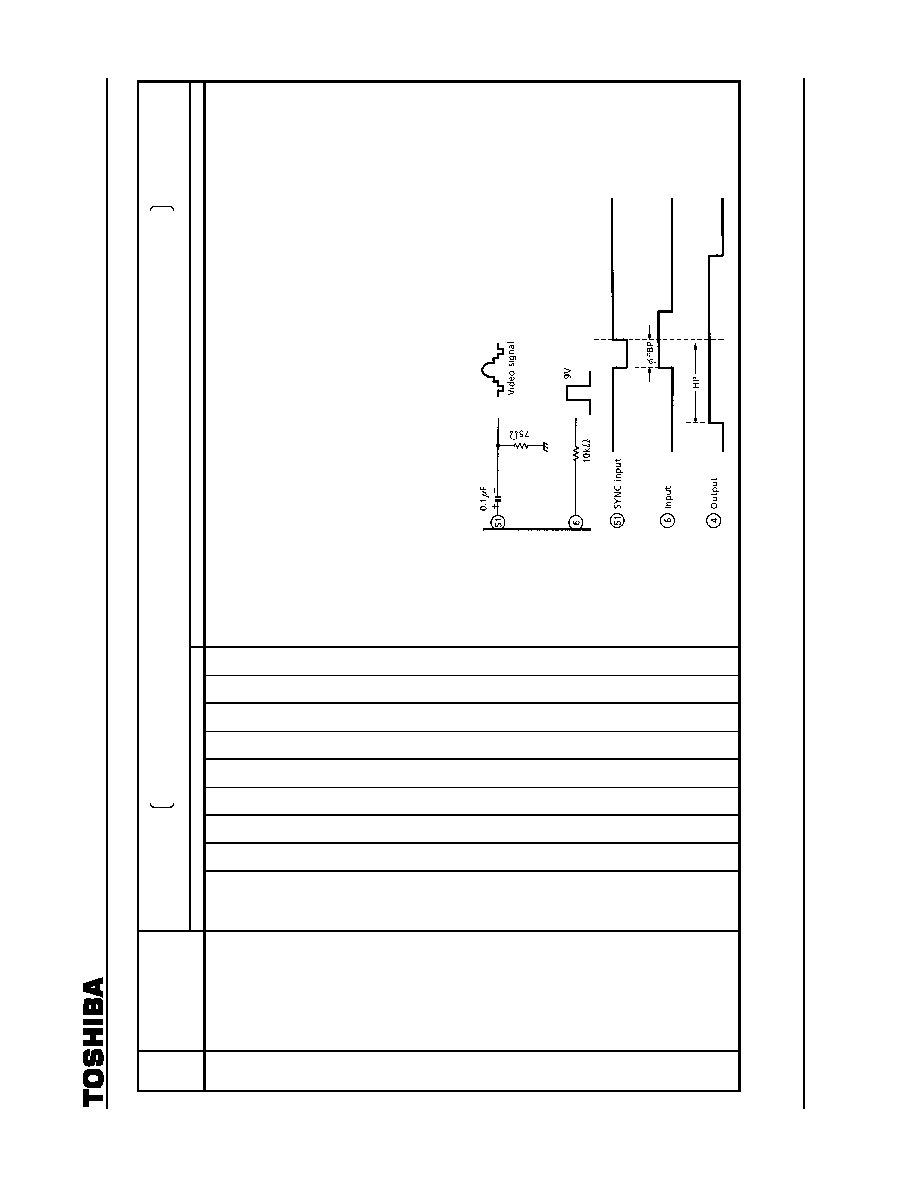
TB1227CNG
2004-05-24
55
TEST CONDITION
Unless otherwise specified : H, RGB V
CC
= 9V ; V
DD
, Fsc V
DD
, Y / C V
CC
= 5V ; Ta = 25±3∞C ; BUS = preset value ;
pin 51 input video signal = 50 system
(Note) "◊" in the data column represents preset value at power ON.
NOTE ITEM
SUB-ADDRESS & BUS DATA
MEASURING METHOD
DH10 H. FBP Phase
DH11 H. Picture Position,
Maximum
DH12 H. Picture Position,
Minimum
DH13 H. Picture position
Control Range
DH14 H.
Distortion
Correction Control
Range
Sub 0BH
0
1
0
1
0
1
0
1
0
1
◊
◊
◊
◊
◊
◊
(1) Supply 4.5V DC to pin 5.
(2) Input video signal to pin 51.
(3) Set the width of pin 6 input pulse to 8µs.
(4) Measure
FBP shown in the figure below (FBP).
(5) Adjust the phase of pin 6 input pulse so that the center of pin 4's output pulse corresponds to the trailing
edge of input sync. signal.
(6) Set bus data as indicated on the left and measure the horizontal picture position with respective bus data
settings (HSFTmax, HSFTmin).
(7) Find HP difference between the conditions mentioned in the above step 6 (HSFT).
(8) Reset bus data to the preset value.
(9) While impressing 5V DC to pin 5, measure HP.
(10) While impressing 4V DC to pin 5, measure HP.
(11) Find difference between the two measurement results obtained in the preceding steps 9 and 10 (HCC).

TB1227CNG
2004-05-24
56
TEST CONDITION
Unless otherwise specified : H, RGB V
CC
= 9V ; V
DD
, Fsc V
DD
, Y / C V
CC
= 5V ; Ta = 25±3∞C ; BUS = preset value ;
pin 51 input video signal = 50 system
(Note) "◊" in the data column represents preset value at power ON.
NOTE ITEM
SUB-ADDRESS & BUS DATA
MEASURING METHOD
DH15 H.
BLK
Phase
Sub02H 0 0 0
0
0
1
0
0
DH16 H.
BLK
Width,
Minimum
DH17 H.
BLK
Width,
Maximum
Sub 16H
0
1
0
1
0
1
◊
◊
◊
◊
◊
◊
◊
◊
◊
◊
(1) In the condition of the steps 1 through 4 of the Note DH10, perform the following measurement.
(2) Supply 5V DC to pin 26.
(3) Set bus data as indicated on the left.
(4) Measure phase difference between pin 51 and pin 49 as shown below.
(5) Change the bus data as shown on the left and measure BLK width.
DH18 P / N-GP Start
Phase 1
DH19 P / N-GP Start
Phase 2
DH20 P / N-GP Gate
Width 1
DH21 P / N-GP Gate
Width 2
Sub 0FH
◊
◊
◊
◊
◊
◊
◊
◊
0
1
◊
◊
◊
◊
◊
◊
(1) Supply 5V to pin 26.
(2) Set bus data as indicated on the left.
(3) With the respective bus data settings mentioned above, measure the phase and gate width as shown in
the figure below.
DH22 SECAM-GP Start
Phase 1
DH23 SECAM-GP Start
Phase 2
DH24 SECAM-GP Gate
Width 1
DH25 SECAM-GP
Gate
Width 2
Sub 1FH
◊
◊
◊
◊
◊
◊
0
1
◊
◊
◊
◊
◊
◊
◊
◊
(1) Supply 5V to pin 26.
(2) Set bus data as indicated on the left.
(3) With the respective bus data settings mentioned above, measure the phase and gate width as shown in
the figure below.

TB1227CNG
2004-05-24
57
TEST CONDITION
Unless otherwise specified : H, RGB V
CC
= 9V ; V
DD
, Fsc V
DD
, Y / C V
CC
= 5V ; Ta = 25±3∞C ; BUS = preset value ;
pin 51 input video signal = 50 system
(Note) "◊" in the data column represents preset value at power ON.
NOTE ITEM
SUB-ADDRESS & BUS DATA
MEASURING METHOD
DH26 Noise
Detection
Level 1
DH27 Noise
Detection
Level 2
DH28 Noise
Detection
Level 3
DH29 Noise
Detection
Level 4
Sub 1DH
0
0
1
1
0
1
0
1
◊
◊
◊
◊
◊
◊
◊
◊
◊
◊
◊
◊
◊
◊
◊
◊
◊
◊
◊
◊
◊
◊
◊
◊
(1) Input such a signal as shown by "a" of the following figure to pin 51.
(2) Set bus data as indicated in the first line of the left table.
(3) Measure NLX when amplitude of pin 41 changes. NL1
(4) Set bus data as indicated in the second line of the left table.
(5) Measure NLX when amplitude of pin 41 changes. NL2
(6) Set bus data as indicated in the third line of the left table.
(7) Measure NLX when amplitude of pin 41 changes. NL3
(8) Set bus data as indicated in the fourth line of the left table.
(9) Measure NLX when amplitude of pin 41 changes. NL4
DV1 V. Ramp Amplitude
-- --
--
--
--
--
--
--
--
(1) Measure amplitude of V. ramp waveform of pin 52.
DV2 V. NF Maximum
Amplitude
Sub 17H 1 1 1
1
1
1
1
◊
(1) Set data bus as indicated on the left.
(2) Measure amplitude of pin 54's signal.
DV3 V. NF Minimum
Amplitude
Sub 17H 0 0 0
0
0
0
0
◊
(1) Set data bus as indicated on the left.
(2) Measure amplitude of pin 54's signal.

TB1227CNG
2004-05-24
58
TEST CONDITION
Unless otherwise specified : H, RGB V
CC
= 9V ; V
DD
, Fsc V
DD
, Y / C V
CC
= 5V ; Ta = 25±3∞C ; BUS = preset value ;
pin 51 input video signal = 50 system
(Note) "◊" in the data column represents preset value at power ON.
NOTE ITEM
SUB-ADDRESS & BUS DATA
MEASURING METHOD
DV4 V.
Amplification
Degree
DV5 V.
Amplifier
Max.
Output
DV6 V.
Amplifier
Min.
Output
Sub
1BH
1 1 ◊
◊
◊
◊
◊
◊
(1) Set bus data as indicated on the left.
(2) Change 5.0V of pin 54 voltage by +0.1V and -0.1V, and measure V
53
output voltage in both the
conditions.
(3) Find GVA shown in the figure below.
(4) Measure Vvmax and Vvmin shown in the figure below.
DV7
V. S-Curve
Correction, Max.
Correction Quantity
Sub 19H 1 1 1
1
1
1
1
◊
(1) Adjust the oscilloscope's amplitude with the UNCAL so that pin 52 and pin 54 waveforms overlap each
other as the bus data is set to the preset value.
(2) Change the bus data as indicated on the left, and measure values of X and Y shown in the figure below.
(3) Find
V
S
according to the equation that V
S
= (X / Y)◊100%.

TB1227CNG
2004-05-24
59
TEST CONDITION
Unless otherwise specified : H, RGB V
CC
= 9V ; V
DD
, Fsc V
DD
, Y / C V
CC
= 5V ; Ta = 25±3∞C ; BUS = preset value ;
pin 51 input video signal = 50 system
(Note) "◊" in the data column represents preset value at power ON.
NOTE ITEM
SUB-ADDRESS & BUS DATA
MEASURING METHOD
DV8
V. Reverse S-Curve
Correction, Max.
Correction Quantity
Sub 19H 0 0 0
0
0
0
0
◊
(1) Adjust the oscilloscope's amplitude with the UNCAL so that pin 52 and pin 54 waveforms overlap each
other as the bus data is set to the preset value.
(2) Change the bus data as indicated on the left, and measure values of X and Y shown in the figure below.
(3) Find
V
S
according to the equation that V
S
= (X / Y)◊100%.
DV9 V. Linearity Max.
Correction Quantity
Sub 1AH 1 1
1
1
1
◊
◊
◊
(1) Adjust the oscilloscope's amplitude with the UNCAL so that pin 52 and pin 54 waveforms overlap each
other as the bus data is set to the preset value.
(2) Change the bus data as indicated on the left, and measure values of X and Y shown in the figure below.
(3) Find
V
S
according to the equation that V
S
= (X / 2Y)◊100%.

TB1227CNG
2004-05-24
60
TEST CONDITION
Unless otherwise specified : H, RGB V
CC
= 9V ; V
DD
, Fsc V
DD
, Y / C V
CC
= 5V ; Ta = 25±3∞C ; BUS = preset value ;
pin 51 input video signal = 50 system
(Note) "◊" in the data column represents preset value at power ON.
NOTE ITEM
SUB-ADDRESS & BUS DATA
MEASURING METHOD
DV10 AFC-MASK
Start
Phase
DV11 AFC-MASK
Stop
Phase
DV12 VNFB
Phase
Sub 02H
Sub 16H
0
◊
0
◊
0
◊
0
◊
0
◊
0
0
0
0
1
0
(1) Supply 5V DC to pin 26.
(2) Set bus data as indicated on the left and activate the test mode.
(3) Measure the AFC-MASK start phase (X) and AFC-MASK stop phase (Y) of pin 49.
(4) Set the Sub 16H as indicated on the left.
(5) Measure the VNFB start phase (Z) of pin 54.
DV13 V.
Output
Maximum
Phase
DV14 V.
Output
Minimum
Phase
DV15 V.
Output
Phase
Variable Range
Sub 16H
◊
◊
◊
◊
◊
◊
◊
◊
◊
◊
0
1
0
1
0
1
(1) Input video signal to pin 51.
(2) Measure both phases (Xmax, Xmin) of pin 52 and pin 54 with the respective bus data settings shown on
the left.
(3) Find difference between the two phases measured in the above step 2.
Y = Xmax - Xmin

TB1227CNG
2004-05-24
61
TEST CONDITION
Unless otherwise specified : H, RGB V
CC
= 9V ; V
DD
, Fsc V
DD
, Y / C V
CC
= 5V ; Ta = 25±3∞C ; BUS = preset value ;
pin 51 input video signal = 50 system
(Note) "◊" in the data column represents preset value at power ON.
NOTE ITEM
SUB-ADDRESS & BUS DATA
MEASURING METHOD
DV16 50 System VBLK
Start Phase
DV17 50 System VBLK Stop
Phase
Sub 1BH
Sub 1CH
0
0
1
◊
◊
◊
◊
◊
◊
◊
◊
◊
◊
◊
◊
◊
(1) Input such a video signal of the 50 system as shown in the figure to pin 51.
(2) Set bus data as indicated on the left.
(3) Measure the VBLK start phase (X) and VBLK stop phase (Y) of pin 12.
DV18 60 System VBLK
Start Phase
DV19 60 System VBLK Stop
Phase
Sub 1BH
Sub 1CH
0
0
1
◊
◊
◊
◊
◊
◊
◊
◊
◊
◊
◊
◊
◊
(1) Input such a video signal of the 60 system as shown in the figure to pin 51.
(2) Set bus data as indicated on the left.
(3) Measure the VBLK start phase (X) and VBLK stop phase (Y) of pin 12.
DV20 V. Lead-In Range 1
Sub 16H ◊
◊
◊
0
0
0
0
0
(1) Set bus data as indicated on the left.
(2) Input 262.5 H video signal to pin 51.
(3) Set a certain number of field lines in which signals of pin 51 and pin 54 completely synchronize with each
other as shown in the figure below.
(4) Decrease the field lines in number and measure number of lines in which pin 51 and pin 54 signals do not
synchronize with each other.
(5) Again set a certain number of field lines in which pin 51 and pin 52 signals synchronize with each other.
(6) Increase the field lines in number and measure number of lines in which pin 51 and pin 52 signals do not
synchronize with each other.

TB1227CNG
2004-05-24
62
TEST CONDITION
Unless otherwise specified : H, RGB V
CC
= 9V ; V
DD
, Fsc V
DD
, Y / C V
CC
= 5V ; Ta = 25±3∞C ; BUS = preset value ;
pin 51 input video signal = 50 system
(Note) "◊" in the data column represents preset value at power ON.
NOTE ITEM
SUB-ADDRESS & BUS DATA
MEASURING METHOD
DV21 V. Lead-In Range 2
Sub 16H ◊
◊
◊
0
1
0
0
0
(1) Set bus data as indicated on the left.
(2) Input 262.5 H video signal to pin 51.
(3) Set a certain number of field lines in which signals of pin 51 and pin 54 completely synchronize with each
other as shown in the figure below.
(4) Decrease the field lines in number and measure number of lines in which pin 51 and pin 54 signals do not
synchronize with each other.
(5) Again set a certain number of field lines in which pin 51 and pin 52 signals synchronize with each other.
(6) Increase the field lines in number and measure number of lines in which pin 51 and pin 52 signals do not
synchronize with each other.
DV22 W-VBLK Start Phase
DV23 W-PMUTE
Start
Phase
(Note) Only the 60
system is subject to
evaluation.
Sub 1BH
Sub 1DH
◊
◊
◊
◊
◊
◊
◊
◊
0
1
0
1
0
1
0
1
0
1
0
1
0
1
0
1
0
1
0
1
0
1
0
1
(1) Set bus data as specified for the Sub 1BH in the left columns, and measure the value of X shown in the
figure below.
W-VBLK start phase : MAX, MIN
(2) Set bus data as specified for the Sub 1DH in the left columns, and measure the value of X shown in the
figure below.
W-PMUTE start phase : MAX, MIN

TB1227CNG
2004-05-24
63
TEST CONDITION
Unless otherwise specified : H, RGB V
CC
= 9V ; V
DD
, Fsc V
DD
, Y / C V
CC
= 5V ; Ta = 25±3∞C ; BUS = preset value ;
pin 51 input video signal = 50 system
(Note) "◊" in the data column represents preset value at power ON.
NOTE ITEM
SUB-ADDRESS & BUS DATA
MEASURING METHOD
DV24 W-VBLK
Stop
Phase
DV25 W-PMUTE
Stop
Phase
(Note) Only the 60
system is subject to
evaluation.
Sub 1CH
Sub 1EH
◊
◊
◊
◊
0
1
0
1
0
1
0
1
0
1
0
1
0
1
0
1
0
1
0
1
0
1
0
1
0
1
0
1
(1) Set bus data as specified for the Sub 1CH in the left columns, and measure the value of Y shown in the
figure below.
W-VBLK stop phase : MAX, MIN
(2) Set bus data as specified for the Sub 1EH in the left columns, and measure the value of Y shown in the
figure below.
W-PMUTE stop phase : MAX, MIN
DV26 V Centering Center
Voltage
DV27 V
Centering
Max
Voltage
DV28 V
Centering
Min
Voltage
Sub 18H
1
1
0
0
1
0
0
1
0
0
1
0
0
1
0
0
1
0
◊
◊
◊
◊
◊
◊
(1) Set bus data as indicated on the left.
(2) Measure the voltage of pin 47 with respective bus data settings.

TB1227CNG
2004-05-24
64
1H DL SECTION
TEST CONDITION (Unless otherwise specified : H, RGB V
CC
= 9V ; V
DD
, Fsc V
DD
, Y / C V
CC
= 5V ; Ta = 25±3∞C ; BUS = preset value ;
pin3 = 9V ; pin8 ∑ 38 ∑ 41 = 5V)
SW MODE
SUB ADDRESS &
DATA
NOTE ITEM
S26 07H
0FH
11H
MEASURING METHOD
H
1
1HDL Dynamic
Range Direct
ON 94H
--
--
(1) Input waveform 1 to pin 33 (B ∑ Yin) , and measure VNBD,
that pin 36 (B ∑ Yout) is saturated input level.
(2) Measure VNRD of R ∑ Y input in the same way as VNBD.
H
2
1HDL Dynamic
Range Delay
8CH
--
--
(1) Input waveform 1 to pin 33 (B-Yin), and measure VPBD, that pin 36 (B-Yout) is saturated input level.
(2) Measure VPRD of R-Y input in the same way as VPBD.
H
3
1HDL Dynamic
Range,
Direct+Delay
A4H
--
--
(1) Input waveform 1 to pin 33 (B-Yin), and measure VSBD, that pin 36 (B-Yout) is saturated input level.
(2) Measure VNRD of R-Y input in the same way as VSBD.
H
4
Frequency
Characteristic,
Direct
94H
--
--
(1) In the same measuring as H
1
, set waveform 1 to 0.3V
p-p
and f = 100kHz. Measure VB100, that is pin 36 (B-Yout) level.
And set waveform 1 to f = 700kHz. Measure VB700, that is pin 36 (B-Yout) level.
GHB1 = 20og (VB700 / VB100)
(2) Measure GHR1 of R-Y out in the same way as GHB1.
H
5
Frequency
Characteristic,
Delay
8CH
--
--
(1) In the same measuring as H
1
, set waveform 1 to 0.3V
p-p
and f = 100kHz. Measure VB100, that is pin 36 (B-Yout) level.
And set waveform 1 to f = 700kHz. Measure VB700, that is pin 36 (B-Yout) level.
GHB2 = 20og (VB700 / VB100)
(2) Measure GHR2 of R-Y out in the same way as GHB2.Measure VB700, that is pin 36 (B-Yout) level.
H
6
AC Gain Direct
94H
--
--
(1) In the same measuring as H
1
, set waveform 1 to 0.7V
p-p
. Measure VByt1, that is pin 36 (B-Yout) level.
GBY
1
= 20og (VByt1 / 0.7)
(2) Measure GRY1 of R-Y out in the same way as GBY1.
H
7
AC Gain Delay
8CH
--
--
(1) In the same measuring as H
1
, set waveform 1 to 0.7V
p-p
. Measure VByt2, that is pin 36 (B-Yout) level.
GBY
2
= 20og (VByt2 / 0.7)
(2) Measure GRY2 of R-Y out in the same way as GBY2.

TB1227CNG
2004-05-24
65
TEST CONDITION (Unless otherwise specified : H, RGB V
CC
= 9V ; V
DD
, Fsc V
DD
, Y / C V
CC
= 5V ; Ta = 25±3∞C ; BUS = preset value ;
pin3 = 9V ; pin8 ∑ 38 ∑ 41 = 5V)
SW MODE
SUB ADDRESS &
DATA
NOTE ITEM
S26 07H
0FH
11H
MEASURING METHOD
H
8
Direct ∑ Delay
AC Gain
Difference
ON
94H
8CH
-- --
(1) GBYD = GBY1 - GBY2
(2) GRYD = GRY1 - GRY2
H
9
Color Difference
Output DC
Stepping
8CH
--
--
(1) Measure pin 36 (B-Yout) DC stepping of the picture period.
(2) Measure pin 35 (R-Yout) DC stepping of the picture period.
(1) Input waveform 2 to pin 33 (B-Yin). And measure the time deference BDt of pin 36 (B-Yout).
H
10
1H Delay Quantity
8CH
--
--
(2) Input waveform 2 to pin 34 (R-Yin). And measure the time
diference RDt of pin 36 (B-Yout).
H
11
Color Difference
Output DC-Offset
Control
8CH
20H
00H
88H
FFH
(1) Set Sub-Address 11h ; data 88h. Measure the pin 36 DC voltage, that is BDC1.
(2) Set Sub-Address 11h ; data 88h. Measure the pin 35 DC voltage, that is RDC1.
(3) Set Sub-Address 11h ; data 00h. Measure the pin 36 DC voltage, that is BDC2.
(4) Set Sub-Address 11h ; data 00h. Measure the pin 35 DC voltage, that is RDC2.
(5) Set Sub-Address 11h ; data FFh. Measure the pin 36 DC voltage, that is BDC3.
(6) Set Sub-Address 11h ; data FFh. Measure the pin 35 DC voltage, that is RDC3.
(7) Bomin
=
BDC2
- BDC1, Bomax = BDC3 - BDC1, Romin = RDC2 - RDC1, Romax = RDC3 - RDC1
H
12
Color Difference
Output DC-Offset
Control / Min.
Control Quantity
A4H
00H
89H
(1) Measure the pin 36 DC voltage, that is BDC4.
(2) Measure the pin 35 DC voltage, that is RDC4.
(3) Bo1
=
BDC4
- BDC1, Ro1 = RDC4 - RDC1
H
13
NTSC Mode Gain /
NTSC-COM Gain
94H
80H
--
(1) Input waveform 1, that is set 0.3V
p-p
and f = 100kHz, to pin 33. Measure pin 36 output level, that is VBNC.
(2) GNB
=
20og (VBNC / VB100)
(3) In the same way as (1) and (2), measure the pin 36 output level, that is VRNC.
GNR = 20og (VRNC / VR100)

TB1227CNG
2004-05-24
66
TEXT SECTION
TEST CONDITION (Unless otherwise specified : H, RGB V
CC
= 9V ; V
DD
, Fsc V
DD
, Y / C V
CC
= 5V ; Ta = 25±3∞C ; BUS = preset value)
SW MODE
SUB-ADDRESS & BUS DATA
NOTE ITEM
S
21
S
22
S
31
S
33
S
34
S
51
--
--
--
00H 02H
--
--
-- --
MEASURING METHOD
T
1
Y Color Difference
Clamping Voltage
B B B B B
A
--
--
--
FFH 00H
--
--
-- --
(1) Short circuit pin 31 (Y IN), pin 34 (R-Y IN) and pin 33 (B-Y IN) in
AC coupling.
(2) Input 0.3V synchronizing signal to pin 51 (Sync IN).
(3) Measure voltage at pin 31, pin 34 and pin 33 (Vcp31, Vcp34,
Vcp33).
(1) Input TG7 sine wave signal whose frequency is 100kHz and video
amplitude is 0.7V to pin 31 (Y IN).
(2) Input 0.3V Synchronizing Signal to pin 51 (Sync IN).
(3) Connect both pin 21 (Digital Ys) and pin 22 (Analog Ys) to ground.
(4) Set bus data so that Y sub
contrast and drive are set at
each center value and color is
minimum.
(5) Varying data on contrast from
maximum (FF) to minimum (00),
measure maximum and
minimum amplitudes of
respective outputs of pin 14 (R
OUT), pin 13 (G OUT) and pin
12 (B OUT) in video period, and
read values of bus data at the
same time.
T
2
Contrast Control
Characteristic
--
--
--
FFH
80H
00H
00H
--
--
-- --
Also, measure the respective amplitudes with the bus data set to
the center value (80).
(Vc12mx, Vc12mn, D12c80)
(Vc13mx, Vc13mn, D13c80)
(Vc14mx, Vc14mn, D14c80)
(6) Find ratio between amplitude with maximum unicolor and that with
minimum unicolor in conversion into decibel (V13ct).
T
3
AC
Gain
--
--
--
--
--
--
--
--
--
In the test condition of Note T
2
, find output / input gain (double) with
maximum contrast.
G = Vc13mx / 0.7V

TB1227CNG
2004-05-24
67
TEST CONDITION (Unless otherwise specified : H, RGB V
CC
= 9V ; V
DD
, Fsc V
DD
, Y / C V
CC
= 5V ; Ta = 25±3∞C ; BUS = preset value)
SW MODE
SUB-ADDRESS & BUS DATA
NOTE ITEM
S
21
S
22
S
31
S
33
S
34
S
51
--
--
--
00H 02H
--
--
-- --
MEASURING METHOD
T
4
Frequency
Characteristic
B B B B B
A
--
--
--
FFH 00H
--
--
-- --
(1) Input TG7 sine wave signal whose frequency is 6MHz and video
amplitude is 0.7V to pin 31 (Y IN).
(2) Input 0.3V synchronizing signal to pin 51 (Sync IN).
(3) Connect both pin 21 (Digital Ys) and pin 22 (Analog Ys) to ground.
(4) Set bus data so that contrast is maximum, Y sub contrast and drive
are set at each center value and color is minimum.
(5) Measure amplitude of pin 13 signal (G OUT) and find the output /
input gain (double) (G6M).
(6) From the results of the above step 5 and the Note T
3
, find the
frequency characteristic.
Gf
=
20og (G6M / G)

TB1227CNG
2004-05-24
68
TEST CONDITION (Unless otherwise specified : H, RGB V
CC
= 9V ; V
DD
, Fsc V
DD
, Y / C V
CC
= 5V ; Ta = 25±3∞C ; BUS = preset value)
SW MODE
SUB-ADDRESS & BUS DATA
NOTE ITEM
S
21
S
22
S
31
S
33
S
34
S
51
S
42
--
--
00H 02H 05H 1BH 08H --
MEASURING METHOD
T
5
Y Sub-Contrast
Control Characteristic
B B B B B
A
--
--
--
FFH 00H
1FH
00H
--
--
--
(1) Connect both pin 21 (Digital Ys) and pin 22 (Analog Ys) to ground.
(2) Input TG7 sine wave signal whose frequency is 100kHz and video
amplitude is 0.7V to pin 31 (Y IN).
(3) Input 0.3V synchronizing signal to pin 51 (Sync IN).
(4) Set bus data so that contrast is maximum, drive is set at center
value and color is minimum.
(5) Set bus data on Y sub contrast at maximum (FF) and measure
amplitude (Vscmx) of pin 14 output (R OUT). Then, set data on Y
sub contrast at minimum (00), measure the same (Vscmn).
(6) From the results of the above step 5, find ratio between Vscmx and
Vscmn in conversion into decibel (Vscnt).
T
6
Y
2
Input Level
--
--
--
--
--
BFH 44H
--
(1) Set bus data so that contrast is maximum, Y sub contrast and drive
are at each center value.
(2) Input 0.3V synchronizing signal to pin 51 while inputting TG7 sine
wave signal whose frequency is 100kHz to pin 31 (TY IN).
(3) While increasing the amplitude of the sine wave signal, measure
video amplitude of signal 1 just before R output of pin 14 is
distorted. (Vy2d)

TB1227CNG
2004-05-24
69
TEST CONDITION (Unless otherwise specified : H, RGB V
CC
= 9V ; V
DD
, Fsc V
DD
, Y / C V
CC
= 5V ; Ta = 25±3∞C ; BUS = preset value)
SW MODE
SUB-ADDRESS & BUS DATA
NOTE ITEM
S
21
S
22
S
31
S
33
S
34
S
51
S
42
--
--
00H 02H 05H 1BH 08H --
MEASURING METHOD
(1) Input 0.3V synchronizing signal to pin 51 (Sync IN).
(2) Input 100kHz, 0.3V
p-p
sine wave signal to both pin 33 (B-Y IN) and
pin 34 (R-Y IN).
(3) Connect pin 21 (Digital Ys) and pin 22 (Analog Ys) to ground.
(4) Set bus data so that drive is at center value and Y mute is on.
(5) While changing bus data on
unicolor from maximum (FF) to
minimum (00), measure maximum
and minimum amplitudes of pin 13
(G OUT) and pin 12 (B OUT) in
video period respectively, and read
the bus data together with.
Also, measure respective
amplitudes as unicolor data is set
at center value (80).
(Vn12mx,
Vn12mn,
D12n80)
(Vn13mx,
Vn13mn,
D13n80)
(Vn14mx,
Vn14mn,
D14n80)
T
7
Unicolor Control
Characteristic
B B B B B
A
--
--
--
FFH
80H
00H
--
--
BFH
--
--
(6) Find ratio between amplitude with maximum unicolor data and that
with minimum unicolor data in conversion into decibel (V13un).
T
8
Relative Amplitude
(NTSC)
A A A
A
--
--
FFH
--
--
-- --
While inputting rainbow color bar signal (3.58MHz for NTSC) to pin 42
and 0.3V synchronizing signal to pin 51 so that video amplitude of pin
33 is 0.38V
p-p
, find the relative amplitude
(Mnr-b = Vu14mx / Vu12mx, Mng-b = Vu13mx / Vu12mx).
T
9
Relative Phase
(NTSC)
--
--
--
--
-- --
(1) In the test condition of the Note T
8
, adjust bus data on tint so that
output of pin 12 (B OUT) has the peak level in the 6th bar.
(2) Regarding the phase of pin 12 (B OUT) as a reference phase, find
comparative phase differences of pin 14 (R OUT) and pin 13
(G OUT) from the reference phase respectively (nr-b, ng-b).

TB1227CNG
2004-05-24
70
TEST CONDITION (Unless otherwise specified : H, RGB V
CC
= 9V ; V
DD
, Fsc V
DD
, Y / C V
CC
= 5V ; Ta = 25±3∞C ; BUS = preset value)
SW MODE
SUB-ADDRESS & BUS DATA
NOTE ITEM
S
21
S
22
S
31
S
33
S
34
S
51
S
42
--
--
00H 02H 1BH
--
-- --
MEASURING METHOD
T
10
Relative Amplitude
(PAL)
B B A A A
A
A
--
--
FFH
--
BFH
--
-- --
While inputting rainbow color bar signal (4.43MHz for PAL) to pin 42 and
0.3V synchronizing signal to pin 51 so that video amplitude of pin 33 is
0.38V
p-p
, find the relative amplitude.
(Mpr-b = Vu14mx / Vu12mx, Mpg-b = Vu13mx / Vu12mx)
T
11
Relative Phase
(PAL)
--
--
--
--
--
--
--
(1) In the test condition of the Note T
10
, adjust bus data on tint so that
output of pin 12 (B OUT) has the peak level in the 6th bar.
(2) Regarding the phase of pin 12 (B OUT) as a reference phase, find
comparative phase differences of pin 14 (R OUT) and pin 13
(G OUT) from the reference phase respectively (pr-b, pg-b).
T
12
Color Control
Characteristic
B B B
--
--
--
FFH
--
--
--
(1) Input 0.3V synchronizing signal to pin 51 (Sync IN).
(2) Input 100kHz, 0.1V
p-p
sine wave signal to both pin 33 (B-Y IN) and
pin 34 (R-Y IN).
(3) Connect pin 21 (Digital Ys) and pin 22 (Analog Ys) to ground.
(4) Set bus data so that unicolor is maximum, drive is at center value
and Y mute is on.
(5) Measure amplitude of pin 12 (B OUT) as bus data on color is set
maximum (FF). (Vcmx)
(6) Read bus data when output level of pin 12 is 10%, 50% and 90%
of Vcmx respectively (Dc10, Dc50, Dc90).
T
13
Color Control
Characteristic,
Residual Color
--
--
--
00H
--
--
--
(7) From results of the above step
6, calculate number of steps
from Dc10 to Dc90 (col) and
that from 00 to Dc50 (ecol).
(8) Measure
respective
amplitudes of pin 12 (B OUT),
pin 13 (G OUT) and pin 14
(R OUT) with color data set at
minimum, and regard the
results as color residuals (ecb,
ecg, ecr).

TB1227CNG
2004-05-24
71
TEST CONDITION (Unless otherwise specified : H, RGB V
CC
= 9V ; V
DD
, Fsc V
DD
, Y / C V
CC
= 5V ; Ta = 25±3∞C ; BUS = preset value)
SW MODE
SUB-ADDRESS & BUS DATA
NOTE ITEM
S
21
S
22
S
31
S
33
S
34
S
51
S
42
--
--
00H 02H 1BH
--
-- --
MEASURING METHOD
T
14
Chroma Input Range
B
B
A
A
A
A
A
--
--
FFH 88H BFH
--
--
--
(1) Input rainbow color bar signal (3.58MHz for NTSC or 4.43MHz for
PAL) to pin 42 (C IN) and 0.3V synchronizing signal to pin 51 (Sync
IN).
(2) Connect pin 36 (B-Y OUT) and pin 33 (B-Y IN), pin 35 (R-Y OUT)
and pin 34 (R-Y IN) in AC coupling respectively.
(3) Connect pin 21 (Digital Ys) and pin 22 (Analog Ys) to ground.
(4) Set bus data so that unicolor is maximum, drive and color are set
at each center value (80) and mute is on.
(5) While increasing amplitude of chroma signal input to pin 42,
measure amplitude just before any of pin 12 (B OUT), pin 13
(G OUT) and pin 14 (R OUT) output signals is distorted (Vcr).

TB1227CNG
2004-05-24
72
TEST CONDITION (Unless otherwise specified : H, RGB V
CC
= 9V ; V
DD
, Fsc V
DD
, Y / C V
CC
= 5V ; Ta = 25±3∞C ; BUS = preset value)
SW MODE
SUB-ADDRESS & BUS DATA
NOTE ITEM
S
21
S
22
S
31
S
33
S
34
S
51
--
--
--
00H 05H
--
--
-- --
MEASURING METHOD
T
15
Brightness Control
Characteristic
B B B B B
A
--
--
--
FFH
00H
10H
--
--
-- --
T
16
Brightness Center
Voltage
--
--
--
80H
--
--
-- --
T
17
Brightness Data
Sensitivity
--
--
--
--
--
--
--
--
--
(1) Short circuit pin 31 (Y IN), pin 33 (B-Y IN) and pin 34 (R-Y IN) in
AC coupling.
(2) Input 0.3V synchronizing signal to pin 51 (Sync IN).
(3) Set bus data so that R, G, B cut off data are set at center value.
(4) Connect pin 21 (Digital Ys) and pin 22 (Analog Ys) to ground.
(5) While changing bus data on brightness from maximum to
minimum, measure video voltage of pin 13 (G OUT) to find
maximum and minimum voltages (max : Vbrmx, min : Vbrmn).
(6) With bus data on brightness set at center value, measure video
voltage of pin 13 (G OUT) (Vbcnt).
(7) On the conditon that bus data with which Vbrmx is obtained in
measurement of the above step 5 is Dbrmx and bus data with
which Vbrmn is obtained in measurement of the above step 5 is
Dbrmn, calculate sensitivity of brightness data (Vbrt).
Vbrt = (Vbrmxg - Vbrmng) / (Dbrmxg - Dbrmng)
T
18
RGB Output Voltage
Axes Difference
--
--
--
--
--
--
--
--
--
(1) In the same manner as the Note T
16
, measure video voltage of pin
12 (B OUT) with bus data on brightness set at center value.
(2) Find maximum axes difference in the brightness center voltage.
(1) Set bus data so that contrast and Y sub contrast are maximum and
brightness is minimum.
T
19
White Peak Limit
Level
--
--
--
00H 1FH
--
--
-- --
(2) Input TG7 sine wave signal whose
frequency is 100kHz and amplitude
in video period is 0.9V to pin 31
(Y IN).
(3) Connect pin 21 (Digital Ys) and pin
22 (Analog Ys) to ground.
(4) While turning on / off WPL with bus,
measure video amplitude of pin 14
(R OUT) with WPL being activated
(Vwpl).
TB1227CNG
2004-05-24
73
TEST CONDITION (Unless otherwise specified : H, RGB V
CC
= 9V ; V
DD
, Fsc V
DD
, Y / C V
CC
= 5V ; Ta = 25±3∞C ; BUS = preset value)
SW MODE
SUB-ADDRESS & BUS DATA
NOTE ITEM
S
21
S
22
S
31
S
33
S
34
S
51
--
--
--
09H 0AH 0CH 0DH 0EH --
MEASURING METHOD
T
20
Cutoff Control
Characteristic
B B B B B
A
--
--
--
80H 80H
FFH
00H
FFH
00H
FFH
00H
--
T
21
Cutoff Center Level
--
--
--
80H 80H 80H --
T
22
Cutoff Variable Range
--
--
--
--
----
--
--
-- --
(1) Short circuit pin 31 (Y IN), pin 33 (B-Y IN) and pin 34 (R-Y IN) in
AC coupling.
(2) Input 0.3V synchronizing signal to pin 51 (Sync IN).
(3) Connect pin 21 (Digital Ys) and pin 22 (Analog Ys) to ground.
(4) Set bus data on brightness at center value.
(5) While changing data on cutoff from maximum to minimum,
measure video voltage of pin 13 (G OUT) to find maximum and
minimum values (max : Vcomx, min : Vcomn).
(6) Set cutoff data at center value and measure video voltage of pin 13
(G OUT) (Vcoct).
(7) On the condition that bus data with which Vcomx is obtained in
measurement of the above step 5 is Dcomx and bus data with
which Vcomn is obtained in the same is Dcomn, calculate number
of steps (Dcut).
Dcut = Dcomx - Dcomn
T
23
Drive Variable Range
--
--
--
FFH
00H
FFH
00H
80H 80H 80H --
(1) Short circuit pin 33 (B-Y IN) and pin 34 (R-Y IN) in AC coupling.
(2) Input a stepping signal whose amplitude in video period is 0.3V to
pin 31 (Y IN).
(3) Input 0.3V synchronizing signal to pin 51 (Sync IN).
(4) Connect pin 21 (Digital Ys) and pin 22 (Analog Ys) to ground.
(5) Set bus data so that contrast is maximum and Y sub contrast is
minimum.
(6) While changing drive data from minimum to maximum, measure
video amplitude of pin 13 (G OUT) to find maximum and minimum
values (max : Vdrmx, min : Vdrmn).
(7) Set drive data at center value and measure video amplitude of pin
13 (G OUT) (Vdrct). Calculate amplitude ratio of the measured
value to the maximum and minimum amplitudes measured in the
above step 6 respectively (DR+, DR-).

TB1227CNG
2004-05-24
74
TEST CONDITION (Unless otherwise specified : H, RGB V
CC
= 9V ; V
DD
, Fsc V
DD
, Y / C V
CC
= 5V ; Ta = 25±3∞C ; BUS = preset value)
SW MODE
SUB-ADDRESS & BUS DATA
NOTE ITEM
S
21
S
22
S
31
S
33
S
34
S
51
S
45
S
39
S
44
--
--
--
--
--
--
MEASURING METHOD
T
24
DC
Regeneration
B B A B B
A
B
A
A
--
--
--
--
-- --
(1) Short circuit pin 33 (B-Y IN) and pin 34 (R-Y IN) in AC coupling.
(2) Input such the step-up signal as shown below to pin 45 (Y IN) and
pin 51 (Sync IN).
(3) Connect pin 21 (Digital Ys) and pin 22 (Analog Ys) to ground.
(4) Set bus data so that contrast is maximum and DC transmission
correction factor is minimum.
(5) Adjust data on Y sub contrast so that video amplitude of pin 13
(G OUT) is 2.5V.
(6) While varying APL of the step-up signal from 10% to 90%,
measure change in voltage at the point A.
T
25
RGB Output S / N
Ratio
B
--
--
--
--
--
--
--
--
--
(1) Short circuit pin 31 (Y IN), pin 33 (B-Y IN) and pin 34 (R-Y IN) in
AC coupling.
(2) Input synchronizing signal of 0.3V in amplitude to pin 51 (Sync IN).
(3) Connect pin 21 (Digital Ys) and pin 22 (Analog Ys) to ground.
(4) Set bus data on contrast at maximum.
(5) Set bus data on Y sub contrast at center value.
(6) Measure video noise level of pin 13 (G OUT) with oscilloscope
(no).
SNo
=
-20og (2.5 / (1 / 5) ◊no)

TB1227CNG
2004-05-24
75
TEST CONDITION (Unless otherwise specified : H, RGB V
CC
= 9V ; V
DD
, Fsc V
DD
, Y / C V
CC
= 5V ; Ta = 25±3∞C ; BUS = preset value)
SW MODE
SUB-ADDRESS & BUS DATA
NOTE ITEM
S
21
S
22
S
31
S
33
S
34
S
51
--
--
--
01H 05H 08H 0CH 0DH 0EH
MEASURING METHOD
T
26
Blanking Pulse Output
Level
B B B B B
A
--
--
--
80H 10H 04H 80H 80H
80H
(1) Input synchronizing signal of 0.3V in amplitude to pin 51 (Sync IN)
(2) Connect pin 21 (Digital Ys) and pin 22 (Analog Ys) to ground.
(3) Set bus data so that blanking is on.
(4) Measure voltage of pin 13 (G OUT) in V. blanking period (Vv).
(5) Measure voltage of pin 13 (G OUT) in H. blanking period (Vh).
T
27
Blanking Pulse Delay
Time
--
--
--
In the setting condition of the Note T
26
, find "t
don
" and "t
doff
" (see figure
below) between the signal impressed to pin 6 (BFP IN) and output
signal of pin 13 (G OUT).
T
28
RGB Min. Output
Level
--
--
--
00H
00H 00H
00H
(1) Short circuit pin 31 (Y IN), pin 33 (B-Y IN) and pin 34 (R-Y IN) in
AC coupling.
(2) Input synchronizing signal of 0.3V in amplitude to pin 51 (Sync IN).
(3) Connect pin 21 (Digital Ys) and pin 22 (Analog Ys) to ground.
(4) Set bus data so that brightness and RGB cutoff are minimum.
(5) Measure video voltage of pin 13 (G OUT) (Vmn).
(1) Short circuit pin 33 (B-Y IN) and pin 34 (R-Y IN) in AC coupling.
(2) Input stepping signal to pin 31 (Y IN) and synchronizing signal of
0.3V in amplitude to pin 51 (Sync IN).
T
29
RGB Max. Output
Level
--
--
--
80H
1fH 44H 80H 80H
80H
(3) Connect pin 21 (Digital Ys) and pin
22 (Analog Ys) to ground.
(4) Set bus data so that contrast and Y
sub contrast are maximum.
(5) While increasing amplitude of the
stepping signal, measure maximum
output level just before video signal
of pin 13 (G OUT) is distorted (Vmn).

TB1227CNG
2004-05-24
76
TEST CONDITION (Unless otherwise specified : H, RGB V
CC
= 9V ; V
DD
, Fsc V
DD
, Y / C V
CC
= 5V ; Ta = 25±3∞C ; BUS = preset value)
SW MODE
SUB-ADDRESS & BUS DATA
NOTE ITEM
S
18
S
19
S
20
S
21
S
22
S
31
S
33
S
34
S
51
15H 1CH
--
--
-- --
MEASURING METHOD
T
30
Halftone
Ys
Level
B B B A B
B
B
B
A
00H 80H
--
--
-- --
T
31
Halftone Gain 1
--
--
--
--
T
32
Halftone Gain 2
01H
--
--
--
--
T
33
Text ON Ys, Low
Level
--
--
--
--
T
34
Text / OSD Output,
Low Level
--
--
--
--
(1) Input stepping signal whose amplitude is 0.3V in video period to pin
31 (Y IN) and pin 51 (Sync IN).
(2) Set bus data so that blanking is off and halftone is -3dB in on
status.
(3) Connect power supply to pin 21 (Digital Ys). While impressing 0V
to it, measure amplitude and pedestal level of pin 13 (G OUT) in
video period (Vm13, Vp13).
(4) Raising supply voltage to pin 21 gradually from 0V, measure level
(Vtht1) of pin 21 when amplitude of pin 13 output signal changes.
At the same time, measure amplitude and pedestal level of pin 13
in video period after the pin 13 output signal changed in amplitude.
(Vm13b, Vp13b)
(5) According to results of the above steps 3 and 4, calculate gain of
-3dB halftone and variation of pedestal level.
G3ht13
=
20 og
l
(Vm13b / Vm13)
(6) Set bus data so that halftone is -6dB in on status, and perform the
same measurement as the above steps 4 and 5 to find gain of
-6dB halftone and variation of pedestal level (G6th13).
(7) Raising supply voltage to pin 21 further from Vtht1, measure level
(Vttx1) of pin 21 when output signal of pin 13 (G OUT) changes in
amplitude and DC level of pin 13 after the change of its output
(Vtx13).
(8) From results of the above steps 3 and 7, calculate low level of the
output in the text mode.
Vtxl13
=
Vtx13
- Vp13
(9) Raising supply voltage to pin 21 by 3V from that in the above step
7, confirm that there is no change in output level of pin 13.

TB1227CNG
2004-05-24
77
TEST CONDITION (Unless otherwise specified : H, RGB V
CC
= 9V ; V
DD
, Fsc V
DD
, Y / C V
CC
= 5V ; Ta = 25±3∞C ; BUS = preset value)
SW MODE
SUB-ADDRESS & BUS DATA
NOTE ITEM
S
18
S
19
S
20
S
21
S
22
S
31
S
33
S
51
--
15H 1CH
--
--
-- --
MEASURING METHOD
T
35
Text RGB Output,
High Level
A A A A B
B
B
A
--
02H 80H
--
--
-- --
T
36
OSD Ys ON, Low
Level
--
--
--
--
--
T
37
OSD RGB Output,
High Level
--
--
--
--
--
(1) Input stepping signal whose amplitude is 0.3V in video period to pin
31 (Y IN) and pin 51 (Sync IN).
(2) Set bus data so that blanking and halftone are off.
(3) Connect power supply to pin 21 (Digital Ys). While impressing 0V
to it, measure pedestal level of pin 13 output signal (G OUT)
(Vpl13).
(4) Connect power supply to pin 19 (Digital G IN) and impress it with
2V.
(5) Raising supply voltage to pin 21 gradually from 0V, measure video
level of pin 21 after output signal of pin 13 changed (Vlx13).
(6) From measurement results of the above steps 3 and 5, calculate
high level in the text mode.
Vmt13 = Vtx13 - Vpt13
(7) Raising supply voltage to pin 21 further from that in the step 5,
measure level (Vtost) of pin 21 when the level of pin 13 output
signal changes from that in the step 5 to -6dB as halftone data is
set to ON (the 6th step of Notes T
30
to T
34
).
(8) In the condition of the above step 7, raise voltage impressed to pin
19 to 3V and measure output voltage of pin 13 (Vos13).
(9) From results of the above steps 3 and 7, calculate high level of the
output in the OSD mode.
Vmos13 = Vos13 - Vpt13

TB1227CNG
2004-05-24
78
TEST CONDITION (Unless otherwise specified : H, RGB V
CC
= 9V ; V
DD
, Fsc V
DD
, Y / C V
CC
= 5V ; Ta = 25±3∞C ; BUS = preset value)
SW MODE
SUB-ADDRESS & BUS DATA
NOTE ITEM
S
18
S
19
S
20
S
21
S
22
S
31
S
33
S
34
S
51
--
--
--
--
--
--
MEASURING METHOD
T
38
Text Input Threshold
Level
A A A A B
B
B
B
A
--
--
--
--
-- --
(1) Connect power supply to pin 21 (Digital Ys) and impress 1.5V to it.
(2) Connect power supply to pin 19 (Digital G IN). While raising supply
voltage gradually from 0V, measure supply voltage when output
signal of pin 13 (G OUT) changes (Vtxt).
(3) Raising the supply voltage to pin 19 furthermore to 4V, confirm that
there is no change in the output signal of pin 13 (G OUT).
T
39
OSD Input Threshold
Level
--
--
--
--
--
--
(1) Connect power supply to pin 21 (Digital Ys) and impress 2.5V to it.
(2) Connect power supply to pin 19 (Digital G IN). While raising supply
voltage gradually from 0V, measure supply voltage when output
signal of pin 13 (G OUT) changes (Vosd).
(3) Raising the supply voltage to pin 19 furthermore to 4V, confirm that
there is no change in the output signal of pin 13 (G OUT).

TB1227CNG
2004-05-24
79
TEST CONDITION (Unless otherwise specified : H, RGB V
CC
= 9V ; V
DD
, Fsc V
DD
, Y / C V
CC
= 5V ; Ta = 25±3∞C ; BUS = preset value)
SW MODE
SUB-ADDRESS & BUS DATA
NOTE ITEM
S
18
S
19
S
20
S
21
S
22
S
31
S
33
S
34
S
51
--
--
--
--
--
--
MEASURING METHOD
T
40
OSD Mode Switching
Rise-Up Time
A A A A B
B
B
B
A
--
--
--
--
-- --
T
41
OSD Mode Switching
Rise-Up Transfer
Time
--
--
--
--
--
--
T
42
OSD Mode Switching
Rise-Up Transfer
Time, 3 Axes
Difference
--
--
--
--
--
--
T
43
OSD Mode Switching
Breaking Time
--
--
--
--
--
--
T
44
OSD Mode Switching
Breaking Transfer
Time
--
--
--
--
--
--
T
45
OSD Mode Switching
Breaking Transfer
Time, 3 Axes
Difference
--
--
--
--
--
--
(1) Input a Signal Shown by (a) in the following figure to pin 21 (Digital
Ys).
(2) According to (b) in the figure, measure
Rosd
, t
PRos
,
Fosd
and
t
PFos
for output signals of pin 14 (R OUT), pin 13 (G OUT) and pin
12 (B OUT) respectively.
(3) Find maximum values of t
PRos
and t
PFos
respectively (t
PRos
,
t
PFos
).
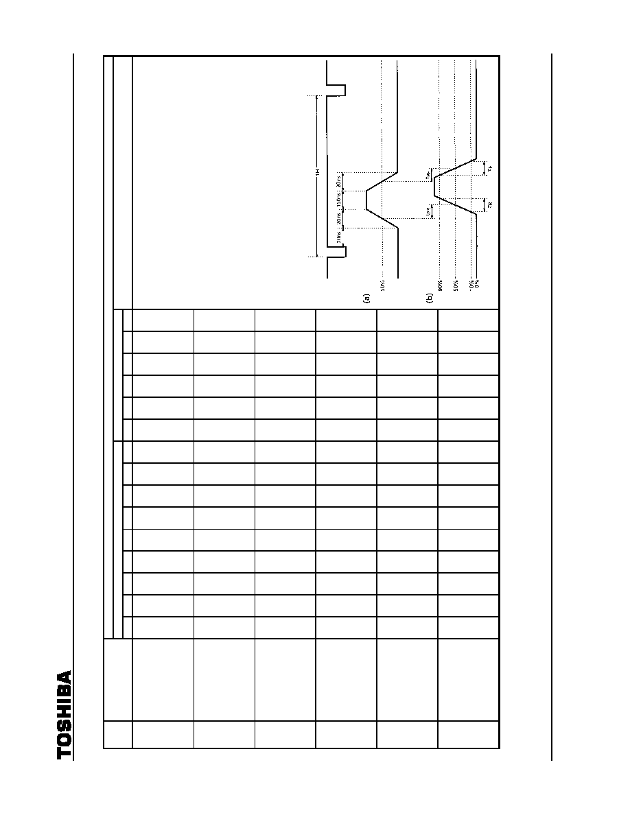
TB1227CNG
2004-05-24
80
TEST CONDITION (Unless otherwise specified : H, RGB V
CC
= 9V ; V
DD
, Fsc V
DD
, Y / C V
CC
= 5V ; Ta = 25±3∞C ; BUS = preset value)
SW MODE
SUB-ADDRESS & BUS DATA
NOTE ITEM
S
18
S
19
S
20
S
21
S
22
S
31
S
33
S
34
S
51
--
--
--
--
--
--
MEASURING METHOD
T
46
OSD Hi DC Switching
Rise-Up Time
A A A A B
B
B
B
A
--
--
--
--
-- --
T
47
OSD Hi DC Switching
Rise-Up Transfer
Time
--
--
--
--
--
--
T
48
OSD Hi DC Switching
Rise-Up Transfer
Time, 3 Axes
Difference
--
--
--
--
--
--
T
49
OSD Hi DC Switching
Breaking Time
--
--
--
--
--
--
T
50
OSD Hi DC Switching
Breaking Transfer
Time
--
--
--
--
--
--
T
51
OSD Hi DC Switching
Breaking Transfer
Time, 3 Axes
Difference
--
--
--
--
--
--
(1) Supply pin 21 (Digital Ys) with 2.5V.
(2) Input
5V
p-p
signal shown by (a) in the figure to pin 18 (Digital R IN).
(3) Referring to (b) of the following figure, measure
Rosh
, t
PRoh
,
Fosh
and t
PFoh
for output signal of pin 14 (R OUT).
(4) Input
5V
p-p
signal shown by (a) in the figure to pin 19 (Digital G
IN).
(5) Perform the same measurement as the above step 3 for pin 13
output (G OUT) referring to (b) of the following figure.
(6) Input 5Vp-p signal shown by (a) in the figure to pin 20 (Digital B
IN).
(7) Perform the same measurement as the above step 3 for pin 12
output (B OUT) referring to (b) of the following figure.
(8) Find maximum axes differences in t
PRoh
and t
PFoh
among the
three outputs (t
PRoh
, t
PFoh
).
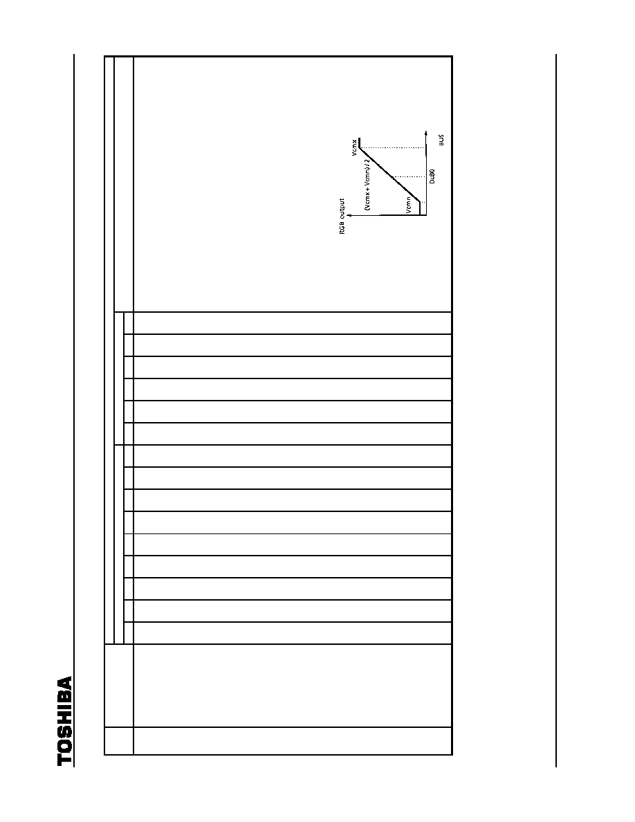
TB1227CNG
2004-05-24
81
TEST CONDITION (Unless otherwise specified : H, RGB V
CC
= 9V ; V
DD
, Fsc V
DD
, Y / C V
CC
= 5V ; Ta = 25±3∞C ; BUS = preset value)
SW MODE
SUB-ADDRESS & BUS DATA
NOTE ITEM
S
21
S
22
S
31
S
33
S
34
S
51
--
--
--
06H
--
--
--
-- --
MEASURING METHOD
T
52
RGB Contrast Control
Characteristic
B A B B B
A
--
--
--
FFH
80H
00H
--
--
--
--
--
(1) Input 0.3V synchronizing signal to pin 51 (Sync IN).
(2) Supply 5V of external supply voltage to pin 22 (Analog Ys).
(3) Set bus data on drive at center value.
(4) Input TG7 sine wave signal (f = 100kHz, video amplitude = 0.5V) to
pin 23 (Analog R IN).
(5) While changing data on RGB contrast from maximum (FF) to
minimum (00), measure maximum and minimum amplitudes of pin
14 (R OUT) in video period. At the same time, measure video
amplitude of pin 14 when the bus data is set at the center value
(80). (Vc14mx, Vc14mn, D14c80)
(6) In the same manner as the above steps 4 and 5, measure output
signal of pin 13 with input of the same external power supply to pin
24 (Analog G IN), and measure output signal of pin 12 with input of
the same power supply to pin 25 (Analog B IN). (Vc12mx, Vc12mn,
D12c80).
(7) Find amplitude ratio between signal with maximum unicolor data
and signal with minimum unicolor data in conversion into decibel
(V13ct).

TB1227CNG
2004-05-24
82
TEST CONDITION (Unless otherwise specified : H, RGB V
CC
= 9V ; V
DD
, Fsc V
DD
, Y / C V
CC
= 5V ; Ta = 25±3∞C ; BUS = preset value)
SW MODE
SUB-ADDRESS & BUS DATA
NOTE ITEM
S
21
S
22
S
31
S
33
S
34
S
51
--
--
--
06H
--
--
--
-- --
MEASURING METHOD
T
53
Analog RGB AC Gain
B
A
B
B
B
A
--
--
--
--
--
--
--
--
--
In the setting condition of the Note T
52
, calculate output / input gain
(double) with contrast data being set maximum.
G = Vc13mx / 0.5V
T
54
Analog RGB
Frequency
Characteristic
--
--
--
FFH
--
--
--
--
--
(1) Input 0.3V synchronizing signal to pin 51 (Sync IN).
(2) Supply 5V of external supply voltage to pin 22 (Analog Ys).
(3) Input TG7 sine wave signal (f = 100kHz, video amplitude = 0.5V) to
pin 24 (Analog G IN).
(4) Set bus data so that contrast is maximum and drive is set at center
value.
(5) Measure video amplitude of pin 13 (G OUT) and calculate output /
input gain (double) (G6M).
(6) From measurement results of the above step 5 and the preceding
Note 53, find frequency characteristic.
Gf
=
20og (G6M / G)

TB1227CNG
2004-05-24
83
TEST CONDITION (Unless otherwise specified : H, RGB V
CC
= 9V ; V
DD
, Fsc V
DD
, Y / C V
CC
= 5V ; Ta = 25±3∞C ; BUS = preset value)
SW MODE
SUB-ADDRESS & BUS DATA
NOTE ITEM
S
21
S
22
S
31
S
33
S
34
S
51
--
--
--
01H 06H
--
--
-- --
MEASURING METHOD
T
55
Analog RGB Dynamic
Range
B
A
B
B
B
A
--
--
--
--
00H
--
--
--
--
(1) Input 0.3V synchronizing signal to pin 51 (Sync IN).
(2) Supply 5V of external supply voltage to pin 22 (Analog Ys).
(3) Set bus data so that contrast is minimum and drive is set at center
value.
(4) While inputting stepping signal to pin 24 (Analog G IN), increase
video amplitude gradually from 0.
(5) Measure video amplitude of pin 24 when video voltage of pin 13
(G OUT) does not change.
T
56
RGB Brightness
Control Characteristic
--
--
--
FFH
00H
--
--
--
--
--
T
57
RGB Brightness
Center Voltage
--
--
--
80H
--
--
--
-- --
T
58
RGB Brightness Data
Sensitivity
--
--
--
--
--
--
--
--
--
(1) Short circuit pin 31 (Y IN), pin 33 (B-Y IN) and pin 34 (R-Y IN) in
AC coupling.
(2) Input 0.3V synchronizing signal to pin 51 (Sync IN).
(3) Set bus data on RGB cutoff at center value.
(4) Supply 5V of external supply voltage to pin 22 (Analog Ys).
(5) While changing data brightness from maximum to minimum,
measure maximum and minimum voltages of pin 13 (G OUT) in
video period. (max : Vbrmx, min : Vbrmn)
(6) Set bus data on brightness at center value and measure video
voltage of pin 13 (G OUT) (Vbcnt).
(7) On the condition that bus data with which Vbrmx is obtained in
measurement of the above step 5 is Dbrmx and bus data with
which Vbrmn is obtained in measurement of the above step 5 is
Dbrmn, calculate sensitivity of brightness data (Vbrt).
Vbrt = (Vbrmx - Vbrmn) / (Dbrmx - Dbrmn)
T
59
Analog RGB Mode
ON Voltage
--
--
--
80H
--
--
--
-- --
(1) Input TG7 sine wave signal (f = 100kHz, video amplitude = 0.3V) to
pin 23 (Analog R IN).
(2) Supply 5V of external supply voltage to pin 22 (Analog Ys) and
raise the voltage gradually from 0V.
(3) Measure voltage at pin 22 when signal 1 is output from pin 14 (R
OUT) (Vanath).

TB1227CNG
2004-05-24
84
TEST CONDITION (Unless otherwise specified : H, RGB V
CC
= 9V ; V
DD
, Fsc V
DD
, Y / C V
CC
= 5V ; Ta = 25±3∞C ; BUS = preset value)
SW MODE
SUB-ADDRESS & BUS DATA
NOTE ITEM
S
21
S
22
S
31
S
33
S
34
S
51
--
--
--
--
--
--
--
--
--
MEASURING METHOD
T
60
Analog RGB
Switching Rise-Up
Time
B
A
B
B
B
A
--
--
--
--
--
--
--
--
--
T
61
Analog RGB
Switching Rise-Up
Transfer Time
--
--
--
--
--
--
--
--
--
T
62
Analog RGB
Switching Rise-Up
Transfer Time, 3 Axes
Difference
--
--
--
--
--
--
--
--
--
T
63
Analog RGB
Switching Breaking
Time
--
--
--
--
--
--
--
--
--
T
64
Analog RGB
Switching Breaking
Transfer Time
--
--
--
--
--
--
--
--
--
T
65
Analog RGB
Switching Breaking
Transfer Time, 3 Axes
Difference
--
--
--
--
--
--
--
--
--
(1) Supply signal (2V
p-p
) shown by (a) in the following figure to pin 22
(Analog Ys).
(2) Referring to (b) of the following figure, measure
Rana
, t
PRan
,
Fana
and t
PFan
for outputs of pin 14 (R OUT), pin 13 (G OUT) and
pin 12 (B OUT).
(3) Find maximum values of t
PRan
and t
PFan
respectively
(t
PRan
, t
PFan
).

TB1227CNG
2004-05-24
85
TEST CONDITION (Unless otherwise specified : H, RGB V
CC
= 9V ; V
DD
, Fsc V
DD
, Y / C V
CC
= 5V ; Ta = 25±3∞C ; BUS = preset value)
SW MODE
SUB-ADDRESS & BUS DATA
NOTE ITEM
S
21
S
22
S
31
S
33
S
34
S
51
--
--
--
--
--
--
--
--
--
MEASURING METHOD
T
66
Analog RGB Hi
Switching Rise-Up
Time
B
A
B
B
B
A
--
--
--
--
--
--
--
--
--
T
67
Analog RGB Hi
Switching Rise-Up
Transfer Time
--
--
--
--
--
--
--
--
--
T
68
Analog RGB Hi
Switching Rise-Up
Transfer Time, 3 Axes
Difference
--
--
--
--
--
--
--
--
--
T
69
Analog RGB Hi
Switching Breaking
Time
--
--
--
--
--
--
--
--
--
T
70
Analog RGB Hi
Switching Breaking
Transfer Time
--
--
--
--
--
--
--
--
--
T
71
Analog RGB Hi
Switching Breaking
Transfer Time, 3 Axes
Difference
--
--
--
--
--
--
--
--
--
(1) Supply 2V to pin 22 (Analog Ys).
(2) Input
0.5V
p-p
signal shown by (a) in the following figure to pin 23
(Analog R IN).
(3) Referring to (b) of the following figure, measure
Ranh
, t
PRah
,
Fanh
and t
PFah
for output of pin 14 (R OUT).
(4) Input
0.5V
p-p
signal shown by (a) in the following figure to pin 24
(Analog G IN).
(5) Referring to (b) of the following figure, perform the same
measurement as the above step 3 for output of pin 13
(G OUT).
(6) Input
0.5V
p-p
signal shown by (a) in the following figure to pin 25
(Analog B IN).
(7) Referring to (b) of the following figure, perform the same
measurement as the above step 3 for output of pin 12
(B OUT).
(8) Find maximum axes difference in t
PRoh
and t
PFoh
among the three
outputs (t
PRah
, t
PFah
).

TB1227CNG
2004-05-24
86
TEST CONDITION (Unless otherwise specified : H, RGB V
CC
= 9V ; V
DD
, Fsc V
DD
, Y / C V
CC
= 5V ; Ta = 25±3∞C ; BUS = preset value)
SW MODE
SUB-ADDRESS & BUS DATA
NOTE ITEM
S
21
S
22
S
31
S
33
S
34
S
51
--
--
--
--
--
--
--
--
--
MEASURING METHOD
T
72
TV-Analog RGB
Crosstalk
B
A
B
B
B
A
--
--
--
--
--
--
--
--
--
(1) Input TG7 sine wave signal (f = 4MHz, video amplitude = 0.5V) to
pin 31 (Y
2
IN).
(2) Short circuit pin 25 (Analog G IN) in AC coupling.
(3) Input 0.3V synchronizing signal to pin 51 (Sync IN).
(4) Set bus data so that contrast is maximum, Y sub contrast and drive
are set at center value.
(5) Supply pin 22 (Analog Ys) with 0V of external power supply.
(6) Measure video voltage of output signal of pin 13 (G OUT) (Vtg).
(7) Supply pin 22 (Analog Ys) with 2V of external power supply.
(8) Measure video voltage of output signal of pin 13 (G OUT) (Vana).
(9) From measurement results of the above steps 5 and 7, calculate
crosstalk from TV to analog RGB.
Crtva
=
20og (Vana / Vtv)
T
73
Analog RGB-TV
Crosstalk
--
--
--
--
--
--
--
--
--
(1) Short circuit pin 31 (Y
2
IN), pin 34 (R-Y IN) and pin33 (B-Y IN) in
AC coupling.
(2) Input 0.3V synchronizing signal to pin 51 (Sync IN).
(3) Set bus data so that contrast is maximum and drive is set at center
value.
(4) Input TG7 sine wave signal (f = 4MHz, video amplitude = 0.5V) to
pin 24 (Analog G IN).
(5) Supply pin 22 (Analog Ys) with 0V of external power supply.
(6) Measure video voltage of output signal of pin 13 (G OUT) (Vant).
(7) Supply pin 22 (Analog Ys) with 2V of external power supply.
(8) Measure video voltage of output signal of pin 13 (G OUT) (Vtan).
(9) From measurement results of the above steps 6 and 8, calculate
crosstalk from analog RGB to TV.
Crant = 20og (Vant / Vtan)

TB1227CNG
2004-05-24
87
TEST CONDITION (Unless otherwise specified : H, RGB V
CC
= 9V ; V
DD
, Fsc V
DD
, Y / C V
CC
= 5V ; Ta = 25±3∞C ; BUS = preset value)
SW MODE
SUB-ADDRESS & BUS DATA
NOTE ITEM
S
21
S
22
S
31
S
33
S
34
S
51
--
--
--
01H 15H
--
--
-- --
MEASURING METHOD
T
74
ABL Point
Characteristic
B B B B B
A
--
--
--
FFH
10H
90H
F0H
--
--
--
--
(1) Input TG7 sine wave signal (f = 4MHz, video amplitude = 0.5V) to
pin 31 (Y
2
IN).
(2) Short circuit pin 23 (Analog R IN), pin 25 (Analog G IN) and pin 26
(Analog B IN) in AC coupling.
(3) Set bus data so that brightness is maximum and ABL gain is at
center value, and supply pin 16 with external supply voltage. While
turning down voltage supplied to pin 16 gradually from 7V,
measure voltage at pin16 when the voltage supplied to pin 12
decreases by 0.3V in three conditions that data on ABL point is set
at minimum, center and maximum values respectively. (Vablpl,
Vablpc, Vablph)
T
75
ACL
Characteristic
--
--
--
--
--
--
--
--
--
(1) Input TG7 sine wave signal (f = 4MHz, video amplitude = 0.5V) to
pin 31 (Y
2
IN).
(2) Input 0.3V synchronizing signal to pin 51 (Sync IN).
(3) Measure video amplitude at pin 12. (Vacl1)
(4) Measure DC voltage at pin 16 (ABCL).
(5) Supply pin 16 with a voltage that the voltage measured in the
above step 4 minus 2V.
(6) Measure video amplitude at pin 12 (Vacl2) and its ratio to the
amplitude measured in the above step 3.
Vacl = 20og (Vacl2 / Vacl1)
T
76
ABL Gain
Characteristic
--
--
--
FFH
00H
10H
1CH
--
--
--
--
(1) Short circuit pin 31 (Y
2
IN), pin 34 (R-Y IN) and pin 33 (B-Y IN) in
AC coupling.
(2) Input 0.3V synchronizing signal to pin 51 (Sync IN).
(3) Set bus data on brightness at maximum and measure video DC
voltage at pin 12 (Vmax).
(4) Measure voltage at pin 16 which is being supplied with the voltage
measured in the step 5 of the preceding Note 75.
(5) Changing setting of bus data on ABL gain at minimum, center and
maximum values one after another, measure video DC voltage at
pin 12. (Vabl1, Vabl2, Vabl3)
(6) Find respective differences of Vabl1, Vabl2 and Vabl3 from the
voltage measured in the above step 3.
Vabll = Vmax - Vabl1
Vablc
=
Vmax
- Vabl2
Vablh
=
Vmax
- Vabl3

TB1227CNG
2004-05-24
88
SECAM SECTION
TEST CONDITION (Unless otherwise specified : H, RGB V
CC
= 9V ; V
DD
, Fsc V
DD
, Y / C V
CC
= 5V ; Ta = 25±3∞C)
BUS : TEST MODE
BUS : NORMAL CONTROL MODE
S
02H 07H
0FH
10H
1FH
NOTE ITEM
26 D
4
D
3
D
2
D
7
D
5
D
4
D
4
D
7
D
5
D
4
D
3
D
2
D
1
D
0
D
7
D
6
D
5
D
4
D
3
D
2
D
1
D
0
MEASURING METHOD
S
1
Bell Monitor Output
Amplitude
ON 0 1 0 0 0
0
1
0
0
0
0
0
0
0
1
0
0 0 0 0
0
1
(1) Input
200mV
p-p
(R-Y ID), 75% chroma color
bar signal (SECAM system) to pin 42.
(2) Measure amplitude of R-Y ID output of pin 36
as ebmo.
S
2
Bell Filter f
o
(1) While supplying 20mV
p-p
CW sweep signal
from network analyzer to pin 42 and monitoring
output signal of pin 36 with the network
analyzer, measure frequency having maximum
gain as foBEL of the bell frequency
characteristic.
(2) Find difference between foBEL and 4.286MHz
as foB-C.
S
3
Bell Filter f
o
Variable
Range
Vari-
able
Vari-
able
(1) The same procedure as the steps 1 and 2 of
the Note S
2
.
(2) Measure foBEL in different condition that SUB
(IF) D
1
D
0
= (00) or (11), and find difference of
each measurement result from 4.286MHz as
foB-L or foB-H.
S
4
Bell Filter Q
0
1
(1) The same procedure as the step 1 of the Note
S
2
.
(2) While monitoring output signal of pin 36 with
network analyzer, measure Q of bell frequency
characteristic as QBEL.
QBEL = (QMAX -3dB band width) / FoBEL
S
5
Color Difference
Output Amplitude
OFF -- -- -- -- -- --
0
S
6
Color Difference
Relative Amplitude
-- -- -- -- -- --
(1) Input
200mV
p-p
(R-Y ID), 75% chroma color
bar signal (SECAM system) to pin 42.
(2) Measure color difference levels VRS and VBS
with signals of pin 35 and pin 36.
(3) Calculate relative amplitude from VRS / VBS.

TB1227CNG
2004-05-24
89
TEST CONDITION (Unless otherwise specified : H, RGB V
CC
= 9V ; V
DD
, Fsc V
DD
, Y / C V
CC
= 5V ; Ta = 25±3∞C)
BUS : TEST MODE
BUS : NORMAL CONTROL MODE
S
02H 07H
0FH
10H
1FH
NOTE ITEM
26 D
4
D
3
D
2
D
7
D
5
D
4
D
4
D
7
D
5
D
4
D
3
D
2
D
1
D
0
D
7
D
6
D
5
D
4
D
3
D
2
D
1
D
0
MEASURING METHOD
S
7
Color Difference
Attenuation Quantity
OFF --
--
--
--
-- --
0
0
0
0
0
0
0
0
1
1
0
0
0
0
0
1
(1) The same procedure as the steps 1 and 2 of the
Note S
5
.
(2) In the condition that SUB (IF) D
6
= 1, measure
amplitudes of color difference signals of pin 35
and pin36 as VRSA and VBSA respectively, and
find SATTR and SATTB from measurement
results.
SATTR
=
20og (VRSA / VRS),
SATTB = 20og (VBSA / VBS)
S
8
Color Difference S / N
Ratio
-- -- -- -- -- --
0
(1) The same procedure as the steps 1 and 2 of the
Note S
5
.
(2) Input
non-modulated
200V
p-p
(R-Y) chroma
signal to pin 42.
(3) Measure noise amplitude nR and nB (mV
p-p
)
appearing in color difference signals of pin 35 and
pin 36 respectively.
(4) Find S / N ratio by the following equation.
3)
10E
nB
/
VBS
2
(2
og
20
S
-
SNB
-
◊
◊
=
l
3)
10E
nR
/
VRS
2
(2
og
20
S
-
SNR
-
◊
◊
=
l
S
9
Linearity
-- -- -- -- -- --
(1) The same procedure as the step 1 of the Note S
5
.
(2) Measure and calculate amplitude of black bar
levels in output waveforms of pin 35 and pin 36 as
shown below.
LinB = V [cyan] / V [red]
LinR = V [yellow] / V [blue]
Maximum positive /
negative amplitudes in
respective axes

TB1227CNG
2004-05-24
90
TEST CONDITION (Unless otherwise specified : H, RGB V
CC
= 9V ; V
DD
, Fsc V
DD
, Y / C V
CC
= 5V ; Ta = 25±3∞C)
BUS : TEST MODE
BUS : NORMAL CONTROL MODE
S
02H 07H
0FH
10H
1FH
NOTE ITEM
26 D
4
D
3
D
2
D
7
D
5
D
4
D
4
D
7
D
5
D
4
D
3
D
2
D
1
D
0
D
7
D
6
D
5
D
4
D
3
D
2
D
1
D
0
MEASURING METHOD
S
10
Rising-Fall Time
(Standard
De-Emphasis)
OFF -- -- -- -- --
--
0
0
0
0
0
0
0
0
1
0
0 0 0 0
0
1
S
11
Rising-Fall Time
(Wide-Band
De-Emphasis)
--
--
--
--
--
--
(1) The same procedure as the step 1 of the Note S
5
.
(2) Measure output waveforms of pin 35 and pin 36
to find the period between the two points shown in
the figure in time.
(3) In the condition that SUB (IF) D
5
= 1, perform the
same measurement as the above step 2.
Measurement results are expressed as t
rfBW
and
t
rfRW
.
S
12
Killer Operation Input
Level (Standard
Setting)
--
--
--
--
--
--
1
S
13
Killer Operation Input
Level (VID ON)
--
--
--
--
--
--
0
1
S
14
Killer Operation Input
Level (Low Sensitivity,
VID OFF)
--
--
--
--
--
--
0 1
(1) Input
200mV
p-p
(R-Y ID) standard 75% color bar
signal (SECAM system) to pin 42.
(2) Attenuate the input signal to pin 42. Measure R-Y
ID signal level at pin 42 that turns on / off the killer
as eSK and eSC.
(3) In the condition that SUB (IF) D
3
= 1, perform the
same measurement as the above step 2 and
express the measurement results as eSFK and
eSFC.
(4) In the condition that SUB (IF) D
3
= 0, D
2
= 1,
perform the same measurement as the above
step 2 and express the measurement results as
eSWK and eSWC.

TB1227CNG
2004-05-24
91
TEST CIRCUIT
T B 1 2 2 7 C N G

TB1227CNG
2004-05-24
92
APPLICATION CIRCUIT
T B 1 2 2 7 C N G

TB1227CNG
2004-05-24
93
PACKAGE DIMENSIONS
Weight: 5.55g (Typ.)

TB1227CNG
2004-05-24
94
∑ The information contained herein is subject to change without notice.
∑ The information contained herein is presented only as a guide for the applications of our products. No
responsibility is assumed by TOSHIBA for any infringements of patents or other rights of the third parties which
may result from its use. No license is granted by implication or otherwise under any patent or patent rights of
TOSHIBA or others.
∑ TOSHIBA is continually working to improve the quality and reliability of its products. Nevertheless, semiconductor
devices in general can malfunction or fail due to their inherent electrical sensitivity and vulnerability to physical
stress. It is the responsibility of the buyer, when utilizing TOSHIBA products, to comply with the standards of
safety in making a safe design for the entire system, and to avoid situations in which a malfunction or failure of
such TOSHIBA products could cause loss of human life, bodily injury or damage to property.
In developing your designs, please ensure that TOSHIBA products are used within specified operating ranges as
set forth in the most recent TOSHIBA products specifications. Also, please keep in mind the precautions and
conditions set forth in the "Handling Guide for Semiconductor Devices," or "TOSHIBA Semiconductor Reliability
Handbook" etc..
∑ The TOSHIBA products listed in this document are intended for usage in general electronics applications
(computer, personal equipment, office equipment, measuring equipment, industrial robotics, domestic appliances,
etc.). These TOSHIBA products are neither intended nor warranted for usage in equipment that requires
extraordinarily high quality and/or reliability or a malfunction or failure of which may cause loss of human life or
bodily injury ("Unintended Usage"). Unintended Usage include atomic energy control instruments, airplane or
spaceship instruments, transportation instruments, traffic signal instruments, combustion control instruments,
medical instruments, all types of safety devices, etc.. Unintended Usage of TOSHIBA products listed in this
document shall be made at the customer's own risk.
∑ The products described in this document are subject to the foreign exchange and foreign trade laws.
∑ TOSHIBA products should not be embedded to the downstream products which are prohibited to be produced
and sold, under any law and regulations.
030619EBA
RESTRICTIONS ON PRODUCT USE
About solderability, following conditions were confirmed
∑ Solderability
(1) Use of Sn-63Pb solder Bath
∑ solder bath temperature = 230∞C
∑ dipping time = 5 seconds
∑ the number of times = once
∑ use of R-type flux
(2) Use of Sn-3.0Ag-0.5Cu solder Bath
∑ solder bath temperature = 245∞C
∑ dipping time = 5 seconds
∑ the number of times = once
∑ use of R-type flux