 | –≠–ª–µ–∫—Ç—Ä–æ–Ω–Ω—ã–π –∫–æ–º–ø–æ–Ω–µ–Ω—Ç: TB1254N | –°–∫–∞—á–∞—Ç—å:  PDF PDF  ZIP ZIP |

�
Ver3.7
00/01/28
1
TENTATIVE TOSHIBA Bi-CMOS INTEGRATED CIRCUIT, SILICON MONOLITHIC
TB1254N
PAL / NTSC / SECAM 1CHIP (IF+VCD PROCESSOR) IC
The TB1254N is a TV signal processor IC, which contains
PIF, SIF, Video, Chroma and deflection signal processors
for worldwide Multi-color systems. Also, it has AV switch
for TV/EXT inputs.
The line-up and flexibility of this TB1251 series contributes
to reduce development costs and components in a TV
sets.
FEATURES
IF STAGE
Multi-system IF
SIF 4.5 ~ 6.5 MHz
One External BPF for Multi-SIF carrier
Inter carrier inputs
VCO tank coil alignment free
for
L
system,
Positive demodulation
V low Ch
VIDEO STAGE
Built-in Y delay line (8 adjustable steps)
Built in C trap filter (Switchable)
CHROMA STAGE
Multi-color
Demoduration
Automatic
Chroma
Identification
1 Xtal for Multi-color Systems
(3.58MHz/4.43MHz/M-PAL/N-PAL)
Built-in1H Delay line
Cb/Cr input ports
Built-in BPF / TOF
Fsc
Output
Two NTSC demodulation phase
SDIP56-P-600
TEXT STAGE
Built-in
AKB
AKB on/off
AKB Color temperature control
Analog RGB interfaces
ABL / ACL
DEFLECTION STAGE
Built-in
H-VCO
ramp distortion correction
Stand Along Sync in port
Sand Castle Pulse Output
(HD+VD+Gate Pulse)
AV SWITCH
Visual TV / EXT inputs
Audio TV / EXT inputs
TOSHIBA is continually working to improve the quality and the reliability of its products. Nevertheless,
semiconductor devices in general can malfunction or jail due to their inherent electrical sensitivity and
vulnerability to physical stress. It is the responsibility of the buyer, when utilizing TOSHIBA products, to
observe standards of safety, and to avoid situations in which a malfunction or failure of a TOSHIBA product could
cause loss of human life, bodily injury or damage to property. In developing your designs, please ensure that
TOSHIBA products are used within specified operating range as set forth in the most recent products specifications.
Also, please keep in mind the precautions and conditions set forth in the TOSHIBA Semiconductor Reliability
Handbook.
The products described in this document are subject to foreign exchange and foreign trade control laws.
The information contained herein is presented only as a guide for the applications of our products. No
responsibility is assumed by TOSHIBA CORPORATION for any infringements of intellectual property or other rights of
th
thi d
ti
hi h
lt
f
it
N
li
i
t d
b
i
li
ti
th
i
d
Weight: 5.55g (typ)

�
Ver3.7
00/01/28
2
56
50
51
52
53
54
55
49
43
44
45
46
47
48
42
36
37
38
39
40
41
35
29
30
31
32
33
34
1
7
6
5
4
3
2
8
14
13
12
11
10
9
15
21
20
19
18
17
16
22
28
27
26
25
24
23
SDA
SCL
Sync in
I2C Bus
IF
Cutoff/Drive
<R.G.B.CUTTOFF>
<R.G.B.DRIVE>
<AKB SW>
<AKB W/B controle>
Matrix / SW
RGB Interface
Bright <RGB BRT>
Uni-Color<RGB CONT>
Mode SW
EW PROC.
<H.SIZE>
<EW PARA.>
<TRAPEZIUM>
<EW CONER>
TB1254N BLOCK DIAGRAM
EHT H/V
<EHT.H>
<EHT.V>
Y IN
V PROC.
<V.SIZE>
<V.LINEAR.>
<V-S CORR.>
<V.SHIFT>
FM DEMOD.
Gain Sw
AUDIO ATT
<ATT>
Chroma DEMOD.
PAL/NTSC/SECAM
1H delay line
1 X'tal
<TINT>
<color system>
<F ID>
<Killer Sence>
PIF Proc.
L-SECAM
DEF Proc.
H,V synchronization
<Lock det.>
<Sync det>
<AFC1 Gain>
Chroma Baseband Proc.
<Color>
<Unicolor>
Clamp
BBTINT
6dB
IF IN
SAW
IF GND
Ripple F
IF AGC
+
APC Filter
+
4.43MHz X'tal
CW OUT
Ys/Ym
EXT.R IN
EXT.G IN
EXT.B IN
RGB Vcc(9V)
+
R OUT
G OUT
B OUT
IK IN
V RAMP
V NFB
V OUT
EXT AUDIO IN
DC NF
+
EXT IN
C in
BLACK Det
+
Cb in
DC Restor
ABCL IN
YC Vcc(5V)
+
Dig GND
YC GND
H OUT
H Vcc(9V)
H.AFC
FBP IN/SCP OUT
DE-EMP.
Dig.VDD
+
+
TV in
IF DET OUT
Hcorr IN/SIF IN
PIF tank
+
6.5MHz
,a,o,e
TRAP
Y Proc.
Clamp
C-TRAP
<c-trap>
Black Stretch
<B.S.>
DC restore
<DC rest>
Y-¡
<¡>
Y-D.L.
<DL>
A.C.
<P.SHARP>
Sub-Cont
<S.CONT>
Uni-Color
<CONT>
Bright
<BRT>
WPS
Half T.
<H.T>
<ABL START P>
<ABL GAIN>
IF Vcc(5V)
+
LOOP Filter
+
SIF OUT
AUDIO OUT
AFT OUT
MONITOR OUT
Cr in
ref R
SIF
Processor
6.5MHz
Uni-SIF beet up
RF AGC
+
N.C.
BIAS

�
Ver3.7
00/01/28
3
TERMINAL INTERFACE
PIN NAME
FUNCTION
INTERFACE
1
IF VCC
A Vcc terminal for the IF circuit.
Supply 5V.
∑
2
RIPPLE
FILTER
A terminal to be leaded to an internal bias
filter. Put a capacitor.
2
5
1
330∂
330∂
27.5k∂
45k∂
2k∂
1k∂
3
SIF OUT
An output terminal for a 1st SIF signal, that
beaten down by a regenerated carrier.
The SIF frequencies are able to convert into
only 6.5MHz, in order to eliminate SIF BPFs
to single 6.5MHz.
3
5
14
100∂
500∂
15k∂
9V
16.3k∂
16k∂
4
AUDIO OUT
An output terminal for audio signal.
FM Det.signal or the external audio signal,
input to pin53, is output (Switched by bus).
An internal audio attenator controles the
output levelS.
∑
4
5
14
50k∂
5.3V
ATT
9V
30k∂
100∂
5
IF GND
The GND terminal for IF circuit.
∑
6
7
IF IN
IF IN
Input terminals for IF signals. Pin 6 and 7 are
the both input poles of a differential amplifier.
The norminal input level is 90dB(
∑
V)(Pin6-7),
input impedance is 1.5 k ohms.
6
5
1
7
100k∂
1.44k∂
1.44k∂
1.5V
2.75V
8
NC
-

�
Ver3.7
00/01/28
4
PIN NAME
FUNCTION
INTERFACE
9
RF AGC
An output terminal for RF AGC.
A pull up resister is required because of its
open collector output, and also connect de-
coupling capacitor to reduce noises,.
9
5
14
9V
300∂
30k∂
30k∂
to SELF ADJ
10
IF AGC
A terminal to be connected to an IF AGC
filter. Connect 2.2
∑
F of capacitor to Vcc
10
5
1
2k∂
11
APC FILTER
A terminal to be connected with an APC filter
for chroma demodulation.
This terminal voltage controls the frequency
of VCXO.
11
19
42
220∂
110k∂
3.2V
12
X'TAL
(4.43MHZ)
A terminal to be connected with a
4.433619MHz X'tal oscillator. The oscillated
signal lead to chroma demodulation, H out
frequency tuning, AFT and so on.
12
19
42
500 ∂
2.5k ∂
13
CW OUT
An output terminal for the continuous chroma
sub-carrier frequency wave, which amplitude
is 0.7Vp-p (typ).
Also the dc level shows killer status, the level
is 1.5V for B/W and 3.5V for Color.
13
19
42
200∂
1k∂

�
Ver3.7
00/01/28
5
PIN NAME
FUNCTION
INTERFACE
14
RGB VCC (9V)
A Vcc terminal for RGB block, PIF det. Output
and sound output circuit.
Supply 9V.
∑
15
YS/YM SW
∑
Spot killer
A terminal for switching of EXT RGB Mode
and fast Half tone.
15
14
42
3.3V
250∂
0.7V
16
17
18
EXT. R IN
EXT. G IN
EXT. B IN
Input terminals for EXT RGB signals. The
signals are clamped by capacitors, therefore
the input impedance should be low, 100
ohms or less is recommended.
For this input, brightness and RGB contrast
are available, also ABL/ACL eliminate the
output leval. This ABL/ACL is able to off.
OFF: for small area like OSD
ON: for large area like TELETEXT
(input level 0.7Vp-p/100IRE)
16
19
42
250∂
250∂
2.3V
17
18
250∂
250∂
100uA
19
Y/C GND
The GND terminal for Y/C circuit.
∑
20
21
22
R OUT
G OUT
B OUT
Terminals for R/G/B signal output.
Connect resistances to GND, if through rate
is not enough. Because of source current
limitation, the resistances should be 2.0k
∑
or
more.
20
19
14
100∂
21
22
23
IK IN
An input terminal to sense AKB cathode
current.
Connect this terminals to GND if not using
the AKB system.
23
19
42
2.5k∂
2.5k∂
5k∂
2.5k∂
25k∂
50k∂
12.5k∂
1k∂
VF
VK
1k∂
soft
start
limitter
over circuit

�
Ver3.7
00/01/28
6
PIN NAME
FUNCTION
INTERFACE
24
V RAMP
A terminal to be connected with a capacitor to
generate the V.Ramp signal.
The V.Ramp amplitude is kept constant by
the V.AGC.
24
33
31
2.7k∂
V AGC
200∂
25
V
NFB
An input terminal for V saw-teeth signal
feedback.
If the DC voltage on this pin is less than 1.7V,
it blanks RGB output for V guard.
12.5k∂
25
33
31
2V
V GUARD
26
V OUT
An output terminal for the vertical driving
pulses.
26
33
31
200∂
30k∂
1k∂
V OUT read
0.5V
27
REF. R
A terminal to be connected with resistance to
stabilize internal current sources.
Connect 5.6 k
1% of resistance to GND.
27
33
1.12V
31
6.8k
49k

�
Ver3.7
00/01/28
7
PIN NAME
FUNCTION
INTERFACE
28
ABCL IN
An input terminal for ABL/ACL control.
Control voltage range is 5.5
∑
6.0V.
The ratio of ABL against ACL can be set by
bus control.
29
H AFC FILTER
A terminal to be connected with H. AFC Filter.
The DC voltage of this pin controls the H
VCO frequency.
29
33
31
100k∂
50∂
237∂
75k∂
30
FBP IN/ SCP
OUT
An input terminal for FBP.
The V and GP Pulses are overlaid as SCP.
protect
GP
VD
H AFC
H BLK
30
33
31
3VF
VD
1.4V
3.5V
GP
31
H VCC (9V)
A Vcc terminal for DEF circuit, HOUT,
IICBUS POR etc.
Supply 9V.
∑
32
H OUT
An output terminal for horizontal driving
pulses.
32
33
31
2VF
6k∂
50∂
33
DIG GND
A GND terminal for digital block.
∑

�
Ver3.7
00/01/28
8
PIN NAME
FUNCTION
INTERFACE
34
SCL
An input terminal for IICBUS clock.
34
5k∂
3.25V
31
33
35
SDA
An input/output terminal for IICBUS data.
35
5k∂
3.25V
31
33
36
BLACK DET
A terminal to be connected with Black det.
filter for black stretch.
This terminal voltage controls Black
stretching gain.
The IIC Bus controls on/off and start point of
Black stretch.
36
2.5V
19
42
4k∂
37
DIG. VDD
A Vdd terminal for of digital block.
Supply HVcc voltage through 270 ohms of
resistance.
The voltage of this terminal is clipped in
about 3.3V by the internal regulator.
2.6V
30∂
30∂
750∂
37
VDD
31
H VCC
30∂

�
Ver3.7
00/01/28
9
PIN NAME
FUNCTION
INTERFACE
38
SYNC IN
An input terminal for Sync signal.
The input sync chip is clamped by
charging/discharging the coupling capacitors
so as to align the Sync slice level, therefore
input through low impedance buffer.
(input level 1Vp-p/140IRE)
38
33
31
1k∂
6k∂
24k∂
832∂
3VF
39
Y IN
An input terminal for Y signal.
The pedestal level is clamped by means of
charging/discharging the coupling capacitor,
therefore input through low impedance buffer.
(1Vp-p/140IRE input level)
39
1k∂
1k∂
1k∂
<Amp>
<Clamp> <read Bus>
42
19
40
DC RESTOR
A terminal to be connected with a capacitor to
detect the average picture level for DC
restoration.
The ratio of the DC restoration is set by bus.
Leave this terminal open if the DC restoration
is not required.
40
19
42
10k
50k
41
MON OUT
An output terminal of AV SW monitor.
The input signal for pin # 46/48 is output
through 6dB amplifier .
(output level 2Vp-p/140IRE)
41
19
14
8k∂
8k∂
2V
42
Y/C VCC
An Vcc terminal for Y/C circuit.
Supply 5V.
∑

�
Ver3.7
00/01/28
10
PIN NAME
FUNCTION
INTERFACE
43
C-IN
An input terminal for chroma signal.
(standard burst amplitude level 286mVp-p
∑
The low/High impedance status of this pin
can be read by bus to detect if S port is
connected or not.
43
19
42
75k∂
2.25V
1k∂
44
45
Cr IN
Cb IN
Input terminals for Cb/Cr signals.
This terminal is clamped by charging /
discharging the coupling capacitors, therefore
input with low impedance, 100
∑
or less are
recommended.
B.B.TINT
∑
-/+12deg
∑
Sub color control are
available for Cb/Cr input signals.
44
19
42
clamp
2.5V
45
46
EXT IN
An input terminal for external video signal.
(input level 1Vp-p / 140 IRE)
46
19
14
2V
1k∂
200∂
1k∂
47
LOOP FILTER
A terminal to be connected with loop filter for
PIF PLL.
The terminal voltage is controlled PIF VCO
frequency.
47
5
1
500∂
5V
1k∂
1k∂
15k∂

�
Ver3.7
00/01/28
11
PIN NAME
FUNCTION
INTERFACE
48
TV IN
An input terminal for TV video signal.
(input level 1Vp-p / 140 IRE)
48
19
14
2V
1k∂
200∂
1k∂
49
De-Emphasis
∑
Mon-OUT
A terminal to De-Emphasis Audio signal, and
pick up detected Audio signal. Connect
capacitor (0.01
∑
F to GND.
The time constant 50/75us is set by the
IICBUS control "SIF Freq".
Remove the capacitor in case of use US/JPN
sound multiplex system.
49
5
14
15k∂ 7.5k∂ 500∂
50
51
PIF TANK
Terminals to connect a PIF tank coil.
The tank coil should be pre-set up within +/-
2% for the automatic tuning. Manual tuning is
also available..
The resonance capacitance of the tank
should be 18pF.
50
5
1
51
52
DC NF
A terminal for connect the capacitor for DC
NF.
52
5
14
2k∂ 10k∂

�
Ver3.7
00/01/28
12
PIN NAME
FUNCTION
INTERFACE
53
EXT AUDIO IN
An input terminal for external audio signal.
Nominal input level is 500mVrms.
53
19
14
4.5V
35k
35k
54
IF DET OUT
An output terminal of detected PIF.
(typical output level 2.2Vp-p)
54
200∂
1k∂
5
14
55
AFT OUT
An output terminal for AFT.
output dc range;
0
∑
2.5
∑
5V.
output impedance; 50 k ohms (typ.)
55
5
1
100k∂
100∂
100k∂
3.4V
1.7V
AFT OUT
AFT READ
SELF TEST
OUT
56
SIF in / H corr.
An input terminal for 2'nd SIF signal and
H.curve correction.
56
1
5
20k∂
7pF
2.5V
500
SIF
H corr

�
Ver3.7
00/01/28
13
BUS CONTROL MAP for TB1254N
Write Mode
Slave Address: 88 HEX
Sub
Addr.
D7
MSB
D6
D5
D4
D3
D2
D1
D0
LSB
PRESET
00
WPS
Uni-Color
0000 0000
01
B.B.
Brightness ( TV / Text )
0100 0000
02
C-Trap
Color
0100 0000
03
N Phase
Sharpness
0010 0000
04
Y MUTE
RGB Mt
RGB Contrast
0110 0000
05
Y D.L.
Sub Color
0011 0000
06
Video SW
Au SW
B.B.Tint
0001 0000
07
N-Comb
TINT
0100 0000
08
SECAM R-Y Black Adjust
SECAM B-Y Black Adjust
1000 1000
09
S- GP Phase
/ S- inhibit
S-ID Sens
Bell fo
S-Black
Monitor
L-SECAM
Mode
L-S AGC
Speed-up
S-ID
Mode
0000 0000
0A
PIF Freq
SIF Freq.
Color System
0000 0000
0B
6.5MHz
SIF Fix
Audio Att
0000 0000
0C
BPF/TOF
P/N-
ID Sens
F ID
Coring
off
SIF
5.74MHz
PIF VCO
Adj. Stop
PIF VCO
Adj. Req
PIF VCO
Center
0000 0000
0D
Sprit/
∑
nt
∑
∑
Over Mod
SW
Q Det
Gain
AFT Sens
Au Gain
AFT Mute
STD by Mode
0000 0000
0E
Self Test
RF AGC
0000 0000
0F
Ysm M
RGB
ABCL
DC Restoration
Black Stretch
Point
0000 0000
10
ABL Start Point
ABL Gain
Sub Contrast
0000 1000
11
AKB System
Buzz
reducer
color -
0001 1000
12
R Cut Off
0000 0000
13
G Cut Off
0000 0000
14
B Cut Off
0000 0000
15
Cb/Cr SW
G Drive Gain
0100 0000
16
BLK
B Drive Gain
0100 0000
17
H-Stop
V-Stop
V AGC
V Ramp
Ref.
V-Freq.
312/313
Mode
0000 0000
18
Vertical Position
Horizontal Position
0001 0000
19
V Linaerity
V S Correction
1000 1000
1A
AFC G
Vertical Size
0010 0000
1B
test(0)
test(0)
Horizontal Size
0010 0000
1C
*
*
EW Parabola correction
0010 0000
1D
EW Trapezium Correction
V. EHT
1000 0100
1E
VSM SW
EW Corner Correction
H. EHT
0100 0100
1F
Test Mode
0000 0000
READ Mode
7
6
5
4
3
2
1
0
R0
POR
IF Lock
H Lock
IF Level
V Freq
Color System
R1
Y-IN
RGB
OUT
H-OUT
V-OUT
PIF VCO
Adj.
V Lock
AFT
R2
Coil error
PIF- VCO
error det
SYNC
DET
C IN DC
Product Code
R3
AKB
Overflow
CRT
Warm up
AKB
finish
STD/Non
-STD
P ID
N-ID
S ID
noise
det

�
Ver3.7
00/01/28
14
IIC BUS CONROL FUNCTION
WRITE MODE
PIF STAGE
ITEMS
BITS
DESCRIPTIONS
PRESET
RF AGC
∑∑
Sub; 0E h
6
RF AGC delay point (Pin6-7)
01: 65 dB(
∑
V)
3F: 100 dB(
∑
V)
00: IF MUTE Stops Demodulation
00000
:Mute
IF Freq.
∑∑
Sub; 0A h
3
Setting IF frequency for digital AFT count down
000: 58.75 MHz
001: 45.75 MHz
010: 39.5 MHz
011: 38.9 MHz
100: 38.0 MHz
101: 34.47 MHz
110: 33.95 MHz
111: 34.2 MHz
000
:58.75MHz
AFT Mute
∑∑
Sub; 0D h
1
AFT Mute Switch
0: normal
1: AFT defeat (mute)
0:normal
AFT sens.
∑∑
Sub; 0D h
1
AFT sensitivity
0: 100kHz/v
1: 25kHz/V
0:100kHz
Over mod SW
∑∑
Sub; 0D h
1
on/off the over modulation switch
0: off
1: on
0:off
Q det. Gain
∑∑
Sub; 0D h
Q detector gain
0: high
1: low
0:high
L-SECAM Mode
∑∑
Sub; 09 h
1
L SECAM
0: Not L-SECAM
1: L-SECAM
turn the polarity for TV Det Out
∑
for positive modulation
∑
Delay the AGC time constant (Peek AGC)
SIF AM demodulation
0:Not
L-SECAM
L-SECAM AGC
Speed
∑∑
Sub; 09 h
1
Speed up the AGC sense for channel serch
0: normal
1: speed-up
∑
Ch Serch
∑
0:normal
VCO Center
∑∑
Sub; 0C h
1
VCO center SW
0: normal
1: Center
In adjusting a tank coil, set this bit to 1.
0: normal
VCO Adj. Request
∑∑
Sub; 0C h
1
VCO adjust trigger
0: normal
1: VCO adjust trigger
The PIF VCO starts adjusting after requested.
While adjusting, the picture is blanked
0: normal
VCO Adj. Stop
∑∑
Sub; 0C h
1
Stop the readjustment on detecting the loosing adjustment
0: normal
1: stop self adjustment
"VCO Adj request" prier it
0: normal
SIF STAGE
ITEMS
BITS
DESCRIPTIONS
PRESET
SIF Freq.
∑∑
Sub; 0A h
2
SIF Frequency
00: 5.5MHz
01: 6.0MHz
10: 6.5MHz
11: 4.5MHz
Set the SIF frequency for;
Select the SIF FM demodulator band
select the de-emphasis speed
Set the ref.freq. for single
∑∑∑
MHz beet up if using
00:5.5MHz
SIF 574
∑∑
Sub; 0C h
1
Set the SIF freq. to 5.74MHz for IGR Bilingual.
It sets the reference freq. for beet up the 5.74MHz to 6.5MHz.
0: other frequencies
1: 5.74MHz
0:other
frequencies

�
Ver3.7
00/01/28
15
ITEMS
BITS
DESCRIPTIONS
PRESET
Audio ATT
∑∑
Sub; 0B h
7
Audio attenuator
00: Mute 01: -85 dB ~ 7F: 0 dB
00: Mute
Au Gain
∑∑
Sub; 0D h
1
Audio Gain Switch
0:
927mVrms at 25kHz/DEV
1:
500mVrms at 25kHz/DEV
0:
927mVrms
at
25kHz/DEV
6.5MHz SIF Fix
∑∑
Sub; 0A h
1
Beet up the SIF carrier frequency to 6.5MHz (single carrier)
0: normal
1: beet up to uni- 6.5MHz
0: normal
Buzz Reducer
∑∑
Sub; 11 h
1
Nyquist Buzz Reducer SW
0: on
1: off
0: on
VIDEO STAGE
ITEMS
BITS
DESCRIPTIONS
PRESET
Sharpness
∑∑
Sub; 03 h
6
Sharpness control peak:2.75MHz
00: -5.4dB ~ 20: 3.3dB ~ 3F: 6.6 dB
00:-5.4dB
DC Rest.
∑∑
Sub; 0F h
2
DC Restoration control
00: 120%
01: 90%
10: 100%
11: 110%
00:120%
Black Stretch
∑∑
Sub; 0F h
2
Set the black stretch start point
00: off
01: 25IRE
10: 35IRE
11: 45IRE
00: off
∑
point
∑∑
Sub; 0F h
2
Set the non linear
curve for Y signal
00: off
01: 90IRE
10: 80IRE
11: 70IRE
00: off
Y DL
∑∑
Sub; 05 h
3
Y Delay time
000: -40ns
100: +120ns
001: 0ns
101: +160ns
010: +40ns
110: +200ns
011: +80ns
111: +240ns
001: 0ns
C-Trap
∑∑
Sub; 02 h
1
Chroma trap filter for Y input
0: OFF for Y / C Separated input
1: ON for internal C trap(-20dB or less)
0:OFF
WPS
∑∑
Sub; 00 h
1
White Peak Suppresser Switch
0: ON
1: OFF
0:ON
coring SW
∑∑
Sub; 0Ch
1
on/off the coring
0: on
1: off
0: on

�
Ver3.7
00/01/28
16
CHROMA STAGE
ITEMS
BITS
DESCRIPTIONS
PRESET
TINT
∑∑
Sub; 07 h
7
Tint control for NTSC (CW TINT)
00: -33 deg ~ 7F: 33 deg
00:0deg
Color System
∑∑
Sub; 0A h
3
Color system switch
000: Auto 1 443PAL , 358NTSC , SECAM , 443NTSC
001: Auto 2 358NTSC , M-PAL , N-PAL (for S-America)
010: Fixed 358NTSC
011: Fixed 443NTSC
100: Fixed 443PAL
101: Fixed SECAM
110: Fixed M PAL 111: Fixed N PAL
000: Auto 1
N-Comb
∑∑
Sub; 07 h
1
Comb filter for base-band color signal of NTSC
0: ON
1: OFF
0: ON
NTSC Phase
∑∑
Sub; 03 h
2
set the relative phase / amplitude
00: NTSC1 (90 deg)
01: NTSC2 (105 deg)
10/11: DVD (90 deg, 245 deg) for U/V inputs
00:NTSC1
(90 deg)
BPF/TOF
∑∑
Sub; 0C h
1
Select chroma BPF frequency responce
0: BPF for EXT input 1: TOF for RF input
0:BPF
P/N ID Sens
∑∑
Sub; 0C h.
1
PAL / NTSC ID sensitivity for digital comb filter
0: Normal
1: Low
0:Normal
F ID
∑∑
Sub; 0E h
1
Forced killer off
0: normal
1: always color on in a fixed color
systems
(This function dose not work in Auto 1 and Auto 2 mode)
0:normal
SECAM STAGE
ITEMS
BITS
DESCRIPTIONS
PRESET
SECAM GP Phase
/ SECAM inhibit
2
SECAM ID phase / SECAM inhibit
00: +200ns
01: normal
10: -200ns
11: SECAM inhibit
00:+200ns
S Black Adj. R-Y
∑∑
Sub; 08 h
4
SECAM Black level adjust
0:
-92 mV
~ F:
+85mV
14mV/dev
1000: 0 mV
S Black Adj. B-Y
∑∑
Sub; 08 h
4
SECAM Black level adjust
0:
-92 mV
~ F:
+85mV
14mV/dev
1000: 0mV
Bell fo
∑∑
Sub; 09 h
1
SECAM Bell filter fo shift
0:
0 kHz
1:
+35 kHz
0:0 kHz
S ID sense
∑∑
Sub; 09 h
1
SECAM ID Sensitivity
0: normal
1: Low
0:normal
S ID mode
∑∑
Sub; 09 h
1
SECAM ID mode
0:
H
1:
H+V
0:H
S Black monitor
∑∑
Sub; 09 h
1
SECAM Black level alignment mode
0:
normal
1:
Alignment
0:normal
TEXT STAGE
ITEMS
BITS
DESCRIPTIONS
PRESET
Uni-Color
∑∑
Sub; 00 h
7
Uni-Color control
00: -12 dB
~ 7F: 12dB
0000000
:0dB
Brightness
∑∑
Sub; 01 h
7
Brightness control
00: 1.75 V
~ 7F: 3.25 V (Pedestal Level)
1000000
:2.50V
Color
∑∑
Sub; 02 h
7
Color control
00:
-20 dB or less
~ 7F: 6.5 dB
1000000
:0dB

�
Ver3.7
00/01/28
17
ITEMS
BITS
DESCRIPTIONS
PRESET
RGB Contrast
∑∑
Sub; 04 h
6
Contrast control for RGB input
00: -8.0 dB
~ 3F: 11.4 dB 0.2Vinpuit
100000
:6.2dB
Cb/Cr SW
∑∑
Sub; 05 h
1
Cb/Cr Switch
0: Cb/Cr internal
1: Cb/Cr external
0:
Cb/Cr internal
Sub-color
∑∑
Sub; 05 h
5
Sub color control (for Cb/Cr input)
00:
-3 dB or less
~ 7F: +3 dB
100000
:0dB
B.B Tint
∑∑
Sub; 06 h
5
Base band tint control (for Cb/Cr input)
00: -12deg 1F: +12deg
10000
:0deg
Sub-Contrast
∑∑
Sub; 10 h
4
Sub contrast control
0: -3 dB
~ F: 2.5 dB
1000
:0dB
ABL Start Point
∑∑
Sub; 10 h
2
Selecting ABL start point
00: 0V
01: -0.20V 10: -0.30 V 11: -0.50 V
00:0V
ABL Gain
∑∑
Sub; 10 h
2
ABL Gain control
00: -0.21 V 01: -0.38 V 10: -0.50 V 11: -0.67 V
00:-0.21V
B. B.
∑∑
Sub; 06 h
1
Blue Back Switch
0: OFF
1: ON (50 IRE )
0: FF
Color
∑
∑∑
Sub; 11 h
1
on/off the color
∑
0: OFF
1: ON
0:OFF
RGB - Cutoff
∑∑
Sub; 12~14 h
8
R,G,B Cutoff control
00: -0.65 V
~ FF: 0.65 V
00:-0.65 V
G/B Drive
∑∑
Sub; 15~16 h
7
G,B Drive control
00: -5.5 dB ~ 7F: 3.5 dB
0000000
:0dB
BLK
∑∑
Sub; 16 h
1
Hor. And Vert. blanking for RGB outputs
0: Blanking ON ( Normal mode)
1: Blanking OFF
0
:Blanking ON
AKB System
∑∑
Sub; 11 h
6
00: AKB off(bus control)
10: ACB cutoff -> align to targets
drive -> BUS control
11: AKB cut off , drive -> align to targets
11:AKB cut
off , drive
Y-Mute
∑∑
Sub; 04 h
1
on / off the Y MUTE
0: off
1: on
0:off
RGB-Mute
∑∑
Sub; 04 h
1
on / off the RGB mute
0: off
1: on
1:on
Ysm Mode
∑∑
Sub; 0F h
1
Select the Ys mode
0: Half tone mode (TV / HT / Ext RGB)
1: Blank
(TV / Ext RGB / Blank)
0:Half tone
mode
RGB ABCL
∑∑
Sub; 0F h
1
on / off the ABL / ACL for Ext. RGB
0: on 1: off
0: on
DEF STAGE
ITEMS
BITS
DESCRIPTIONS
PRESET
Vertical Position
∑∑
Sub; 18 h
3
Vertical Position control by delaying the V-ramp timing
0: 0H
~ 7: 7H
0:0H
Horizontal Position
∑∑
Sub; 18 h
5
Horizontal Position control
00: -3ms
~ 1F: 3ms
10000:0ms
V-Freq
∑∑
Sub; 17 h
3
Vertical frequency pull-in mode selection
000: AUTO
001: 50 Hz
010: 60 Hz
011: Forced 50Hz on no input
100:: Forced 312.5 H Stops V-synchronization
101: Forced 262.5 H Stops V-synchronization
110: Forced 313 H Stops V-synchronization
111: Forced 263 H Stops V-synchronization
000:AUTO

�
Ver3.7
00/01/28
18
ITEMS
BITS
DESCRIPTIONS
PRESET
AFC Gain
∑∑
Sub; 1A h
2
Select AFC gain
00: Normal
01: 1 / 3 sensitivity
10: X 3 at V blanking duration
11: AFC OFF
00:Normal
V-stop
∑∑
Sub; 17 h
1
0: off
1: on
0:off
H STP
∑∑
Sub; 17 h
1
H OUT stop
0: normal
1 & Y-mute & RGB mute; H STOP
0:normal
312/313 Mode
∑∑
Sub; 17 h
1
Synchronize the V freq. to 312/313
0: normal
1: TELETXT(312/313) Forced sync
0:normal
V-AGC
∑∑
Sub; 17 h
1
V AGC sensitivity
0: normal
1: X 5
0:normal
Vertical Size
∑∑
Sub; 1A h
6
Vertical size alignment
00: -40 %
~ 3F: 40 %
100000:0%
V Linearity
∑∑
Sub; 19 h
4
V linearity alignment
0: 16 % at upper side , -20 % at lower side
~ F: -14 % at upper side , 17.5 % at lower side
1000:0%
V-S Correction
∑∑
Sub; 19 h
4
V-S correction
0: 12 % at upper side , 15 % at lower side
~ F: -12 % at upper side , -15 % at lower side
1000:0%
V Ramp Ref.
∑∑
Sub; 17 h
1
Select the reference voltage
0: External(YC Vcc) 1: Internal
0:External
AV SW, OTHERS
ITEMS
BITS
DESCRIPTIONS
PRESET
Video SW
∑∑
Sub; 06 h
2
Video input selecting switch
00: TV (10: TV + C in)
01: EXT (11: EXT + C in)
00:TV
Au SW
∑∑
Sub; 06 h
1
Audio input selecting Switch
0: TV
1: EXT
0:TV
STD by Mode
∑∑
Sub; 0D h
2
Stand by mode
00,01: normal
10 : IF
(Working IF Block ,IICBUS and 443VCXO)
11 : STD-by
(Working IICBUS and 443VCXO )
00,:normal
Self Test
∑∑
Sub; 0E h
2
Selecting out put on AFT terminal for self Adjustment
00: AFT (Normal) 10: RF AGC X 1/2
00:AFT
(Normal)
TEST
∑∑
Sub; 1F h
8
For testing / Leave these bits preset data ; 0000 0000
00000000

�
Ver3.7
00/01/28
19
READ MODE
item
bits
Description
preset
POR
1
Power on reset
0: normal
1: Resister Preset
IF Lock Det
1
IF lock detection
0: Lock out
1: Lock in
H Lock Det
1
Horizontal lock detection
0: Lock out
1: Lock in
IF level
1
IF AGC gain detection
0: High IF AGC gain
1: Low IF AGC gain
Monitoring the IF AGC level to detect if the IF input level is weak or
not.
( The threshold level is around 50 ~ 60 dB
V Freq
1
Vertical Frequency
0: 50 Hz
1: 60 Hz
Color System
3
Present color system status
000: B / W
001: 4.43 PAL
010: M-PAL
011: N-PAL
100: 358 NTSC
101: 443 NTSC
110: SECAM
111: N/A
Y-in
1
Y in for self diagnostic
0: no signal
1: detected
RGB OUT
1
RGB OUT for self diagnostic
0: no signal
1: detected
H OUT
1
H OUT for self diagnostic
0: detected 1: no signal
V OUT
1
V OUT for self diagnostic
0: detected 1: no signal
PIF VCO Adj.
Turn to 1 while the PIFVCO
0: normal
1: PIF VCO adjusting
V Lock
1
V Lock for self diagnostic
0: Lock out
1: detected
AFT
2
AFT status
00: Lock OUT
01: too high
10: too low
11: Good
Sync Det
1
Detecting if the H sync. pulses are or are not.
0: no signal
1: detected
C-in DC
1
The DC voltage on C input terminal. It is for detecting the S-jack
swith.
0: open
1: Low
Product code
3
000: TB1258
001: TB1251
010: TB1252
011: TB1253
100: TB1254
101: TB1255
110: TB1256
111: TB1257
AKB Overflow
1
0: normal
1: overflowed
CRT Warm up
1
0: normal
1: not warm up
AKB Finish
1
0: active
1: finished
STD/Non -Std
1
0: non-standard V freq.
1: Standard V freq.
P-ID
1
0: detected
1: not identified
N-ID
1
0: detected
1: not identified
S ID
1
0: detected
1: not identified
Noise det
1
1: normal
0: Large noise level
PIF VCO error detect
1
0: normal
1:error detect
Coil error
1
0: OK
1:NG

�
Ver3.7
00/01/28
20
DATA TRANSFER FORMAT VIA I
2
C BUS
Start and stop condition
SDA
SCL
Start condition
Stop condition
S
P
Bit transfer
SDA
SCL
SDA stable
Change of SDA allowed
Acknowledge
SDA by
transmitter
The receiver has to pull down the SDA line
(LOW) during the acknowledge clock pulse.
SDA by
receiver
SCL from
master
The transmitter releases the SDA line (HIGH)
during the acknowledge clock pulse.
S
Clock pulse for acknowledgment
9
8
1
Data transmit format 1
Data transmit format 2
Data received format
S
Slave address
1 A
Received data 01
A
A P
MSB
MSB
7bit
8bit
Received data 02
S
Slave address
0 A
Sub address
A
A
Transmit data
P
MSB
S : Start condition
A : Acknowledge
MSB
MSB
P : Stop condition
7bit
8bit
8bit
S
Slave address
0 A
Sub address
A
A
Transmit data 1
Sub address
A
A
Transmit data n
P
At the moment of the first acknowledge, the master transmitter becomes a master receiver and the slave receiver
becomes a slave transmitter. This acknowledge is still generated by the slave.
The Stop condition is generated by the master.

�
Ver3.7
00/01/28
21
Optional data transmit format : automatic increment mode
S
Slave address
0 A
Sub address
A
A P
MSB
MSB
7bit
7bit
Transmit data 1
1
MSB
8bit
Transmit data n
MSB
8bit
In this transmission methods, data is set on automatically incremented sub-address from the specified sub-address.
Purchase of TOSHIBA I
2
C components conveys a license under the Philips I
2
C Patent Rights to use these components
in an I
2
C system, provided that the system conforms to the I
2
C Standard Specification as defined by Philips.

�
Ver3.7
00/01/28
22
MAXIMUM RATINGS (Ta=25
∑
)
ITEM
SYMBOL
RATING
UNIT
Supply Voltage (9V Vcc)
Vcc max9
12
∑
Supply Voltage (5V Vcc)
Vcc max
∑
8
∑
Power Dissipation
PD max
1980(*1)
mW
Input terminal Voltage
V in
GND ≠ 0.3 ~ Vcc + 0.3
V
Operating Temperature
Topr
-20 ~ 65
∑
Storage Temperature
Tstg
-55 ~ 150
∑
(*1)When using this device at above Ta=25
∑
, the power dissipation decreases by 15.9mV per 1
∑
rise.
(*2) This IC is not proof enough against a strong E-M field by CRT which may cause function errors and/or poor
Characteristics. Keeping the distance from CRT to the IC longer than 20 cm, or if cannot, placing shield metal
over the IC, is recommended in an application.
(*3)Pin 1,4,5,6,9,11,12,13,19,26,31,32,33,34,35,37,42,43,50,51 are weak against static electoricity and surge impulse.
Please take counter measure to meet, if necessary.
Ta-PD Curve ( on a PCB)
RECOMMENDED OPERATING POWER SUPPLY VOLTAGE
PIN NO.
PIN NAME
MIN.
TYP.
MAX.
UNIT
NOTE
1
IF Vcc
4.75
5
5.25
V
∑
14
RGB VCC (9V)
8.55
9
9.45
V
∑
31
H VCC (9V)
8.55
9
9.45
V
∑
37
DIGITAL VDD
3.1
3.3
3.5
V
∑
42
Y/C VCC (5V)
4.75
5
5.25
V
In the condition that IIC BUS data "V
Ramp Ref." is 0:External(Y/C Vcc),
the thermal drift of the Y/C Vcc
should be less than 50mV.
Atmosphere Temperature Ta
∑@
(
,
)
Po
wer
D
i
ssi
pat
i
o
n
PD
(
m
W
)
1980
1349
150
65
0
�
Ver3.7
00/01/28
23
ELECTRICAL CHARACTERISTICS
CURRENT CONSUMTION
PIN NO.
PIN NAME
SYMBOL
CONDITION
MIN.
TYP.
MAX.
UNIT
1
IF Vcc
Icc1
Supply 5V
27.9
37.2
46.5
mA
14
RGB VCC (9V)
Icc14
Supply 9V
22.8
30.4
38.0
mA
31
H VCC (9V)
Icc31
Supply 9V
14.5
19.3
24.1
mA
37
DIGITAL VDD
Icc37
Supply 3.3V
16.3
21.7
27.1
mA
42
Y/C VCC (5V)
Icc42
Supply 5V
74.4
99.2
124.0
mA
DC CHARACTERISTIC
PIN VOLTAGE
PIN NO.
PIN NAME
SYMBOL
CONDITION
MIN.
TYP.
MAX.
UNIT
2
RIPPLE FILTER
V2
3.1
3.8
4.5
V
3
SIF OUT
V3
1.4
3
3.6
V
4
AUDIO OUT
V4
3.2
3.6
4.2
V
6
IF IN
V6
0.9
1.5
2.1
V
11
APC FILTER
V11
2.5
3.2
3.9
V
12
X'TAL (4.43MHZ)
V12
3
3.3
3.6
V
13
CW OUT
V13
2.9
3.3
3.7
V
16
EXT. R IN
V16
1.5
2.2
2.9
V
17
EXT. G IN
V17
1.5
2.2
2.9
V
18
EXT. B IN
V18
1.5
2.2
2.9
V
20
R OUT
V20
2.15
2.5
2.85
V
21
G OUT
V21
2.15
2.5
2.85
V
22
B OUT
V22
2.15
2.5
2.85
V
23
IK IN
V23
1.1
1.4
1.7
V
27
REF. R
V27
0.8
1.1
1.4
V
28
ABCL IN
V28
5.7
6.1
6.4
V
29
H AFC FILTER
V29
6
6.8
7.5
V
38
SYNC IN
V38
1.9
2.2
2.6
V
39
Y IN
V39
2.1
2.4
2.8
V
40
DC RESTOR
V40
1.5
2.3
3.5
V
41
MON OUT
V41
2.65
3
3.35
V
43
C-IN
V43
1.8
2.1
2.4
V
44
Cr IN
V44
1.7
2.4
3.1
V
45
Cb IN
V45
1.7
2.4
3.1
V
46
EXT IN
V46
1.2
1.5
1.9
V
47
LOOP FILTER
V47
2
2.5
3
V
48
TV IN
V48
1.2
1.5
1.9
V
49
DE-EMP
V49
4
4.5
5
V
50
PIF VCO
V50
2.9
3.5
4.1
V
51
PIF VCO
V51
2.9
3.5
4.1
V
53
EXT AUDIO IN
V53
3.9
4.5
5.1
V
54
IF DET OUT
V54
4.7
5.2
5.7
V
55
AFT OUT
V55
2
2.5
3
V
56
H CORR/SIF IN
V56
2.4
3
3.6
V

�
Ver3.7
00/01/28
24
AC CHARACTERISTIC
PIF STAGE
ITEM
SYMBOL
TEST
CIRCUIT
TEST
CONDITON
MIN
TYP
MAX
UNIT
PIF input sensitivity
vin min(p)
-
-
42
47
PIF maximum input signal
vin max(p)
-
100
105
-
dB
V
PIF gain control range
RAGC(p)
-
P1
53
63
-
dB
RF AGC maximum output voltage
VAGC max
-
-
RF AGC minimum output voltage
VAGC min
-
P2
-
-
0.3
V
RF AGC delay point (minimum)
v Dly min
-
-
70
80
RF AGC delay point (maximum)
v Dly max
-
P3
100
110
-
dB
V
PIF input resistance (*)
Zin R(p)
-
-
-
k
∑
PIF input capacitance (*)
Zin C(p)
-
P4
-
-
pF
Differential gain
DG
-
-
2.0
5.0
%
Differential phase
DP
-
P5
-
2.0
5.0
deg.
Intermodulation
I M
-
P6
40
45
-
dB
Video output signal amplitude (Nega)
V Det (p)n
-
2.0
2.2
2.4
Video output signal amplitude (Posi)
V Det (p)p
P7
2.0
2.2
2.4
V
Video output S/N
S/N(p)
-
P8
50
55
-
dB
Synchronous signal level (Nega)
Vsync n
-
2.6
Synchronous signal level (Posi)
Vsync p
-
P9
2.6
V
Video bandwidth (-3dB)
fDet(p)
-
P10
6
8
-
MHz
Capture range of the PLL (Upper)
fpH(p)
-
1.5
3.5
-
Capture range of the PLL (Lower)
fpL(p)
-
-
-2.2
-1.5
Hold range of the PLL (Upper)
fhH(p)
-
1.5
3.5
-
Hold range of the PLL (Lower)
fhL(p)
-
P11
-
-2.2
-1.5
MHz
Control steepness of the VCO
-
P12
-
3.0
-
MHz/V
Steepness of the AFT Detection
(steep)
SAFT(S)
-
20
25
30
Steepness of the AFT Detection
(gentle)
SAFT(G)
75
100
125
kHz/V
AFT maximum output voltage
VAFT max
-
4.5
4.8
-
AFT minimum output voltage
VAFT min
-
P13
-
0.2
0.5
AFT output voltage on defeating
∑
AFT Def
-
P14
2.3
2.5
2.7
V
(*) Not tested
SIF STAGE
ITEM
SYMBOL
TEST
CIRCUIT
TEST
CONDITION
MIN
TYP
MAX
UMIT
Limiting sensitivity (4.5MHz High)
vin lim(s)4.5MH
-
45
50
Limiting sensitivity (4.5MHz Low)
vin lim(s)4.5ML
-
40
45
Limiting sensitivity (5.5MHz)
vin lim(s)5.5M
-
-
40
45
Limiting sensitivity (6.0MHz)
vin lim(s)6.0M
-
-
40
45
Limiting sensitivity (6.5MHz)
vin lim(s)6.5M
-
S1
-
45
50
AM reduction ratio (4.5MHz High)
AMR4.5MH
-
50
55
-
AM reduction ratio (4.5MHz Low)
AMR 4.5ML
-
50
55
-
dB
AM reduction ratio (5.5MHz)
AMR5.5M
-
50
55
-
dB
AM reduction ratio (6.0MHz)
AMR6.0M
-
50
55
-
AM reduction ratio (6.5MHz)
AMR6.5M
-
S2
50
55
-
dB
AF output signal amplitude (4.5MHz
High)
vDet(s)4.5MH
-
649
927
1324
mVrms
AF output S/N AF output signal
amplitude (4.5MHz High)
S/N(s)4.5MH
-
50
55
-
dB
Total harmonics distortion AF output
signal amplitude (4.5MHz High)
THD4.5MH
-
S3
-
0.5
1.0
%
AF output signal amplitude (4.5MHz
Low)
vDet(s)4.5ML
S4
350
500
710
mVrms

�
Ver3.7
00/01/28
25
ITEM
SYMBOL
TEST
CIRCUIT
TEST
CONDITION
MIN
TYP
MAX
UMIT
AF output S/N AF output signal
amplitude (4.5MHz Low)
S/N(s)4.5ML
50
55
-
dB
Total harmonics distortion AF output
signal amplitude (4.5MHz Low)
THD4.5ML
-
0.5
1.0
%
AF output signal amplitude
(5.5MHz)
vDet(s)5.5M
-
695
927
1236
mVrms
AF output S/N AF output signal
amplitude (5.5MHz)
S/Ns)5.5M
-
53
58
-
dB
Total harmonics distortion AF output
signal amplitude (5.5MHz)
THD5.5M
-
S5
-
0.5
1.0
%
AF output signal amplitude
(6.0MHz)
vDet(s)6.0M
-
695
927
1236
mVrms
AF output S/N AF output signal
amplitude (6.0MHz)
S/N(s)6.0M
-
53
58
-
dB
Total harmonics distortion AF output
signal amplitude (6.0MHz)
THD6.0M
-
S6
-
0.5
1.0
%
AF output signal amplitude
(6.5MHz)
vDet(s)6.5M
-
695
927
1236
mVrms
AF output S/N AF output signal
amplitude (6.5MHz)
S/N(s)6.5M
-
53
58
-
dB
Total harmonics distortion AF output
signal amplitude (6.5MHz)
THD6.5M
-
S7
-
0.5
1.0
%
Demodulation band width of the FM
demodulator (Upper1)
fpH(s)1
-
5.0
-
-
Demodulation band width of the FM
demodulator (Lower1)
fpL(s)1
-
S8
-
-
4.0
Demodulation band width of the FM
demodulator (Upper2)
fpH(s)2
-
7.0
-
-
Demodulation band width of the FM
demodulator (Lower2)
fpL(s)2
-
S9
-
-
5.0
MHz
Audio attenuater gain (Max)
G att max
-
-2
0
2
Audio attenuater gain (Mid)
G att mid
-
-
-15
-
Audio attenuater gain (Min)
G att min
-
S10
-
-85
-75
dB
Audio attenuater off-set
Vos att
-
S11
-50
50
+150
mV
Audio switch cross-talk (TV
∑
EXT)
CT(s)T-E
-
-
-75
-65
Audio switch cross-talk (EXT
∑
TV)
CT(s)E-T
-
S12
-
-60
-55
dB
Audio switch off-set
Vos sw
-
S13
-
-
±
30
mV
(*) Not tested
VIDEO STAGE
ITEM
SYMBOL
TEST
CIRCUIT
TEST
CINDITION
MIN
TYP
MAX
UNIT
TV Input Dynamic range
DR
TV
V1
0.9
1.0
∑
V p-p
External Input Dynamic Range
DR
EXT
0.9
1.0
∑
V p-p
TV mode Gain
G
TV
V2
5.7
6.0
6.3
dB
External mode Gain
G
EXT
5.7
6.0
6.3
dB
AV SW Cross Talk (TV -> Ext)
CT
SWTE
V3
-60
-55
-50
dB
AV SW Cross Talk (Ext -> TV)
CT
SWET
-60
-55
-50
dB
Y Input Dynamic Range
∑∑
Y
V4
0.9
1.0
∑
Vp-p
Y Input Pedestal Clamp Voltage
∑
YCLP
V5
2.5
2.7
2.9
V
Y frequency response
FR
Y
V6
6.5
8.0
∑
MHz
Y Delay time
t
YDEL
V7
370
460
550
ns
-40ns
t
YDEL-40
-44
-38
-34
ns
240ns
t
YDEL240
214
238
254
1step
t
YDEL 1step
34
38
44
Brightness Control Characteristics
V
BRTMAX
V8
2.80
3.25
3.70
V
V
BRTCEN
2.20
2.50
2.80
V
BRTMIN
1.30
1.75
2.20
Brightness Control resolution
∑
V
BRT
4.70
11.8
19.0
MV/bit
Uni-color Control Characteristics
∑
UCYMAX
V9
10.2
11.6
13.2
dB

�
Ver3.7
00/01/28
26
ITEM
SYMBOL
TEST
CIRCUIT
TEST
CINDITION
MIN
TYP
MAX
UNIT
∑
UCYCEN
4.2
5.7
7.2
∑
UCYMIN
-9.8
-7.8
-5.8
Sub Contrast Control Characteristics
∑
SCONMAX
V10
1.5
2.5
3.5
dB
∑
SCONMIN
-4.0
-3.0
-2.0
Sharpness Peaking Frequency
∑
SHP
V11
2.05
2.75
3.80
MHz
Sharpness Control Characteristics
∑
SHMAX
V12
3.6
6.6
9.6
dB
∑
SHCEN
1.3
3.3
5.
∑
SHMIN
-8.4
-5.4
-2.4
Y
∑
correction start point
V
Y
∑
70
V13
70
73
76
IRE
V
Y
∑
80
77
80
83
V
Y
∑
90
84
87
90
Y
∑
correction curve
G
Y
∑
-5
dB
Black Expansion AMP Gain
∑
BLEX
V14
1.05
1.2
1.45
Black Expansion Start Point
V
BLEX 25IRE
21
25
29
V
V
BLEX 35IRE
30
34
38
V
BLEX 45IRE
39
43
47
DC restration gain
V
dcrest85
V15
85
90
95
IRE
V
dcrest120
110
115
120
V
dcrest step
5
8
11
WPS Level
V
WPS
V16
2.5
2.8
3.3
Vp-p
Chroma Trap Gain
G
TRAP
358
V17
∑
-29
-25
dB
G
TRAP
443
∑
-27
-23
Half Tone reduction for Y
G
HTY
V18
-6.5
-6
-5.5
dB
CHROMA STAGE
ITEM
SYMBOL
TEST
CIRCUIT
TEST
CINDITION
MIN
TYP
MAX
UNIT
ACC Chara.
∑
ACCL
C1
∑
25
40
mV p-p
∑
ACCH
600
1000
∑
TOF Chara.(4.43)
fo
∑
0T443
C2
∑
5.16
∑
MHz
Q
∑
T443
∑
1.86
∑
∑
BPF Chara. (4.43) fo
∑
0B443
∑
4.45
∑
MHz
Q
∑
B443
∑
1.86
∑
∑
TOF Chara. (3.58)
fo
∑
0T358
∑
4.30
∑
MHz
Q
∑
T358
∑
1.92
∑
∑
BPF Chara. (3.58)
fo
∑
0B358
∑
3.67
∑
MHz
Q
∑
B358
∑
1.92
∑
∑
C Delay Time (P/N)
t
CDELPN
C3
595
510
700
600
805
690
ns
C Delay Time (SECAM)
t
CDELS
765
900
1035
Time Difference between Y / C
∑
t
Y/C
-60
0
60
Color Control Characteristics
MAX
∑
COLMAX
C4
4.0
6.5
8.0
dB
MIN
∑
COLMIN
∑
∑
-20
Uni-Color Control Characteristics
∑
UCCMIN
C5
-27
-24
-21
dB
TINT Chara.(4.43NTSC)
MAX
∑∑
443MAX
C6
28
42
56
deg
MIN
∑∑
443MIN
-28
-42
-56
TINT Chara.(3.58NTSC)
MAX
∑∑
358MAX
28
42
56
MIN
∑∑
358MIN
-28
-42
-56
Relative Amplitude (PAL)
R/B
V
PR/B
C7
0.47
0.57
0.67
∑
G/B
V
PG/B
0.31
0.38
0.45
Relative Amplitude (NTSC1)
R/B
V
NR/B
0.62
0.72
0.82
G/B
V
NG/B
0.26
0.32
0.38
Relative Amplitude (NTSC2)
R/B
V
NR/B
0.70
0.80
0.90
G/B
V
NG/B
0.24
0.30
0.36
Relative Amplitude (DVD)
R/B
V
NR/B
0.67
0.77
0.87
G/B
V
NG/B
0.36
0.44
0.52

�
Ver3.7
00/01/28
27
ITEM
SYMBOL
TEST
CIRCUIT
TEST
CINDITION
MIN
TYP
MAX
UNIT
Relative Phase (PAL)
R-B
∑
PR-B
C8
84
89
94
deg
G-B
∑
PG-B
230
236
242
Relative Phase (NTSC1)
R-B
∑
N1R-B
83
89.5
95
G-B
∑
N1G-B
232
241
248
Relative Phase (NTSC2)
R-B
∑
N2R-B
95
105
115
G-B
∑
N2G-B
232
240
248
Relative Phase (DVD)
R-B
∑
DVDR-B
86
92.8
100
G-B
∑
DVDG-B
236
245
254
APC Pull- In Range (4.43MHz)
∑
4APCP+
C9
350
500
2500
Hz
∑
4APCP
-
350
500
-2500
APC Hold Range (4.43MHz)
∑
4APCH+
350
500
2500
∑
4APCH-
350
500
-2500
APC Pull-In Range (3.58MHz)
∑
3APCP+
300
500
2500
∑
3APCP-
300
500
-2500
APC Hold Range (3.58MHz)
∑
3APCH+
300
500
2500
∑
3APCH-
300
500
-2500
APC Control Sensitivity (4.43MHz)
∑
443
1.5
2.5
3.5
Hz/mV
APC Control Sensitivity (3.58MHz)
∑
358
C10
0.6
1.1
1.6
PAL ID Sensitivity (Normal Mode)
∑
PIDON
C11
0.7
1.5
3
mVp-p
∑
PIDOFF
1.0
1.9
4
PAL ID Sensitivity (Low Mode)
∑
PIDLON
1.7
3.4
6
∑
PIDLOFF
2.5
5.0
8
NTSC ID Sensitivity (Normal Mode)
∑
NIDON
0.6
1.3
2.6
∑
NIDOFF
1.0
2.1
4.2
NTSC ID Sensitivity (Low Mode)
∑
NIDLON
2.0
4
7
∑
NIDLOFF
4.0
8
12
CWOUT Amplitude
∑
CW
C12
0.35
0.5
0.65
V p-p
DC Bias at killer on
V
BCWKON
1.0
1.5
2.0
V
DC Bias at killer off
V
BCWKOFF
3.0
3.5
4.0
Half Tone Chara. for C
∑
HTC
C13
-6.7
-6.0
-5.3
dB
Sub-Color Control
MAX
∑
SCOLMAX
C14
+2.5
+3.5
4.5
dB
Characteristics
MIN
∑
SCOLMIN
-4.5
-3.5
-2.5
1H Delay Time
T
BDL
∑
64
∑
s
T
RDL
64
SECAM STAGE
ITEM
SYMBOL
TEST
CIRCUIT
TEST
CINDITION
MIN
TYP
MAX
UNIT
Bell Monitor Output Amplitude
embo
SE1
63
100
163
mV p-p
Bell Filter f0
f
0B-C
SE2
-23
0
23
kHz
Bell Filter f0 Variable Range
f
0B-VR
SE3
15
30
45
Bell Filter Q
Q
BEL
SE4
13
15
17
Color Difference Output Amplitude
VBS
SE5
1.29
1.85
2.41
Vp-p
VRS
1.12
1.57
2.22
Color Difference Relative Amplitude
R/B-S
SE6
0.7
0.80
0.90
-
Color Difference S/N Ratio
SNB-S
SE8
-38
-34
-28
dB
SBR-S
-44
-39
-32
Linearity
LinB
SE9
85
100
117
%
LinR
85
100
117
Rising-Fall Time
trfB
SE10
-
1.1
1.5
∑
s
trfR
-
1.1
1.5
SECAM ID Sensitivity
H
∑
SIDHON
SE11
0.66
1.32
2.64
mV
(Normal Mode)
∑
SIDHOFF
1.82
3.64
6.5

�
Ver3.7
00/01/28
28
ITEM
SYMBOL
TEST
CIRCUIT
TEST
CINDITION
MIN
TYP
MAX
UNIT
H+V
∑
SIDHVON
0.6
1.20
2.4
∑
SIDHVOFF
1.0
1.9
3.8
SECAM ID Sensitivity
H
∑
SIDLHON
1.7
3.3
6.0
(Low Mode)
∑
SIDLHOFF
4.5
9
14
H+V
∑
SIDLHVON
1.1
2.2
4.4
∑
SIDLHVOFF
2.8
5.6
10
Gate Pulse Width Variable Range
WGP
+200
SE12
1.7
1.8
1.9
∑s
WGP
1.9
2.0
2.1
WGP
-200
2.1
2.2
2.3
SECAM black adjustment
V
SBMAX
SE13
80
85
90
mV
characteristic
V
SRMAX
80
85
90
V
SRMIN
-97
-92
-87
V
SRMIN
-97
-92
-87
SECAM black adjustment sensitivity
∑
V
SB
12
14
16
∑
V
SR
12
14
16
TEXT STAGE
ITEM
SYMBOL
TEST
CIRCUIT
TEST
CINDITION
MIN
TYP
MAX
UNIT
V-BLK Pulse Output Level
∑
VBLK
0.1
0.6
1.1
H-BLK Pulse Output Level
∑
HBLK
T1
0.1
0.6
1.1
V
RGB Output Black Level (0IRE DC)
∑
BLACK
T2
2.25
2.5
2.75
V
RGB Output White Level (100IRE
AC)
∑
WHITE
T3
∑
2.50
∑
Vp-p
Cut-Off Voltage Variable Range
∑
CUT+
T4
0.6
0.65
0.7
V
∑
CUT-
-0.7
-0.65
-0.6
Drive Control Variable Range
∑
DR+
T5
2.5
3.5
4.5
dB
∑
DR-
-8.0
-5.5
-4.5
ABCL Control Voltage Range
∑
ABCLH
T6
5.7
6.0
6.3
V
∑
ABCLL
4.5
4.8
5.1
ACL Gain
∑
ACL
-21
-19
-17
dB
ABL Point
∑
ABLP1
T7
-0.1
0
0.1
V
∑
ABLP2
-0.3
-0.2
-0.1
∑
ABLP3
-0.4
-0.3
-0.2
∑
ABLP4
-0.6
-0.5
-0.3
ABL Gain
∑
ABLG1
T8
-0.31
-0.21
-0.11
V
∑
ABLG2
-0.48
-0.38
-0.28
∑
ABLG3
-0.60
-0.50
-0.40
∑
ABLG4
-0.77
-0.67
-0.57
Analog RGB Dynamic Range
∑∑
TX
T9
0.7
-
-
Vp-p
Analog RGB Contrast Control MAX.
∑
TXCMAX
T10
0.59
0.74
0.94
Vp-p
Characteristic CEN.
∑
TXCCEN
0.34
0.41
0.49
MIN.
∑
TXCMIN
0.06
0.08
0.1
Analog RGB Brightness
MAX.
∑
TXBRMAX
T11
2.8
3.25
3.7
Vp-p
Control Characteristic
CEN.
∑
T
XBRCEN
2.2
2.5
2.8
MIN.
∑
TXBRMIN
1.3
1.75
2.2
Analog RGB Mode Switching Level
∑
YSHALF
T12
3.3
∑
YSBLK
0.7
V
Analog RGB Mode Transfer
∑∑
YS
T13
∑
40
100
ns
Characteristic
t
∑∑
YS
∑
40
100
∑∑
YS
∑
40
100
t
∑∑
YS
∑
40
100
Half Tone Mode Switching Level
∑
HT
T14
0.7
V
Cross Talk from Analog RGB to
∑∑
∑∑
TX-TV
T15
∑
-55
-40
dB
Cross Talk from
∑∑
to Analog RGB
∑
∑∑
TV-TX
T16
∑
-55
-40
dB

�
Ver3.7
00/01/28
29
ITEM
SYMBOL
TEST
CIRCUIT
TEST
CINDITION
MIN
TYP
MAX
UNIT
Baseband TINT Characteristic
∑∑
BBMAX
T17
7
12
17
deg
∑∑
BBMIN
-7
-12
-17
Analog RGB / RGB Output Voltage
∑
V
R-G
T18
-40
40
mV
Axes Difference
∑
V
G-B
-40
40
∑
V
B-R
-40
40
DEF STAGE
ITEM
SYMBOL
TEST
CIRCUIT
TEST
CINDITION
MIN
TYP
MAX
UNIT
AFC Inactive Period
50Hz
∑
50AFCOFF
∑∑
∑
308-7
∑
H
60Hz
∑
60AFCOFF
∑
260-10
∑
H-OUT Start Voltage
∑
HON
∑∑
4.7
5.0
5.3
∑
H-OUT Pulse Duty
∑
HOUT
∑∑
38.5
40.5
42.5
∑
H-OUT Freq. On AFC Stop Mode
∑
HAFCOFF
∑∑
15.585
15.734
15.885
kHz
Horizontal Free-Run Frequency 50Hz
∑
H50FR
∑∑
15.475
15.625
15.775
kHz
60Hz
∑
H60FR
15.585
15.734
15.885
Horizontal Freq. Variable
MAX.
∑
HMAX
∑∑
16.200
16.400
16.600
kHz
Range
MIN.
∑
HMIN
14.600
14.900
15.200
Horizontal Freq. Control Sensitivity
∑
HAFC
∑∑
1.3
1.8
2.3
Hz/mV
Horizontal Pull-In Range
∑
HPH
∑∑
500
∑
∑
Hz
∑
HPL
500
∑
∑
H-OUT Voltage
∑
HOUTH
∑∑
4.0
4.4
4.8
V
∑
HOUT
∑
0.15
0.30
Horizontal Freq. Dependence on
∑
cc
∑∑
HVCC
∑∑∑
-20
0
20
Hz/V
FBP Phase
∑∑
FBP
∑∑∑
2.7
3.2
3.7
∑
s
H-Sync. Phase
∑∑
HSYNC
0.2
0.3
0.4
Horizontal Position Variable Range
∑∑∑
HPOS
∑∑∑
6.3
6.8
7.3
∑
s
AFC-2 Pulse Threshold Level
∑
AFC2
∑∑∑
3.3
3.6
3.9
V
H-BLK Pulse Threshold Level
∑
HBLK
∑∑∑
0.8
1.3
1.6
BLACK Peak Det. Stop Period (H)
∑
HBPDET
∑∑∑
7.5
8.0
8.5
∑
s
∑
BPDET
13.5
14.0
14.5
Gate Pulse Start Phase
∑∑
GP
∑∑
6
2.8
3.0
3.2
∑
s
Gate Pulse Width
∑
GP
1.8
2.0
2.2
Vertical Oscillation Start Voltage
∑
VON
∑∑
7
4.7
5.0
5.3
V
Vertical Free-Run Frequency Auto
50
∑
VAUFR50
∑
18
45
50
55
Hz
Auto
60
∑
VAUFR60
55
60
65
50Hz
∑
V50FR
45
50
55
60Hz
∑
V60FR
55
60
65
Gate Pulse V-Masking Period
50Hz
∑
50GPM
∑
19
∑
308-7
∑
H
60Hz
∑
60GPM
∑
260-10
∑
V.Ramp DC on Service Mode
∑
NOVRAMP
∑
20
3.0
3.2
3.4
V
Vertical Pull-In Range (Auto)
∑
VPAUL
∑
21
∑
224.5
∑
H
∑
VPAUH
∑
343.5
∑
Vertical Pull-In Range (50Hz)
F
VP50L
274.5
F
VP50H
343.5
Vertical Pull-In Range (60Hz)
∑
VP60L
∑
224.5
∑
∑
VP60H
∑
293.5
∑
Vertical Period on Fixed Mode
T
V312.5
∑
22
312.5
H
T
V262.5
262.5
T
V313
313
∑
V263
∑
263
∑
V-BLK Start Phase
50Hz
∑∑
50VBLK
∑
23
27
29
31
∑
s
60Hz
∑∑
60VBLK
27
29
31
V-BLK Width
50Hz
∑
50VBLK
∑
22
∑
H
60Hz
∑
60VBLK
∑
18
∑

�
Ver3.7
00/01/28
30
ITEM
SYMBOL
TEST
CIRCUIT
TEST
CINDITION
MIN
TYP
MAX
UNIT
Sand Castle Pulse Level
∑
SCPH
∑
24
6.70
7.00
7.30
V
∑
SCPM
4.60
4.90
5.20
∑
SCPL
1.55
1.85
2.15
Vertical Ramp Amplitude
∑
VRAMP
∑
25
1.50
1.67
1.83
Vp-p
Vertical AMP Gain
∑
VAMP
∑
26
18
22
26
dB
Vertical AMP MAX. Output Level
∑
VOMAX
1.8
2.3
2.8
V
Vertical AMP Min. Output Level
∑
VOMIN
∑
0.0
0.3
Vertical AMP Max. Output Current
∑
VOMAX
∑
27
11
15
19
mA
Vertical NFB Amplitude
∑
NFB
∑
28
1.74
1.90
2.06
Vp-p
Vertical Amplitude Variable Range
∑∑
VRAMPH
43
47
51
%
∑∑
VRAMPL
-51
-47
-43
Vertical Linearity Variable Range
∑∑
LIN1+
∑
29
-23
-21
-18
%
∑∑
LIN1-
21
24
27
∑∑
LIN2+
17
20
23
∑∑
LIN2-
-28
-25
-22
Vertical S Correction Variable Range
∑∑
S1+
∑
30
-26
-23
-20
%
∑∑
S1-
21
24
27
∑∑
S2+
-26
-23
-20
∑∑
S2-
21
24
27
Vertical Guard Voltage
∑
VG
∑
31
1.80
2.00
2.20
V

�
Ver3.7
00/01/28
31
TEST CONDITION
PIF STAGE
Note
Items/Symbols
Bus conditions
Measurement methods
P1
PIF Input Sensitivity
/ vin min(p)
PIF maximum input
signal
/ vin max(p)
PIF gain control range
/ RAGC(p)
RF AGC:except 0
PIF Freq. :
38.9MHz
VCO Adj. Center
:
∑
0/1
Others : Preset
(1) Input a signal that 38.9[MHz], 90[dB
V], and 30 [%] modulated
by 15 [kHz] sine wave at pin 6.
(2) Set the bit of "VCO Adj. Req." to "1", and set the bit of "VCO Adj.
Req." to "0".
(3) Measure the amplitude at Pin 54(vo#54 [Vp-p]).
(4) Decreasing the IF input level, measure the input level at which
the output amplitude at pin 54 turns to be ≠3dB against "vo#54"
(vin min(p)[dB
V]).
(5) Increasing the IF input level, measure the input level at which
the output amplitude at pin 54 turns to be -1dB against "vo#54"
(vin min(p)[dB
V]).
(6) RAGC(p)[dB] = vin max(p) - vin min(p)
P2
RF AGC output
voltage
/ VAGC max
/ VAGC min
RF
AGC
∑
:
∑
Adjust
PIF Freq. :
38.9MHz
VCO Adj. Req.:
∑
0/1
Others : Preset
(1) Input a 38.9[MHz], 90[dB
V] signal at pin 6.
(2) Set the bit of "VCO Adj. Req." to "1", and set the bit of "VCO Adj.
Req." to "0".
(3) Adjust RF AGC so that the pin 9 voltage is 4.5V.
(4) Increase the IF input level to 107dBuV.
(5) Measure the pin 9 voltage (VAGC min[V]).
(6) Connect pin 6 and pin 7 to GND.
(7) Measure the pin 9 voltage (VAGC max[V]).
P3
RF delay point
/ v Dly min
/ v Dly max
RF
AGC
∑
:
∑
Adjust
PIF Freq.
38.9MHz
VCO Adj. Req. :
∑
0/1
RF AGC: 01/3F
Others : Preset
(1) Input a 38.9[MHz], 90[dB
V] signal at pin 6.
(2) Set the bit of "VCO Adj. Req." to "1", and set the bit of "VCO Adj.
Req." to "0".
(3) Set the data of "RF AGC" to 01(h).
(4) Decrease the IF input level, measure the input level at which the
voltage at pin 9 turn to be 4.5[V] (v Dly min[dB
V]).
(5) Set the data of "RF AGC" to 3F(h).
(6) Increase the IF input level, measure the input level at which the
voltage at pin 9 turn to be 4.5[V] (v Dly max[dB
V]).
P4
PIF input resistance
/ Zin R(p)
PIF input capacitance
/ Zin C(p)
Preset
(1) Remove all connection from pin 6 and pin 7.
(2) Measure the resistance (Zin R(p)[k
]) and capacitance (Zin
C(p)[pF]) of pin 6 and pin 7 by the impedance meter.
Differential Gain
/ DG
P5
Differential Phase
/ DP
RF AGC:except 0
PIF Freq.:
38.9MHz
VCO Adj. Req.:
0/1
Vi Pol:0/1
Others : Preset
(1) Input a signal that 38.9[MHz], 90[dB
V], and 87.5 [%] modulated
by 10 stair video signal at pin 6.
(2) Set the bit of "VCO Adj. Req." to "1", and set the bit of "VCO Adj.
Req." to "0".
(3) Measure "DG[%]" and "DP[deg]" for Pin54 output.
P6
Intermodulation
/ IM
RF AGC:except 0
PIF Freq. :
38.9MHz
VCO Adj. Req.:
0/1
Others : Preset
(1) Input a signal composed of following 3 signals at pin 6;
38.90[MHz]/90[dB
V],
34.47[MHz]/80dB
V]
33.40[MHz]/80[dB
V]
(2) Set the bit of "VCO Adj. Req." to "1", and set the bit of "VCO Adj.
Req." to "0".
(3) Adjust pin 10 voltage so that the bottom of pin 54 output is equal
to sync. tip level.
(4) Measure the 1.07[MHz] level against the 4.43[MHz] level(=0[dB])
(IM[dB]).

�
Ver3.7
00/01/28
32
Note
Items/Symbols
Bus conditions
Measurement methods
P7
Video output signal
amplitude
/ vDet(p)n
/ vDet(p)p
RF AGC:except 0
PIF Freq. :
38.9MHz
VCO Adj. Req. :
0/1
L-SECAM MODE
:0/1
Others : Preset
(1) Input a signal that 38.9[MHz], 90[dB
V], and 87.5 [%] negative
modulated by 100% white video signal at pin 6.
(2) Set the bit of "VCO Adj. Req." to "1", and set the bit of "VCO Adj.
Req." to "0".
(3) Set the bit of "L-SECAM MODE" to "0".
(4) Measure the amplitude of the pin 54 output signal (vDet(p)n[Vp-
p]).
(5) Input a signal that 38.9[MHz], 90[dB
V], and 97 [%] positive
modulated by 100% white video signal at pin 6.
(6) Set the bit of "L-SECAM MODE" to "1".
(7) Measure the amplitude of the pin 54 output signal (vDet(p)p[Vp-
p]).
P8
Video output S/N
/ S/N(p)
RF AGC:except 0
PIF Freq. :
38.9MHz
VCO Adj. Req. :
0/1
Others : Preset
(1) Input a signal that 38.9[MHz], 90[dB
V], and 87.5 [%] modulated
by black video signal at pin 6.
(2) Set the bit of "VCO Adj. Req." to "1", and set the bit of "VCO Adj.
Req." to "0".
(3) Measure the video S/N for pin 54 output (HPF : 100[kHz], LPF :
5[MHz], CCIR weighted) (S/N(p)[dB]).
P9
Synchronous signal
level
/ Vsync n
/ Vsync p
RF AGC:except 0
PIF Freq. :
38.9MHz
VCO Adj. Req.:
0/1
L-SECAM MODE
:0/1
Others : Preset
(1) Input a signal that 38.9[MHz], 90[dB
V], 87.5[%] negative
modulated by 100% white signal at pin 6.
(2) Set the bit of "VCO Adj. Req." to "1", and set the bit of "VCO Adj.
Req." to "0".
(3) Set the bit of "L-SECAM MODE" to "0".
(4) Measure the voltage of the sync. tip at pin 54 (Vsync n[V]).
(5) Input a signal that 38.9[MHz], 90[dB
V], and 97 [%] positive
modulated by 100% white video signal at pin 6.
(6) Set the bit of "L-SECAM MODE" to "1".
(7) Measure the voltage of the sync. tip at pin 54 (Vsync p[V]).
P10
Video bandwidth
(-3dB)
/ fDet(p)
RF AGC:except 0
PIF Freq.:
38.9MHz
VCO Adj. Req.:
0/1
L-SECAM MODE
:0/1
Others : Preset
(1) Input the mixture of 2 signals (signal1 : 38.9[MHz]/82[dB
V],
signal 2 : 38.8[MHz]/69[dB
V]) to pin 6.
(2) Set the bit of "VCO Adj. Req." to "1", and set the bit of "VCO Adj.
Req." to "0".
(3) Measure the minimum voltage of the output signal at pin 54
(Vo#54).
(4)
Apply the DC voltage to pin 10 and adjust it so that the minimum
voltage of the output signal at pin 54 is equal to Vo#54.
(5) Decrease frequency of the input signal 2 at pin 6, and measure
amplitude of the output signal at pin 54.
(6) Measure fDet(p) shown as below.
Frequency of
the output signal at pin54
Ref.level
Ou
t
p
ut
a
m
p
lit
ude
a
t
pin
54
3[dB]
100[kHz]
f Det(p)

�
Ver3.7
00/01/28
33
Note
Items/Symbols
Bus conditions
Measurement methods
P11
Capture range of the
PLL
/ fpH(p)
/ fpL(p)
Hold range of the PLL
/ fhH(p)
/ fhL(p)
RF AGC : except
0
PIF Freq. :
38.9MHz
VCO Adj. Req. :
0/1
Others : Preset
(1) Input a signal that 38.9[MHz], 90[dB
V] at pin 6.
(2) Set the bit of "VCO Adj. Req." to "1", and set the bit of "VCO Adj.
Req." to "0".
(3) Sweep down the input signal frequency to 34.9[MHz], and
sweep up to 43.9[MHz]. Sweep down the input signal frequency
to 38.9[MHz].
(4) Measure the voltage at pin 55 and measure the frequency of the
input signal shown as below.
Frequency of
the input signal
Vo
lt
a
g
e
of
p
i
n
5
5
38.9[MHz]
f h(p)L
f p(p)L
f h(p)H
f p(p)H
P12
Control steepness of
the VCO
/
PIF Freq. :
38.9MHz
VCO Adj. Req. :
0/1
Others : Preset
(1) Set the bit of "VCO Adj. Req." to "1", and set the bit of "VCO
Adj. Req." to "0".
(2) Set the FET probe which connected to the spectrum analyzer
near by pin 50 or pin 51 (Don't touch the probe directly to pin 50
or to pin 51).
(3) Apply 2.3[V] to pin 47, and measure frequency of the VCO
oscillation by the spectrum analyzer (fLVCO[MHz]).
(4) Apply 2.7[V] to pin 47, and measure frequency of the VCO
oscillation by the spectrum analyzer (fHVCO[MHz]).
(5)
[MHz/V] = (fHVCO-fLVCO)/0.4
P13
Steepness of the AFT
detection
/ S AFT
AFT Voltage
/ VAFTmax
/ VAFTmin
PIF Freq. :
38.9MHz
VCO Adj. Req.:
0/1
Others : Preset
(1) Input a 38.9[MHz], 90[dB
V] signal at pin 6.
(2) Set the bit of "VCO Adj. Req." to "1", and set the bit of "VCO
Adj. Req." to "0".
(3) Input a 38.9[MHz]-20[kHz], 90[dB
V], non-modulation signal at
pin 6.
(4) Measure the voltage at pin 55 (VH#55[V]).
(5) Input a 38.9[MHz]+20[kHz], 90[dB
V], non-modulation signal
at pin 6.
(6) Measure the voltage at pin 55 (VL#55[V]).
(7) S AFT[kHz/V] = 40/(VH#55-VL#55)
(8) Input a 38.9[MHz]-500[kHz], 90[dB
V], non-modulation signal
at pin 6.
(9) Measure the voltage at pin 55 (VAFTmax[V]).
(10) Input a 38.9[MHz]+500[kHz], 90[dB
V], non-modulation signal
at pin 6.
(11) Measure the voltage at pin 55 (VAFTmin[V]).
P14
AFT output voltage on
defeating
Preset
(1)Measure the voltage at pin 55 (VAFT Def[V]).

�
Ver3.7
00/01/28
34
SIF STAGE
Note
Items/Symbols
Bus conditions
Measurement methods
S1
Limiting sensitivity
/ vin lim(s)4.5MH
/ vin lim(s)4.5ML
/ vin lim(s)5.5M
/ vin lim(s)6.0M
/ vin lim(s)6.5M
SIF-Freq. :
4.5M/5.5M/6.0M/
6.5M
AUDIO ATT : 127
Others : Preset
(1) Set the bits of "SIF-Freq." to "11".
(2) Input a signal that 4.5[MHz], 100[dB
V], 25[kHz] deviated by
400[Hz] sine wave at pin 56.
(3) Measure the amplitude at pin 4 (vo#4[mVrms]).
(4) Decreasing the 4.5[MHz] signal level, measure the 4.5[MHz]
signal level at which the amplitude at pin 4 turns to be ≠3[dB]
against "vo#4" (vin lim(s)4.5MH[dB
V]).
(5) Input a signal that 4.5[MHz], 100[dB
V], 25[kHz] deviated by
400[Hz] sine wave at pin 56.
(6) Do same measuring as above (3)~(4) (vin lim(s)4.5ML).
(7) Set the bits of "SIF-Freq." to "00".
(8) Change the frequency of the input signal to 5.5MHz, and
change the deviation of the input signal to 50[kHz].
(9) Do same measuring as above (3)~(4) (vin lim(s)5.5M).
(10) Set the bits of "SIF-Freq." to "01".
(11) Change the frequency of the input signal to 6.0MHz, and do
same measuring as above (3)~(4) (vin lim(s)6.0M).
(12) Set the bits of "SIF-Freq." to "10".
(13) Change the frequency of the input signal to 6.5MHz, and do
same measuring as above (3)~(4) (vin lim(s)6.5M).
S2
AM reduction ratio
/ AMR4.5MH
/ AMR4.5ML
/ AMR5.5M
/ AMR6.0M
/ AMR6.5M
SIF-Freq. :
4.5M/5.5M/6.0M/
6.5M
AUDIO ATT : 127
Others : Preset
(1) Set the bits of "SIF-Freq." to "11".
(2) Input a signal that 4.5[MHz], 100[dB
V], 25[kHz] deviated by
400[Hz] sine wave at pin 56.
(3) Measure the amplitude at pin 4 (vo#4[mVrms]).
(4) Input a signal that 4.5[MHz], 100[dB
V], and 30 [%] modulated
by 400 [Hz] sine wave at pin 56.
(5) Measure the amplitude at pin 4 (v#4[mVrms]).
(6) AMR4.5H[dB] = 20log(v#4/ vo#4)
(7) Input a signal that 4.5[MHz], 100[dB
V], 25[kHz] deviated by
400[Hz] sine wave at pin 56.
(8) Do same measuring as above (3)~(6) (AMR4.5ML).
(9) Set the bits of "SIF-Freq." to "00".
(10) Change the frequency of the input signals to 5.5MHz, and
change the deviation of the input signal to 50[kHz].
(11) Do same measuring as above (3)~(6) (AMR5.5M).
(12) Set the bits of "SIF-Freq." to "01".
(13) Change the frequency of the input signals to 6.0MHz, and do
same measuring as above (3)~(6) (AMR6.0M).
(14) Set the bits of "SIF-Freq." to "10".
(15) Change the frequency of the input signals to 6.5MHz, and do
same measuring as above (3)~(6) (AMR6.5M).
S3
AF output signal
amplitude
/ vDet(s)4.5MH
AF output S/N
/ S/N(s)4.5MH
Total harmonics
distortion
/ THD4.5MH
SIF-Freq. : 4.5M
AUDIO ATT : 127
Others : Preset
(1) Input a signal that 4.5[MHz], 100[dB
V], 25[kHz] deviated by
1[kHz] sine wave at pin 56.
(2) Measure the amplitude at pin 4 (vDet(s)4.5MH[mVrms]).
(3) Measure the total harmonics distortion at pin 4 (THD4.5MH[%]).
(4) Input a 4.5[MHz], 100[dB
V] signal at pin 56.
(5) Measure the amplitude at pin 4 (vn(s)[mVrms]).
(6) S/N4.5MH[dB] = 20log(vDet(s)/vn(s))
S4
AF output signal
amplitude
/ vDet(s)4.5ML
AF output S/N
/ S/N(s)4.5ML
Total harmonics
distortion
/ THD4.5ML
SIF-Freq. : 4.5M
AUDIO ATT : 127
Others : Preset
(1) Input a signal that 4.5[MHz], 100[dB
V], 25[kHz] deviated by
1[kHz] sine wave at pin 56.
(2) Do same measuring as vDet(s)4.5MH et al. (vDet(s)4.5ML,
S/N(s)4.5ML, THD4.5ML).

�
Ver3.7
00/01/28
35
Note
Items/Symbols
Bus conditions
Measurement methods
S5
AF output signal
amplitude
/ vDet(s)5.5M
AF output S/N
/ S/N(s)5.5M
Total harmonics
distortion
/ THD5.5M
SIF-Freq. :5.5M
AUDIO ATT : 127
Others : Preset
(1) Input a signal that 5.5[MHz], 100[dB
V], 50[kHz] deviated by
400[Hz] sine wave at pin 56.
(2) Do same measuring as vDet(s)4.5MH et al. (vDet(s)5.5M,
S/N(s)5.5M, THD5.5M).
S6
AF output signal
amplitude
/ vDet(s)6.0M
AF output S/N
/ S/N(s)6.0M
Total harmonics
distortion
/ THD6.0M
SIF-Freq. : 6.0M
AUDIO ATT : 127
Others : Preset
(1) Input a signal that 6.0[MHz], 100[dB
V], 50[kHz] deviated by
400[Hz] sine wave at pin 56.
(2) Do same measuring as vDet(s)4.5MH et al. (vDet(s)6.0M,
S/N(s)6.0M, THD6.0M).
S7
AF output signal
amplitude
/ vDet(s)6.5M
AF output S/N
/ S/N(s)6.5M
Total harmonics
distortion
/ THD6.5M
SIF-Freq. : 6.5M
AUDIO ATT : 127
Others : Preset
(1) Input a signal that 6.5[MHz], 100[dB
V], 50[kHz] deviated by
400[Hz] sine wave at pin 56.
(2) Do same measuring as vDet(s)4.5MH et al. (vDet(s)6.5M,
S/N(s)6.5M, THD6.5M).
S8
Demodulation band
width of the FM
demodulator
/ fpH(s)1
/ fpL(s)1
SIF-Freq. : 4.5M
AUDIO ATT : 127
Others : Preset
(1) Input a signal that 4.5[MHz], 100[dB
V], 25[kHz] deviated by
400[Hz] sine wave at pin 56.
(2) Measure the amplitude at pin 4(vo#4 [Vp-p]).
(3) Increase the input signal frequency, measure the input signal
frequency at which the output amplitude at pin 4 turn to be -
3[dB] against "vo#4" (fpH(s)1[MHz])
(4) Decrease the input signal frequency, measure the input signal
frequency at which the output amplitude at pin 4 turn to be -
3[dB] against "vo#4" (fpL(s)1[MHz])
S9
Demodulation band
width of the FM
demodulator
/ fpH(s)2
/ fpL(s)2
SIF-Freq. : 5.5M
AUDIO ATT : 127
Others : Preset
(1) Input a signal that 5.5[MHz], 100[dB
V], 50[kHz] deviated by
400[Hz] sine wave at pin 56.
(2) Measure the amplitude at pin 4(vo#4 [Vp-p]).
(3) Increase the input signal frequency, measure the input signal
frequency at which the output amplitude at pin 4 turn to be -
3[dB] against "vo#4" (fpH(s)2[MHz])
(4) Decrease the input signal frequency, measure the input signal
frequency at which the output amplitude at pin 4 turn to be -
3[dB] against "vo#4" (fpL(s)2[MHz])
S10
Audio attenuater gain
/ G att max
/ G att mid
/ G att min
AUDIO-SW : 1
AUDIO ATT :
0/64/127
Others : Preset
(1) Input a 400[Hz], 927[mVrms] sine wave at pin 53.
(2) Set the "AUDIO ATT" data to "127".
(3) Measure the amplitude at pin 4 (v#4max[mVrms]).
(4) G att max[dB] = 20log(v#4max/927)
(5) Set the "AUDIO ATT" data to "64".
(6) Measure the amplitude at pin 4 (v#4mid[mVrms]).
(7) G att mid[dB] = 20log(v#4mid/927)
(8) Set the "AUDIO ATT" data to "0".
(9) Measure the amplitude at pin 4 (v#4min[mVrms]).
(10) G att min[dB] = 20log(v#4min/927)
S11
Audio attenuater off-
set
/ Vos att
AUDIO-SW : 1
AUDIO ATT :
0/127
Other : Preset
(1) Connect pin 53 to GND through a 4.7[
F] capacitor.
(2) Set the "AUDIO ATT" data to "127".
(3) Measure the DC voltage at pin 4 (V#4max[mV]).
(4) Set the "AUDIO ATT" data to "0".
(5) Measure the DC voltage at pin 4 (V#4min[mV]).
(6) Vos[mV] = V#4min-V#4max

�
Ver3.7
00/01/28
36
Note
Items/Symbols
Bus conditions
Measurement methods
S12
Audio switch cross-
talk
/ CT(s)T-E
/ CT(s)E-T
SIF-Freq. : 5.5M
AUDIO-SW : 0/1
AUDIO ATT : 127
Other : Preset
(1) Input a signal that 5.5[MHz], 100[dB
V], 50[kHz] deviated by
1[kHz] sine wave at pin 56.
(2) Connect pin 53 to GND through a 4.7[
F] capacitor.
(3) Measure level of the 1[kHz] at pin 4 (v#4T1[dB
V]).
(4) Set the bit of "AUDIO-SW" to "1".
(5) Measure level of the 1[kHz] at pin 4 (v#4E1[dB
V]).
(6) CT(s)T-E[dB] = v#4E1-v#4T1
(7) Input a 5.5[MHz], 100[dB
V] signal at pin 56.
(8) Measure level of the 1[kHz] at pin 4 (v#4E2[dB
V]).
(9) Input a 1[kHz], 927[mVrms] signal at pin 53.
(10) Set the bit of "AUDIO-SW" to "0".
(11) Measure level of the 1[kHz] at pin 4 (v#4T2[dB
V]).
(12) CT(s)E-T[dB] = v#4T2-v#4E2
S13
Audio switch off-set
/ Vos sw
SIF-Freq. : 5.5M
AUDIO-SW : 0/1
AUDIO ATT : 127
Other : Preset
(1) Input a 5.5[MHz], 100[dB
V] signal at pin 56.
(2) Connect pin 53 to GND through a 4.7[
F] capacitor.
(3) Set the bit of "AUDIO-SW" to "0".
(4) Measure the voltage at pin 4 (V#4T[V]).
(5) Set the bit of "AUDIO-SW" to "1".
(6) Measure the voltage at pin 4 (V#E[V]).
(7) Vos sw[V] = V#4E-V#4T

�
Ver3.7
00/01/28
37
VIDEO stage (RGB Mute:0 / R cut off:127 / DC rest.:10)
Note
Items/Symbols
Bus conditoins
Measurement methods
V1
TV Input Dynamic
Range
/ DR
TV
External Input
Dynamic Range
/ DR
EXT
Video SW:00/01
Others:Preset
(1)Input a white signal with sync into Pin46(EXT IN)&48(TV IN).
(2)Increasing the input amplitude, measure the amplitude(include
sync) at
which the Pin41(MON OUT) output is clipped, that is
"DR
TV
"(Video SW:00) / "DR
EXT
"(Video SW:01).
V2
TV Mode Gain
/ G
TV
Ext. Mode Gain
/ G
EXT
Video SW:00/01
Others:Preset
(1)Input a 1Vp-p, white signal with sync into Pin46(EXT
IN)&48(TV IN).
(2)Set Video SW to 00 and measure the gain between PIN48 and
Pin41(MON OUT), that is "G
TV
".
(3)Set Video SW to 01 and measure the gain between Pin46 and
Pin41, that is "G
EXT
".
V3
AV SW Cross-Talk
/ CT
SWTE
/ CT
SWET
Video SW:00/01
Others:Preset
(1)Input a PAL red signal with sync into Pin48(TV IN) and
connect Pin46(EXT IN) to GND via a 1uF capacitor.
(2)Set Video SW 01, measure the amplitude of 4.43MHz signal at
Pin41 and calculate the cross-talk, that is "CT
SWTE
".
(3)Input a PAL red signal with sync into Pin46 and connect Pin48
to GND via a 1uF capacitor.
(4)Set Video SW 00, measure the the amplitude of 4.43MHz
signal at Pin41 and calculate the cross-talk, that is "CT
SWET
".
V4
Y Input Dynamic
Range
/ DR
Y
WPS:1
Uni-Color:63
Brightness:0
Color:0
RGB Mute:0
R cut off:63
DC rest.:10
Others:Preset
(1)Input a white signal with sync into Pin38&39.
(2)Increasing the Pin39 input amplitude, measure the amplitude
(includesync) at which the Pin20 output is clipped, that is
"DR
Y
".
V5
Y Input Pedestal
Clamp Voltage
/ V
YCLP
RGB Mute:0
R cut off:63
DC rest.:10
Others:Preset
(1)Input a composite sync signal into Pin38.
(2)Connect Pin39 to GND via a 1uF capacitor.
(3)Measure the DC Voltage at Pin39, that is "V
YCLP
".
V6
Y Frequency
Response
/ FR
Y
RGB Mute:0
R cut off:63
DC rest.:10
Uni-Color:127
Sharpness:Adjust
Color:0
Others:Preset
(1)Input a 0.5Vp-p sweep signal with sync into Pin38&39.
(2)Adjust Sharpness so that the output amplitude for FSHP
equals V
SH100k
.
(3)Measure the frequency at which the output amplitude is 3dB
down
against V
SH100k
, which is "FR
Y
".
V7
Y Delay Time
/ t
YDEL
/
∑
t
YDEL-40
/
∑
t
YDEL+240
/
∑
t
YDEL
Uni-Color:127
Color:0
Y DL:000/001/111
RGB Mute:0
R cut off:63
DC rest.:10
Others:Preset
(1) Input a 2T pulse with sync into Pin38&39.
(2) Set the BUS data so that Y DL is 0ns(001).Observe the Pin20
output, measure the delay time between Pin39 and Pin20, that
is "t
YDEL
".
(3) Set the BUS data so that Y DL is ≠40ns(000). Observe the
Pin20 output, measure the delay time between Pin39 and
Pin20, that is t
YDEL-40
.
(4) Set the BUS data so that Y DL is +240ns(111). Observe the
Pin20 output, measure the delay time between Pin39 and
Pin20, that is t
YDEL+240
.
(5)Calculate, "
∑
t
YDEL-40
"= t
YDEL-40
- "t
YDEL
"
"
∑
t
YDEL+240
"= t
YDEL+240
- "t
YDEL
"
"
∑
t
YDEL
"= ("
∑
t
YDEL+240
"- "
∑
t
YDEL-40
")/7
V8
Brightness
Characteristics
/ V
BRTMAX
/ V
BRTCEN
/ V
BRTMIN
Brightness Data
Sensitivity
/
∑
V
BRT
Brightness:
0/64/127
Color:0
RGB Mute:0
R cut off:63
DC rest.:10
Others:Preset
(1)Input a 0IRE black signal with sync into Pin38&39.
(2)Measure the DC level of picture period at Pin20 for
Brightness:127/64/0,
that is "V
BRTMAX
" / "V
BRTCEN
" / "V
BRTMIN
".
(3)Calculate;"
∑
V
BRT
"=(V
BRTMAX
-V
BRTMIN
)/127

�
Ver3.7
00/01/28
38
Note
Items/Symbols
Bus conditoins
Measurement methods
V9
Uni-Color
Characteristics for Y
/ G
UCYMAX
/ G
UCYCEN
/ G
UCYMIN
Uni-
Color:0/64/127
Color:0
RGB Mute:0
R cut off:63
DC rest.:10
Others:Preset
(1)Input a 50IRE white signal with sync into Pin38&39.
(2)Measure the output picture amplitude at Pin20 for Uni-
Color:127/64/0, that is V
UCYMAX
/ V
UCYCEN
/ V
UCYMIN
.
(3)Calculate; "G
UCYMAX
"=20*log(V
UCYMAX
/0.357)"
"G
UCYCEN
"=20*log(V
UCYCEN
/0.357)
"G
UCYMIN
"=20*log(V
UCYMIN
/0.357)
V10
Sub-Contrast
Characteristics
/ G
SCONMAX
/ G
SCONMIN
Sub-Contrast:
0/8/15
Uni-Color:127
Color:0
RGB Mute:0
R cut off:63
DC rest.:10
Others:Preset
(1)Input a 50IRE white signal with sync into Pin38&39.
(2)Measure the output picture amplitude at Pin20 for Sub-
Contrast 15/8/0,
that is VSCONMAX / VSCONCEN / VSCONMIN.
(3)Calculate; "G
SCONMAX
"=20*log(V
SCONMAX
/V
SCONCEN
)
"G
SCONMIN
"=20*log(V
SCONMIN
/V
SCONCEN
)
V11
Sharpness Peaking
Frequency
/ F
SHP
Sharpness:63
Uni-Color:127
Color:0
RGB Mute:0
R cut off:63
DC rest.:10
Others:Preset
(1)Input a 0.5Vp-p sweep signal with sync into Pin38&39.
(2)Measure the frequency at which the Pin20 output amplitude is
Max., that is "F
SHP
".
V12
Sharpness Control
Characteristics
/ GSHMAX
/ GSHCEN
/ GSHMIN
Sharpness:0/32/6
3 Uni-Color:127
Color:0
RGB Mute:0
R cut off:63
DC rest.:10
Others:Preset
(1)Input a 0.5Vp-p sweep signal with sync into Pin38&39.
(2)Measure the output picture amplitude for 100kHz at Pin20, that
is V
SH100k
.
(3)Measure the output picture amplitude for FSHP when
Sharpness is max.,center and min., that is V
SHMAX
, V
SHCEN
and
V
SHMIN
.
(4)Calculate; "G
SHMAX
"=20*log(V
SHMAX
/V
SH100k
)
"G
SHCEN
"=20*log(V
SHCEN
/V
SH100k
)
"G
SHMIN
"=20*log(V
SHMIN
/V
SH100k
)
V13
Y
∑
correction start
point
/ V
Y
∑
70
/ V
Y
∑
80
/ V
Y
∑
90
Y
∑
correction curve
/ G
Y
∑
Uni-Color:127
Color:0
RGB Mute:0
R cut off:63
DC rest.:10
∑
point:01/10/11
Others:Preset
(1) Input a gray raster with sync to Pin38&39.
(2) Set BUS data so that
∑
point is 90IRE.
(3) Increasing a video amplitude of input from 50IRE, measure a
video ampitude as the figure below, that is "V
Y
∑
90
"
(4) Set BUS data so that
∑
point is 80IRE.And repeat (3), that is
"V
Y
∑
80
".
(5) Set BUS data so that
∑
point is 70IRE.And repeat (3), that is
"V
Y
∑
70
".
(6) From the measurement in the above, find gain of the portion
that the
∑
correction has an effect on.
Y ¡=off
Y ¡=90/80/70IRE
#39 input
#20
output
V
Y¡90

�
Ver3.7
00/01/28
39
Note
Items/Symbols
Bus conditoins
Measurement methods
V14
Black Expansion Start
Point
/ V
BLEX25
/ V
BLEX35
/ V
BLEX45
Black Expansion AMP
Gain
/ G
BLEX
Uni-Color:127
Color:0
Black
stretch:00/01
/10/11
RGB Mute:0
R cut off:63
DC rest.:10
Others:Preset
(1) Input a gray raster with sync to Pin38&39.
(2) Set black stretch to 25IRE.
(3) Decreasing Y amplitude of input from 50IRE, measure a Y
amplitude as the figure below, that is "V
BLEX25
"
(4) Set black stretch to 35IRE/45IRE.
(5) Repeat (3), that is `V
BLEX35
", "V
BLEX45
". below, that is "V
Y
∑
90
"
(6) Find gain of the portion that the black stretch has an effect on.
Black
stretch
=off
25/35/45IRE
#39 input
#20
output
V
BLEX25
V16
DC Restration Gain
/ V
Dcrest120
/ V
Dcrest90
/ V
Dcrest step
Uni-Color:127
Color:0
Black
stretch:00/01
/10/11
RGB Mute:0
R cut off:63
DC rest.:10
Others:Preset
(1) Input a 100IRE signal with sync into Pin38&39.
(2) Set DC rest. to 10.
(3) Measure a Y amplitude of pin20 output, that is V100.
(4) Set DC rest to 00.
(5) Measure a Y amplitude of pin20 output, that is V120.
(6) Calculate, "V
dcrest120
" =(V120/V100)
◊
100
(7) Set DC rest to 11.
(8) Repeat (5)&(6), that is "V
Dcrest90
".
(9) Calculate, "V
Dcrest step
"=(V
dcrest120
- V
Dcrest90
)/4
V17
WPS Level
/ V
WPS
Uni-Color:127
Brightness:127
Color:0
RGB Mute:0
R cut off:63
DC rest.:10
Others:Preset
(1)Input a 120IRE ramp signal with sync into Pin38&39.
(2)Measure the amplitude from cut-off level to peak(at which
output signal is clipped), that is "V
WPS
".
V18
Chroma Trap Gain
/ G
TRAP
C-Trap:0/1
Uni-Color:127
Color:0
RGB Mute:0
R cut off:63
DC rest.:10
Others:Preset
(1)Input a 0.5Vp-p, 3.58MHz signal with sync into Pin43&39.
(2)Measure the 3.58MHz amplitude at PIn20 for Chroma
Trap:1/0, that is V
TRAPON
/ V
TRAPOFF
.
(3)Calculate;"G
TRAP
"=20*log(V
TRAPON
/V
TRAPOFF
)
V19
Half Tone
Characteristics for Y
/ G
HTY
Ysm Mode:0
Uni-Color:127
Color:0
RGB Mute:0
R cut off:63
DC rest.:10
Others:Preset
(1)Input a 100IRE white signal with sync into Pin38&39.
(2)Measure the output picture amplitude at PIn20 , that is
V
HTYOFF
.
(3)Suppry Pin15 2V.
(4) Measure the output picture amplitude at PIn20 , that is V
HTYON
.
(3)Calculate;"G
HTY
"=20*log(V
HTYON
/V
HTYOFF
)

�
Ver3.7
00/01/28
40
CHROMA STAGE (RGB Mute:0 / RGB cut off:63 / DC rest.:10)
Note
Items/Symbols
Bus conditoins
Measurement methods
C1
ACC Characteristics
/ V
ACCH
/ V
ACCL
RGB Mute:0
Y Mute:1
Uni-Color:127
Others:Preset
(1)Input a 4.43MHz PAL rainbow color-bar(300mVp-p,
burst:chroma=1:1) with sync into Pin38&43.
(2)Changing the amplitude of burst and chroma, measure the input
amplitude at which Pin20 output amplitude is +1dB/-1dB against
the one for 300mVp-p input, that is "V
ACCH
"/"V
ACCL
".
C2
TOF Characteristics
(4.43MHz)
/ F
0T443
/ Q
T443
BPF Characteristics
(4.43MHz)
/ F
0B443
/ Q
B443
TOF Characteristics
(3.58MHz)
/ F
0T358
/ Q
T358
BPF Characteristics
(3.58MHz)
/ F
0B358
/ Q
B358
RGB Mute:0
Y Mute:1
TEST:01000111
C-BPF:0/1
Color System:
010/100
TEST Mode:
00001000
Sub Add."0A":
X0011XXX
Others:Preset
(1)Set "C-BPF" to 1, "Color System" to 010, "TEST Mode" to
00001000, and Sub address "0A" is X0011XXX.
(2)Input a sweep signal into Pin43.
(3)Observe the frequency response at Pin13 and measure the
Peaking Frequency / Q of chroma filter, that is "F
0T443
" / "Q
T443
".
(4)Set C-BPF to 0 and Color System to 010 and repeat (2)&(3),
that is "F
0B443
" / "Q
B443
".
(5)Set C-BPF to 1 and Color System to 100 and repeat (2)&(3),
that is "F
0T358
" / "Q
T358
".
(6)Set C-BPF to 0 and Color System to 100 and repeat (2)&(3),
that is "F
0B358
" / "Q
B358
".
C3
C Delay Time
/ t
CDEL
Delay Time
Difference between
Y/C
/
∑
t
Y/C
RGB Mute:0
Y Mute:1
Uni-Color:127
Others:Preset
(1)Input a 4.43MHz PAL rainbow color-bar(300mVp-p,
burst:chroma=1:1) with sync into Pin38&43.
(2)Observe the Pin20 output, measure the delay time between
Pin43 and Pin20, that is "t
CDEL
".
(3)Calculate;"
∑
t
Y/C
"=t
YDEL
-t
CDEL
C4
Color Characteristics
/ G
COLMAX
/ G
COLMIN
RGB Mute:0
Color:0/64/127
Y Mute:1
Uni-Color:127
Others:Preset
(1)Input a 4.43MHz PAL rainbow color-bar(300mVp-p,
burst:chroma=1:1) with sync into Pin38&43.
(2)Measure the Pin20 amplitude for Color 127/64/0, that is V
COLMAX
/ V
COLCEN
/ V
COLMIN
.
(3)Calculate; "G
COLMAX
"=20*log(V
COLMAX
/V
COLCEN
)
"G
COLMIN
"=20*log(V
COLMIN
/V
COLCEN
)
C5
Uni-Color
Characteristics for C
/ G
UCC
RGB Mute:0
Uni-Color:0/127
Y Mute:1
Others:Preset
(1) Input a 4.43MHz PAL rainbow color-bar(300mVp-p,
burst:chroma=1:1) with sync into Pin38&43.
(2) Measure the Pin20 amplitude for Uni-Color 127/0, that is
V
UCCMAX
, and V
UCCMIN
.
(3) Calculate;"G
UCC
"=20*log(V
UCCMIN
/V
UCCMAX
)
C6
Tint Characteristics
(3.58MHz)
/
∑∑
358MAX
/
∑∑
358MIN
Tint Characteristics
(4.43MHz)
/
∑∑
443MAX
/
∑∑
443MIN
RGB Mute:0
Tint:0/64/127
Y Mute:1
Uni-Color:127
Others:Preset
(1)Input a 3.58MHz NTSC rainbow color-bar (286mVp-p,
burst:chroma=1:1) with sync into Pin38&43.
(2)Set Tint to 64 and adjust the burst phase so that the 6th bar of
Pin20 output is maximum, that is
∑
358CEN
.
(3)Change Tint to 127/0 and adjust the burst phase so that the 6th
bar of Pin20 output is maximum, that is
∑
358MAX
/
∑
358MIN
.
(4)Calculate; "
∑∑
358MAX
"=-(
∑
358MAX
-
∑
358CEN
)
"
∑∑
358MIN
"=-(
∑
358MIN
-
∑
358CEN
)
(5)Input a 4.43MHz NTSC rainbow color-bar (286mVp-p,
burst:chroma=1:1) with sync into Pin43 and repeat (2)&(3), that is
∑
443CEN
/
∑
443MAX
/
∑
443MIN
.
(7)Calculate; "
∑∑
443MAX
"=-(
∑
443MAX
-
∑
443CEN
)
"
∑∑
443MIN
"=-(
∑
443MIN
-
∑
443CEN
)
�
Ver3.7
00/01/28
41
Note
Items/Symbols
Bus conditoins
Measurement methods
C7
Relative Amplitude
(PAL)
/ V
PR/B
/ V
PG/B
Relative Amplitude
(NTSC1)
/ V
N1R/B
/ V
N1G/B
Relative Amplitude
(NTSC2)
/ V
N2R/B
/ V
N2G/B
Relative Amplitude
(DVD)
/ V
DR/B
/ V
DG/B
RGB Mute:0
Y Mute:1
Uni-Color:127
Others:Preset
(1) Input a 4.43MHz PAL rainbow color-bar(300mVp-p,
burst:chroma=1:1) with sync into Pin38&43.
(2) Measure the amplitude of Pin18/19/20 output, that is
"VPROUT"/ "VPGOUT" / "VPBOUT"
(3) Calculate; " V
PR/B
"=VPROUT/VPBOUT
" V
PG/B
"=VPGOUT/VPBOUT
(4) Input a 3.58MHz NTSC rainbow color-bar (286mVp-p,
burst:chroma=1:1) with sync into Pin38&43.
(5) Set NTSC Phase to NTSC1/NTSC2.
(6) Repeat (2)&(3), that is "V
N1R/B
"/" V
N1G/B
"/" V
N2R/B
"/" V
N
2
G/B
".
C8
Relative Phase (PAL)
/
∑
PR-B
/
∑
PG-B
Relative Phase
(NTSC1)
/
∑
N1R-B
/
∑
N1G-B
Relative Phase
(NTSC2)
/
∑
N2R-B
/
∑
N2G-B
Relative Phase (DVD)
/
∑
DR-B
/
∑
DG-B
RGB Mute:0
Y Mute:01
Uni-Color:127
NTSC Phase:
00/01/10
Others:Preset
(1)Input a 4.43MHz PAL rainbow color-bar(300mVp-p,
burst:chroma=1:1) with sync into Pin38&43.
(2)Observe the Pin18/19/20 output, measure the R/G/B modulation
angle (
∑
PR
/
∑
PG
/
∑
PB
) accoeding following figure and equality.
For
∑
PR
; Peak:3rd bar,
∑
0R
=90
For
∑
PG
; Peak(nagative):4th bar,
∑
0G
=240
For
∑
PB
; Peak:6th bar,
∑
0B
=0
Calculate; "
∑
PR
-
B
"=
∑
PR
-
∑
PB
"
∑
PG-B
"=
∑
PG
-
∑
PB
(4)Set NTSC Phase 00(NTSC1).
(5)Input a 3.58MHz NTSC rainbow color-bar (286mVp-p,
burst:chroma=1:1) with sync into Pin38&43, then repeat (2), that is
∑
N1R
/
∑
N1G
/
∑
N1B
.
(6)Calculate; "
∑
N1R-B
"=
∑
N1R
-
∑
N1B
"
∑
N1G-B
"=
∑
N1G
-
∑
N1B
(7)Set NTSC Phase 01(NTSC2).
(8) Repeat (5), that is
∑
N2R
/
∑
N2G
/
∑
N2B
.
(9)Calculate; "
∑
N2R-B
"=
∑
N2R
-
∑
N2B
"
∑
N1G-B
"=
∑
N1G
-
∑
N1B
(10)Set NTSC Phase 10(DVD).
C9
APC Pull-in Range
(4.43MHz)
/
∑
F
4APCP+
/
∑
F
4APCP-
APC Hold Range
(4.43MHz)
/
∑
F
4APCH+
/
∑
F
4APCH-
APC Pull-in Range
(3.58MHz)
/
∑
F
3APCP+
/
∑
F
3APCP-
APC Hold Range
(3.58MHz)
/
∑
F
3APCH+
/
∑
F
3APCH-
RGB Mute:0
Color System:
100/010
Others:Preset
(1)Input a 4.43MHz PAL rainbow color-bar(300mVp-p,
burst:chroma=1:1) with sync into Pin38&43.
(2)Set Color System to 100(443PAL).
(3)For higher frequency than 4.43MHz, measure the burst
frequency at which Pin13 DC level changes from low to high / from
high to low, that is F
4APCP+
/ F
4APCH+
.
(4)For lower frequency than 4.43MHz, repeat (2), that is F
4APCP-
/
F
4APCH-
.
(5)Calculate; "
∑
F
4APCP+
"=F
4APCP+
-4433619
"
∑
F
4APCP-
"=4433619-F
4APCP-
"
∑
F
4APCH+
"=F
4APCH+
-4433619
"
∑
F
4APCH-
"=4433619-F
4APCH-
(6)Input a 3.58MHz NTSC rainbow color-bar (286mVp-p,
burst:chroma=1:1) with sync into Pin38&43.
(7)Set Color System to 010(358NTSC).
(8)For higher frequency than 3.58MHz, repeat (2), that is F
3APCP+
/
F
3APCH+
.
(9)For lower frequency than 3.58MHz, repeat (2), that is F
3APCP-
/
F
3APCH-
.
(10)Calculate; "
∑
F
3APCP+
"=F
3APCP+
-3579545
"
∑
F
3APCP-
"=3579545-F
3APCP-
"
∑
F
3APCH+
"=F
3APCH+
-3579545
"
∑
F
3APCH-
"=3579545-F
3APCH-

�
Ver3.7
00/01/28
42
Note
Items/Symbols
Bus conditoins
Measurement methods
C10
APC Control
Sensitivity (4.43MHz)
/
∑
443
APC Control
Sensitivity (3.58MHz)
/
∑
358
RGB Mute:0
Color System:
100/010
Others:Preset
(1)Connect Pin43 to GND via a 1uF capacitor.
(2)Set Color System to 100(443PAL).
(3)Adjust Pin11 voltage so that the Pin13 output frequency is
4.433619MHz, that is V
4APCCEN
.
(4)Measure the Pin13 output frequency when Pin11 voltage is
V
4APCCEN
+100mV / V
4APCCEN
-100mV, that is F
4APC
+ / F
4APC-
.
(5)Calculate; "
∑
443
"=(F
4APC+
-F
4APC-
)/200
(6)Set Color System to 010(358NTSC).
(7)Adjust Pin11 voltage so that the Pin13 output frequency is
3.579545MHz, that is V
3APCCEN
.
(8)Measure the Pin13 output frequency when Pin11 voltage is
V
3APCCEN
+100mV / V
3APCCEN
-100mV, that is F
3APC+
/ F
3APC-
.
(9)Calculate; "
∑
358
"=(F
3APC+
-F
3APC-
)/200
C11
PAL ID Sensitivity
(Normal Mode)
/ V
PALIDON
/ V
PALIDOFF
PAL ID Sensitivity
(Low Mode)
/ V
PALIDLON
/ V
PALIDLOFF
NTSC ID Sensitivity
(Normal Mode)
/ V
NTIDON
/ V
NTIDOFF
NTSC ID Sensitivity
(Low Mode)
/ V
NTIDLON
/ V
NTIDLOFF
P/N ID Sens:0/1
Color System:
100/010
Y Mute:01
Uni-Color:127
RGB Mute:0
Others:Preset
(1)Set P/N ID Sens. to 0.
(2)Set Color System to 100(443PAL).
(3)Input a 4.43MHz PAL rainbow color-bar(300mVp-p,
burst:chroma=1:1) with sync into Pin38&43.
(4)Measure the burst amplitude at which Pin13 DC level changes
from low to high / from high to low, that is "V
PALIDON
" / "V
PALIDOFF
".
(5)Set Color System to 010(358NTSC).
(6)Input a 3.58MHz NTSC rainbow color-bar (286mVp-p,
burst:chroma=1:1) with sync into Pin38&43, and repeat (3), that is
"V
NTIDON
" / "V
NTIDOFF
".
(7)Set P/N ID Sens.to 1, repeat (2) ~ (6), that is "V
PALIDLON
" ,
"V
PALIDLOFF
" , "V
NTIDLON
" and "V
NTIDLOFF
".
C12
fsc Continuous Wave
Output Level
/ V
CW
RGB Mute:00
Others:Preset
Measure the amplitude of Pin20 output, that is "V
CW
".
C13
Half Tone
Characteristics for C
/ G
HTC
RGB Mute:0
Ysm Mode:0
Y Mute:01
Uni-Color:127
Others:Preset
(1)Input a 4.43MHz PAL rainbow color-bar(300mVp-p,
burst:chroma=1:1) with sync into Pin38&43.
(2)Supply Pin15 2V and measure the amplitude of Pin20 output,
that is V
PBHTC
.
(3)Calculate;"G
HTC
"=20*log(V
PBHTC
/V
PBOUT
)
C14
Sub-Color Control
Characteristics
/
∑
SCOLMAX
/
∑
SCOLMIN
RGB Mute:00
Y Mute:01
Uni-Color:127
Sub-Color:0
/16/32
Others:Preset
1)Input a signal(f0=100kHz,300mV) of following figure into
Pin38,44&45.
(2)Measure the Pin20 amplitude for Sub-olor 32/16/0, that is
V
SCMAX
/ V
SCLCEN
/V
SCMIN
.
(3)Calculate; "
∑
SCOLMAX
"=20*log(V
SCMAX
/ V
SCLCEN
)
"
∑
SCOLMIN
"=20*log(V
SCMIN
/ V
SCLCEN
)
Amplitude V
0
Sinusoidal wave
Frequency f
0
pin38 input
pin16 input

�
Ver3.7
00/01/28
43
SECAM STAGE
Note
Items/Symbols
Bus conditoins
Measurement methods
SE1
Bell Monitor output
voltage
/ embo
RGB Mute:0
TEST Mode:
00001000
Sub Add."1A":
X0111XXX
Others:Preset
(1) Input a 75% color bar signal (200mVp-p at R ID) into Pin43.
(2) Set BUS data so that "
(3) TEST Mode" is 00001000 and Sub address "0A" is X0111XXX.
(3) Measure R-Y ID amplitude at Pin13, that is "ebmo".
SE2
Bell filter f0
/ f
0B-C
RGB Mute:00
TEST Mode:
00001000
Sub Add."0A":
X0111XXX
Bell f0:0
Y Mute:1
Others:Preset
(1) Input a 20mVp-p sine wave whose frequency is sweep into
Pin43.
(2) Set BUS data so that "TEST Mode" is 00001000 and Sub
address "0A" is X0111XXX.
(3) Measure the frequency at which Pin13 output is the biggest,
that is "f
0BEL
" .
(4) Calculate : "f
0B-C
"=f
0BEL
-4,286 [kHz].
SE3
Bell filter f0 variable
range
/ f
0B-VR
RGB Mute:00
TEST Mode:
00001000
Sub Add."0A":
X0111XXX
Bell f0:1
Y Mute:1
Others:Preset
(1) Input a 20mVp-p sine wave whose frequency is sweep into
Pin43.
(2)
Set BUS data so that "TEST Mode" is 00001000 and Sub
address "0A" is X0111XXX.
(3) Set BUS data so that "Bell f0" is +35kHz.
(4) Measure the frequency at which Pin 13 output is the biggest,
that is f
0BELH
.
(5) Calculate : " f
0B-VR
"= f
0BELH
-4,286 [kHz]
SE4
Bell filter Q
/ Q
BEL
RGB Mute:00
TEST Mode:
00001000
Sub Add."0A":
X0111XXX
Y Mute:1
Others:Preset
(1)Input a 20mVp-p sine wave whose frequency is sweep into
Pin43.
(2)Set BUS data so that "TEST Mode" is 00001000 and Sub
address "0A" is X0111XXX.
(4) Observe the frequency response of Pin13 output.
(5) Calculate : "QBEL = (MAX-3dB Band Width)/f0BEL.
SE5
Color difference
output amplitude
/ VBS
/ VRS
RGB Mute:00
Uni-Color:63
Y Mute:1
Others:preset
(1) Input a 75% color bar(200mVp-p at R ID) into Pin43.
(2) Measure the R-Y output amplitude at Pin20, that is "VRS".
(3) Measure the B-Y output amplitude at Pin22, that is "VBS".
SE6
Color Difference
Relative Amplitude
/ R/B-S
(1)Calculate : "R/B-S"=VRS/VBS
SE8
Color Difference S/N
Ratio
/ SNB-S
/ SBR-S
RGB Mute:00
Uni-Color:63
Y Mute:1
Others:preset
(1) Input a 200mVp-p non-modulated chroma signal into Pin43.
(2) Measure the amplitude of noise on Pin20, that is nR.
(3) Measure the amplitude of noise on Pin22, that is nB.
(4) Calculate : "SNB-S"=20log(2
∑
2VBS/nB)
"SNR-S"=20log(2
∑
2VRS/nR)

�
Ver3.7
00/01/28
44
Note
Items/Symbols
Bus conditoins
Measurement methods
SE9
Linearity
/ LinB
/ LinR
RGB Mute:00
Uni-Color:63
Y Mute:1
Others:preset
(1) Input a 75% color bar(200mVp-p at R ID) into Pin43.
(2) Set BUS data so that "S black monitor" is "alignment".
(2) Measure the amplitude between Black and Cyan/Red, that is
VCyan/VRed.
(3) Measure the amplitude between Black and Yellow/Blue, that is
VYellow/VBlue.
(4) Calculate : "LinR"=VCync/VRed
"LinB"=VYellow/VBlue
LinR
LinB
red
cyan
blue
yellow
SE10
Rising-Fall Time
/ trfB
/ trfR
RGB Mute:00
Uni-Color:63
Y Mute:1
Others:preset
(1) Input a 75% color bar(200mVp-p at R ID) into Pin43.
(2) Set BUS data so that "S black monitor" is "alignment".
(3) Measure the rising time(from 10% to 90%) between Green and
Magenta at Pin 20/Pin 22, that is "trR"/"trB".
Magenta
Green
10%
90%
trB∑CtrR
SE11
SECAM ID Sensitivity
(Normal Mode)
/ V
SIDHON
/ V
SIDHOFF
/ V
SIDHVON
/ V
SIDHVOFF
SECAM ID Sensitivity
(Low Mode)
/ V
SIDLHON
/ V
SIDLHOFF
/ V
SIDLHVON
/ V
SIDLHVOFF
RGB Mute:00
Y Mute:1
S ID Sens:0/1
S ID Mode:0/1
Color
System:101
Others:Preset
(1) Input a 75% color bar(200mVp-p at R ID) into Pin43.
(2) Set BUS data so that "S ID Sens" is Normal, "S ID Mode" is H.
(3) Measure the burst amplitude at which Pin13 DC level changes
from low to high / from high to low, that is "V
SIDHON
" / "V
SIDHOFF
".
(4) Set BUS data so that "S ID Mode" is H+V.
(5) Repeat (3), that is "V
SIDHVON
" / "V
SIDHVOFF
".
(6) Set BUS data so that "S ID Sens" is Low, "S ID Mode" is H.
(7) Repeat (3), that is "V
SIDLHON
" / "V
SIDLHOFF
".
(8) Set BUS data so that "S ID Mode" is H+V.
(9) Repeat (3), that is "V
SIDLHVON
" / "V
SIDLHVOFF
".
SE12
Gate Pulse Width
Variable Range
/ WGP
+200
/ WGP
/ WGP
-200
RGB Mute:00
TEST Mode:
00001000
Sub Add."0A":
X1001XXX
Color
System:101
Others:Preset
(1) Input a 75% color bar(200mVp-p at R ID) into Pin43.
(2) Set BUS data so that "TEST Mode" is 00001000 , Sub address
"0A" is X1001XXX , and"Color System" is Fixed SECAM.
(3) Measure the gate pulse widths when BUS data of "SECAM GP
Phase" is +200ns / normal / -200ns, those are "WGP
+200
",
"WGP" and "WGP
-200
".
S13
SECAM black
adjustment
characteristic
/ V
SBMAX
/ V
SRMAX
/ V
SRMIN
/ V
SRMIN
SECAM black
adjustment sensitivity
/
∑
V
SB
/
∑
V
SR
RGB Mute:00
Color
System:101
S black Monitor:1
S B-Y black Adj.:
0/15
S R-Y black Adj.:
0/15
Others:Preset
(1)For B-Y/R-Y Black Adj.:8, measure the DC level of picture period
at Pin22/20, that is VSBCEN / VSRCEN.
(3)For B-Y Black Adj.:0/15, measure the DC level change of picture
period against VSBCEN at Pin22, that is "VSBMIN" / "VSBMAX".
(4)For R-Y Black Adj.:0/15, measure the DC level change of picture
period against VSRCEN at Pin20, that is "VSRMIN" / "VSRMAX".
(5)Calculate;
"
∑
VSECB"=(VSBMAX-VSBMIN)/16
"
∑
VSECR"=(VSECRMAX-VSECRMIN)/16

�
Ver3.7
00/01/28
45
TEXT STAGE(RGB Mute:0 / RGB cut off:63 / DC rest.:10)
Note
Items/Symbols
Bus conditoins
Measurement methods
T1
V-BLK Pulse Output
Level
/ V
VBLK
H-BLK Pulse Output
Level
/ V
HBLK
All:Preset
(1)Input a cmposite sync signal into Pin38.
(2)Measure the DC level of V/H blanking period at Pin20, that is
"V
VBLK
" / "V
HBLK
".
T2
RGB Output Black
Level (0IRE DC)
/ V
BLACK
RGB Mute:0
Color:0
R cut off:63
DC rest.:10
Others:Preset
(1)Input a 0IRE Y signal with sync into Pin38&39.
(2)Measure the DC level of picture period at Pin20, that is "V
BLACK
".
T3
RGB Output White
Level(100 IRE AC)
/ V
WHITE
RGB Mute:0
R cut off:63
DC rest.:10
Uni-Color:127
Color:0
Others:Preset
(1)Input a 100IRE Y signal with sync into Pin38&39.
(2)Measure the amplitude from 0 to 100IRE at Pin20, that is
"V
WHITE
".
T4
Cut-off Voltage
Variable Range
/
∑
V
CUT+
/
∑
V
CUT-
RGB Mute:0
DC rest.:10
B Cut Off:0/255
Color:0
Others:Preset
(1)Input a 0IRE Y signal with sync into Pin38&39.
(2)Measure the DC level of picture period at Pin22 for B Cut-
off:255/0 , that is
V
CUTMAX
/ V
CUTMIN
.
(3)Calculate; "
∑
V
CUT+
"=V
CUTMAX
-V
BLACK
"
∑
V
CUT
-"=V
CUTMIN
-V
BLACK
T5
Drive Control Variable
Range
/ G
DR+
/ G
DR-
RGB Mute:0
DC rest:10
B Drive:0/127
Uni-Color:127
Color:0
Others:Preset
(1)Input a 100IRE Y signal with sync into Pin38&39.
(2)Measure the amplitude from 0 to 100IRE at Pin20 for B
drive127/0, that is
V
DRMAX
/ V
DRMIN
.
(1)
Calculate; "G
DR+
"=20*log(V
DRMAX
/V
WHITE
)
"G
DR-
"=20*log(V
DRMIN
/V
WHITE
)
T6
ABCL Contorol
Voltage Range
/ V
ABCLH
/ V
ABCLL
ACL Gain
/ G
ACL
RGB Mute:0
R cut off:63
DC rest.:10
ABL Gain:11
Uni-Color:127
Color:0
Others:Preset
(1)Input a 100IRE Y signal with sync into Pin38&39.
(2)Decreasing the Pin28 voltage, measure the voltage at which
Pin20 output
begins/stops decreasing, that is "V
ABCLH
" / "V
ABCLL
".
(3)Measure the minimum amplitude of Pin20 output, that is V
ACLMIN
.
(4)Calculate; "G
ACL
"=20*log(V
ACLMIN
/V
WHITE
)
T7
ABL Start Point
/ V
ABLP0
/ V
ABLP1
/ V
ABLP2
/ V
ABLP3
RGB Mute:0
R cut off:63
DC rest.:10
ABL Start Point:
00/01/10/11
ABL Gain:11
Uni-Color:127
Color:0
Others:Preset
(1)Input a 0IRE Y signal with sync into Pin38&39.
(2)For ABL Point 00/01/10/11, decreasing the Pin28 voltage,
measure the
voltage at which Pin20 output begins decreasing, that is
V
ABL1
/V
ABL2
/V
ABL3
/V
ABL4
.
(3)Calculate; "V
ABLP0
"=V
ABL1
-V
ABCLH
"V
ABLP1
"=V
ABL2
-V
ABCLH
"V
ABLP2
"=V
ABL3
-V
ABCLH
"V
ABLP3
"=V
ABL4
-V
ABCLH
T8
ABL Gain
/ V
ABLG0
/ V
ABLG1
/ V
ABLG2
/ V
ABLG3
RGB Mute:0
R cut off:63
DC rest.:10
ABL Gain:
00/01/10/11
Uni-Color:127
Color:0
Others:Preset
(1)Input a 0IRE Y signal with sync into Pin38&39.
(2)For ABL Gain 00/01/10/11, measure the DC level of picture
period at
Pin20
when
Pin28
voltage is V
ABCLL
, that is
V
ABL5
/V
ABL6
/V
ABL7
/V
ABL8
.
(3)Calculate; "V
ABLG0
"=V
ABL5
-V
BLACK
"V
ABLG1
"=V
ABL6
-V
BLACK
"V
ABLG2
"=V
ABL7
-V
BLACK
"V
ABLG3
"=V
ABL8
-V
BLACK

�
Ver3.7
00/01/28
46
Note
Items/Symbols
Bus conditoins
Measurement methods
T9
Analog RGB Dynamic
Range
/ DR
TX
RGB Mute:0
R cut off:63
DC rest.:10
RGB Contrast:32
Ysm Mode:1
Others:Preset
(1)Input a composite sync signal into Pin38.
(2)Supply 2V to Pin15.
(3)Input a signal of following figure into Pin16.
(4)Increasing the amplitude of Pin16 input, measure the amplitude
at which
the Pin20 amplitude stops increasing, that is "DR
TX
".
Amplitude V
0
Sinusoidal wave
Frequency f
0
pin38 input
pin16 input
T10
Analog RGB Contrast
Control Characteristic
/ G
TXCMAX
/ G
TXCCEN
/ G
TXCMIN
RGB Mute:0
R cut off:63
DC rest.:10
Ysm Mode:1
RGB Contrast:
0/32/63
Others:Preset
(1)Input a cmposite sync signal into Pin38.
(2)Supply 2V to Pin15.
(3)Input a signal of NOTE:T9 figure(f0=100kHz,V0=0.2Vp-p) into
Pin16.
(4)For RGB Contrast 63/32/0, measure the amplitude of Pin20
output, that is
V
TXCMAX
/ V
TXCCEN
/ V
TXCMIN
.
(5)Calculate; "G
TXCMAX
"=20*log(V
TXCMAX
/0.2)
"G
TXCCEN
"=20*log(V
TXCCEN
/0.2)
"G
TXCMIN
"=20*log(V
TXCMIN
/0.2)
T11
Analog RGB
Brightness Control
Characteristic
/ V
TXBRMAX
/ V
TXBRCEN
/ V
TXBRMIN
RGB Mute:0
R cut off:63
DC rest.:10
Ysm Mode:1
Brightness:
0/64/127
Others:Preset
(1)Supply 2V to Pin15.
(2)Connect Pin16 to GND via a 0.1uF capacitor.
(3)For Brightness 127/64/0, measure the DC level of picture period
at Pin20,
that is "V
TXBRMAX
" / "V
TXBRCEN
" / "V
TXBRMIN
".
T12
Analog RGB Mode
Switching Level
/ V
YS
RGB Mute:0
Ysm Mode:1
RGB Contrast:32
Others:Preset
(1)Input a cmposite sync signal into Pin38.
(2)Input a signal of NOTE:T9 figure into Pin16.
(3)Increasing the Pin15 voltage, measure the voltage at which the
signal
inputted into Pin16 appears at Pin20, that is "V
YS
".
T13
Analog RGB Mode
Transfer
Characteristic
/
∑
R
YS
/ tPR
YS
/
∑
F
YS
/ tPF
YS
RGB Mute:0
R cut off:63
DC rest.:10
Ysm Mode:1
Others:Preset
(1)Input a 50IRE Y singnal with sync into Pin38&39.
(2)Connect Pin16 to GND via a 0.1uF capacitor.
(3)According to following figure, measure the Analog RGB Mode
Transfer
Characteristic.
1H
20 s
20 s
20 ns
20 ns
tPR
YS
tPF
YS
50%
100%
0%
50%
90%
10%
—R
YS
—F
YS
Pin15 Input
Pin20 Output

�
Ver3.7
00/01/28
47
Note
Items/Symbols
Bus conditoins
Measurement methods
T14
Cross Talk from
Analog RGB to TV
/ CT
TX-TV
RGB Mute:0
R cut off:63
DC rest.:10
Ysm Mode:1
Uni-color:127
RGB contrast:63
Others:Preset
(1) Input a composite sync signal into Pin38.
(2) Connect Pin39 to GND via a 1uF capacitor.
(3) Input a sine wave signal (f=4MHz, Video amplitude=0.5Vp-p)
into Pin16.
(4) Supply 0V to Pin15.
(5) Measure the amplitude at Pin20, that is V
TV
.
(6) Supply 2V to Pin15.
(7) Measure the amplitude of 4MHz signal at Pin20, that is V
TX
.
(8) (8)Calculate;"CT
TX-TV
"=20*log(V
TV
/ V
TX
)
T15
Cross Talk from TV to
Analog RGB
/ CT
TV-TX
RGB Mute:0
R cut off:63
DC rest.:10
Ysm Mode:1
Uni-color:127
RGB contrast:63
Others:Preset
(1) Input a sine wave signal (f=4MHz, Video amplitude=0.5Vp-p)
with sync into Pin38&39.
(2) Connect Pin16 to GND via a 0.1uF capacitor.
(3) Supply 2V to Pin15.
(4) Measure the amplitude at Pin20, that is V
TX
.
(5) Supply 0V to Pin15.
(6) Measure the amplitude of 4MHz signal at Pin20, that is V
TV
.
(7) Calculate;"CT
TV-TX
"=20*log(V
TX
/ V
TV
)
T16
SECAM Black Level
Adj. Characteristics
/ V
SECBMAX
/ V
SECRMAX
/ V
SECBMIN
/ V
SECRMIN
SECAM Black Level
Adj. Data Sensitivity
/
∑
V
SECB
/
∑
V
SECR
RGB Mute:0
R cut off:63
DC rest.:10
Color
System:111 B-Y
Black Adj:
0/8/15
R-Y Black Adj:
0/8/15
S black monitor:1
Others:Preset
(1) Set S black monitor to 1.
(2)For B-Y/R-Y Black Adj.:8, measure the DC level of picture period
at Pin22/20, that is V
SECBCEN
/ V
SECRCEN
.
(3)For B-Y Black Adj.:0/15, measure the DC level change of picture
period against V
SECBCEN
at Pin22, that is "V
SECBMIN
" / "V
SECBMAX
".
(4)For R-Y Black Adj.:0/15, measure the DC level change of picture
period against V
SECRCEN
at Pin20, that is "V
SECRMIN
" / "V
SECRMAX
".
(5)Calculate; "
∑
V
SECB
"=(V
SECBMAX
-V
SECBMIN
)/16
"
∑
V
SECR
"=(V
SECRMAX
-V
SECRMIN
)/16
T17
Base band TINT
characteristic
/
∑∑
BBMAX
/
∑∑
BBMIN
RGB Mute:0
R cut off:63
DC rest.:10
Uni-color:127
Others:Preset
(1) Input a signal(f0=100kHz, 100mVp-p) of NOTE T9 into
Pin44&38.
(2) Into Pin45, into a signal with the same amplitude but 90deg
phase advanced compared to the signal input to pin44.
(3) When baseband TINT is changed `10000' to"00000", measure
the amount of change in the output phase of Pin20, that is
"
∑∑
BBMIN
".
(4) When baseband TINT is changed `10000' to"11111", measure
the amount of change in the output phase of Pin20, that is
"
∑∑
BBMIN
".
T18
Analog RGB
∑
RGB
Output Voltage Axes
Difference
∑∑
V
R-G
∑∑
V
G-B
∑∑
V
B-R
RGB Mute:0
R/G/B cut off:63
Brightness:63
DC rest.:10
Color:0
Uni-color:127
Others:Preset
(1)Input a 0IRE signal with sync into Pin38&39.
(2)Connect Pin16,17,18 to GND via 0.01
∑
F.
(3)Measure the DC level of picture period at Pin20,21,22, that is
R
Y
/G
Y
/B
Y.
(4)Supply Pin15 to 2V.
(5) Measure the DC level of picture period at Pin20,21,22, that is
R
T
/G
T
/B
T.
(6)Calculate;
∑
R
∑
R
T
∑
R
Y
∑
G
∑
G
T
∑
G
Y
∑
B
∑
B
T
∑
B
Y
"
∑
V
R-G
"
∑
∑
R
∑
∑
G
"
∑
V
G-B
"
∑
∑
G
∑
∑
B
"
∑
V
B-R
"
∑
∑
B
∑
∑
R
DEF STAGE
Note
Items/Symbols
Bus conditoins
Measurement methods
D1
AFC Inactive Period
/ T
50AFCOFF
/ T
60AFCOFF
All:Preset
(1)Input a 50Hz/60Hz composite sync signal into Pin38.
(2)Measure "T
50AFCOFF
" / "T
60AFCOFF
" at Pin29. (cf. Fig.D1)

�
Ver3.7
00/01/28
48
Note
Items/Symbols
Bus conditoins
Measurement methods
D2
H-OUT Start Voltage
/ V
HON
All:Preset
(1)Let Pin1/14/37/42 be open.
(2)Increasing Pin31 voltage, measure the voltage at which H
OUT pulse appears at Pin32, that is "V
HON
".
D3
H-OUT Pulse Duty
/ W
HOUT
All:Preset
(1) Measure t
HOUT1
& t
HOUT2
at Pin32.
(2) Calculate;"W
HOUT
"=t
HOUT1
/(t
HOUT1
+t
HOUT2
)*100
D4
H-OUT Freq. on AFC
Stop Mode
/ F
HAFCOFF
AFC Gain:11
(OFF)
Others:Preset
(1)Input a 50Hz composite sync signal into Pin38.
(2)Measure the H OUT frequency at Pin32, that is "F
HAFCOFF
".
D5
Horizontal Free-run
Frequency
/ F
H50FR
/ F
H60FR
V-Freq:001/010
Others:Preset
For V-Freq 001/010, measure the H OUT frequency at Pin32, that
is "F
H50FR
" / "F
H60FR
".
D6
Horizontal Freq.
Variable Range
/ F
HMAX
/ F
HMIN
All:Preset
(1) Connect Pin29 to Vcc via a 10k
∑
and measure the H OUT
frequency at Pin32, that is "F
HMAX
".
(2) Connect Pin29 to GND via a 68k
∑
and measure the H OUT
frequency at Pin32, that is "F
HMIN
".
D7
Horizontal Freq.
Control Sensitivity
/
∑
HAFC
All:Preset
(1) Measure the Pin29 voltage at which H OUT frequency is
15.734kHz, that is V
H15734
.
(2) Measure the H OUT frequency when Pin29 voltage is V
H15734
+
50mV /V
H15734
- 50mV, that is F
HHIGH
/ F
HLOW
.
(3)Calculate;"
∑
HAFC
"=(F
HHIGH
-F
HLOW
)/100
D8
Horizontal Pull-in
Range
/
∑
F
HPH
/
∑
F
HPL
All:Preset
(1)Input a composite sync signal into Pin38.
(2)Decreasing the horizontal frequency from 17kHz, measure the
frequency at which H OUT synchronized with SCP Out(Pin29),
that is F
HPH
.
(3)Increasing the horizontal frequency from 14kHz, measure the
frequency at which H OUT synchronized with SCP Out(Pin29),
that is F
HPL
.
(4)Calculate; "
∑
F
HPH
"=F
HPH
-15734
"
∑
F
HPL
"=15625-F
HPL
D9
H-OUT Voltage
/ V
HOUTH
/ V
HOUTL
All:Preset
(1)Measure the high level of H OUT at Pin32, that is "V
HOUTH
".
(2)Measure the low level of H OUT at Pin32, that is "V
HOUTL
".
D10
Horizontal Freq.
Dependence on Vcc
/
∑
F
HVCC
All:Preset
(1)Measure the H OUT frequency when H Vcc(Pin31) is
8.5V/9.5V, that is F
HVCCH
/F
HVCCL.
(2)Calculate;"
∑
F
HVCC
"=(F
HVCCH
-F
HVCCL
)/1
D11
FBP Phase
/ PH
FBP
H-Sync. Phase
/ PH
HSYNC
All:Preset
(1) Input a composite sync signal into Pin38.
(2) According to the following figure, measure "PH
FBP
" &
"PH
HSYNC
".
Sync in(Pin38)
H AFC(Pin29)
FBP in(Pin30)
t
HOUT1
t
HOUT2

�
Ver3.7
00/01/28
49
Note
Items/Symbols
Bus conditoins
Measurement methods
D12
Horizontal Position
Variable Range
/
∑
PH
HPOS
H Position:0/31
Others:Preset
(1)
Input a composite sync signal into Pin38.
(2) Changing BUS data of "Horizontal Position" from 0 to 31,
measure "
∑
PH
HPOS
" according to the following figure.
FBP in(Pin30)
(00)
(1F)
¢PH
HPOS
D13
AFC-2 Pulse
Threshold Level
/ V
AFC2
All:Preset
(1)Input a composite sync signal into Pin38.
(2)Decreasing the FBP high level, measure the DC level at which
H OUT phase changes against Sync Out phase, that is "V
AFC2
".
D14
H-BLK Pulse
Threshold Level
/ V
HBLK
All:Preset
(1) Input a composite sync signal into Pin38.
(2) Increasing the FBP high level, measure the DC level at which
H blanking begins to work, that is "V
HBLK
".
D15
Black Peak Det. Stop
Period (H)
/ PH
BPDET
/ W
BPDET
TEST:00001000
Black Stretch:01
Others:Preset
(1) Input a composite sync signal into Pin38.
(2) According to the following figure, measure "PH
BPDET
" &
"W
BPDET
".
Sync in(Pin38)
H AFC(Pin29)
SCP OUT(Pin30)
63.5 s
4.7 s
¢PH
HPOS
W
BPDET
4.3V
0V
0.25V
D16
Gate Pulse Start
Phase
/ PH
GP
Gate Pulse Width
/ W
GP
All:Preset
(1) Input a composite sync signal into Pin38.
(2) According to the following figure, measure "PH
GP
" & "W
GP
".
Sync in(Pin38)
H AFC(Pin29)
SCP OUT(Pin30)
63.5 s
4.7 s
PH
GP
W
GP
4.3V
0V
0.25V
D17
Vertical Oscillation
Start Voltage
/ V
VON
All:Preset
(1) Let Pin1/14/37/42 be open.
(2) Increasing Pin31 voltage, measure the voltage at which V
Ramp signal
(3) appears at Pin24, that is "V
VON
".
D18
Vertical Free-run
Frequency
/ F
VAUFR50
/ F
VAUFR60
/ F
V50FR
/ F
V60FR
V-Freq:
000/001/010
Others:Preset
(1) Input a 50Hz composite sync signal into Pin38.
(2) Set V-Freq to 000.
(3) For no input, measure the frequecy of V Ramp at Pin22, that is
"F
VAUFR50
".
(3) Input a 60Hz composite sync signal into Pin38.
(4) Repeat (2)&(3), that is "F
VAUFR60
"
(5) Set V-Freq. To 001/101, repeat (2), that is "F
V50FR
" / "F
V60FR
".
D19
Gate Pulse V-
Masking Period
/ T
50GPM
/ T
60GPM
All:Preset
(1) Input a 50Hz/60Hz composite sync signal into Pin38.
(2) Measure "T
50GPM
" / "T
60GPM
" at Pin30. (cf. Fig.D21)
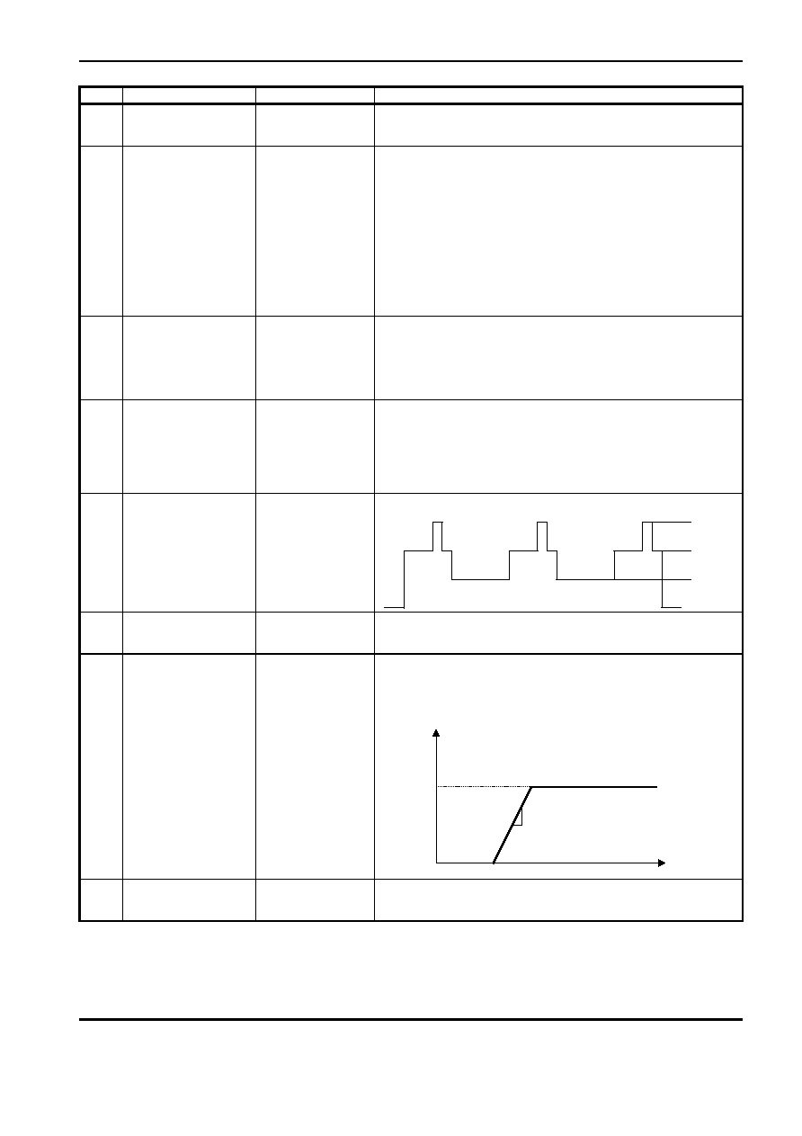
�
Ver3.7
00/01/28
50
Note
Items/Symbols
Bus conditoins
Measurement methods
D20
V. Ramp DC on
Service Mode
/ V
NOVRAMP
V STOP:1
Others:Preset
(1) Set V STOP to 1.
(2) Measure the DC level of Pin24, that is "V
NOVRAMP
".
D21
Vertical Pull-in Range
(Auto)
/ F
VPAUL
/ F
VPAUH
Vertical Pull-in Range
(50Hz)
/ F
VP50L
/ F
VP50H
Vertical Pull-in Range
(60Hz)
/ F
VP60L
/ F
VP60H
V-Freq:
000/001/010
Others:Preset
(6) Input a composite sync signal into Pin38.
(7) For V-Freq 000/001/010, increasing the input vertical period
from 220H by 0.5H step, measure the period at which input
signal synchronized with V Ramp(Pin24), that is "F
VPAUL
" /"
F
VP50L
"/ "F
VP60L
".
(8) (3)For V-Freq 000/001/010, decreasing the input vertical
period from 360H by 0.5H step, measure the period at which
input signal synchronized with V Ramp, that is "F
VPAUH
" /"
F
VP50H
"/ "F
VP60H
".
D22
Vertical Period on
Fixed Mode
/ T
V3125
/ T
V2625
/ T
V313
/ T
V263
V-Freq:
100/101/110/
111
Others:Preset
For V-Freq 100/101/110/111, measure the vertical period at SCP
out (Pin30), that is "T
V312.5
"/"T
V262.5
" / "T
V313
"/"T
V263
" .
D23
V-BLK Start Phase
/ PH
50VBLK
/ PH
60VBLK
V-BLK Width
/ W
50VBLK
/ W
60VBLK
All:Preset
(1)Input a 50Hz/60Hz composite sync signal into Pin38.
(2)Measure "T
50AFCOFF
" / "1T
60AFCOFF
" at Pin30. (cf. Fig.D25)
D24
Sand Castle Pulse
Level
/ V
SCPH
/ V
SCPM
/ V
SCPL
All:Preset
Measure "V
SCPH
" / "V
SCPM
" / "V
SCPL
" at Pin30.
V
SCPL
V
SCPM
V
SCPH
D25
Vertical Ramp
Amplitude
/ V
VRAMP
All:Preset
Measure the V Ramp amplitude at Pin24, that is "V
VRAMP
".
D26
Vertical AMP Gain
/ G
VAMP
Vertical AMP
Max.Output Level
/ V
VOMAX
Vertical AMP
Min.Output Level
/ V
VOMIN
All:Preset
(1)Let Pin26 be open.
(2)Changing the Pin25 DC voltage, measure "V
VOMAX
" / "V
VOMIN
" /
"G
VAMP
"
according to a following figure.
V
VOMAX
V
VOMIN
¢V=GVAMP
=20log(¢V#26/¢V#25)
#25DC
#26DC
D27
Vertical AMP
Max.Output Current
/ I
VOMAX
All:Preset
(1)Supply 7V to Pin25.
(2)Measure the current from Pin26 to GND, that is "I
VOMAX
".

�
Ver3.7
00/01/28
51
Note
Items/Symbols
Bus conditoins
Measurement methods
D28
Vertical NFB
Amplitude
/ V
NFB
Vertical Amplitude
Variable Range
/
∑
V
VRAMPH
/
∑
V
VRAMPL
V Size:0/32/63
Others:Preset
(1)Measure the amplitude of NFB V Ramp at Pin25, that is
"V
NFB
". (2)Measure the amplitude of NFB V Ramp at Pin25 for V-
Size 0/63, that is
V
NFBMIN
/ V
NFBMAX
.
(3)Calculate; "
∑
V
VRAMPH
"=(V
NFBMAX
-V
NFB
)/V
NFB
*100
"
∑
V
VRAMPL
"=(V
NFBMIN
-V
NFB
)/V
NFB
*100
D29
Vertical Linearity
Variable Range
/
∑
V
LIN1+
/
∑
V
LIN1-
/
∑
V
LIN2+
/
∑
V
LIN2-
V Linearity:0/8/15
Others:Preset
(1)For V Linearity 8, measure V
1
(from center to max.) and
V
2
(from center to min.) at Pin24 according to a follownig figure.
(2)For V Linearity 15/0, measure V
LIN1+
/ V
LIN1-
and V
LIN2+
/ V
LIN2-
.
(3)Calculate; "
∑
V
LIN1+
"=(V
LIN1+
-V
1
)/V1*100
"
∑
V
LIN1-
"=(V
LIN1
--V
1
)/V
1
*100
"
∑
V
LIN2+
"=(V
LIN2+
-V
2
)/V
2
*100
"
∑
V
LIN2-
"=(V
LIN2
--V
2
)/V
2
*100
V1
V2
Pin24
signal
D30
Vertical S Correction
Variable Range
/
∑
V
S1+
/
∑
V
S1-
/
∑
V
S2+
/
∑
V
S2-
V S Corr.:0/8/15
Others:Preset
(1)For V S Correction:8, measure V
1
and V
2
at Pin24 according to
a figure of NOTE:D32 .
(2)For V S Correction:15/0, measure V
S1+
/ V
S1-
and V
S2+
/ V
S2-
.
(3)Calculate; "
∑
V
S1+
"=(V
S1+
-V
1
)/V
1
*100
"
∑
V
S1-
"=(V
S1
--V
1
)/V
1
*100
"
∑
V
S2+
"=(V
S2+
-V
2
)/V
2
*100
"
∑
V
S2-
"=(V
S2
--V
2
)/V
2
*100
D35
Vertical Guard
Voltage
/ V
VG
All:Preset
Decreasing the Pin25 voltage from 5V, measure the voltage at
which Pin20 output drops to blanking level, that is "V
VG
".

�
Ver3.7
00/01/28
52
+
CE202:1 F
TB1254N
56
50
51
52
53
54
55
49
43
44
45
46
47
48
42
36
37
38
39
40
41
35
29
30
31
32
33
34
1
7
6
5
4
3
2
8
14
13
12
11
10
9
15
21
20
19
18
17
16
22
28
27
26
25
24
23
SDA
SCL
Y/C GND
Ys/Ym SW
EXT.R IN
RGB Vcc(9V)
R OUT
G OUT
B OUT
APC Filter
X'tal
H Vcc(9V)
V OUT
V NFB
IK IN
FBP IN/
SCP OUT
H OUT
Dig. GND
Dig. VDD
DC Restor
H.AFC Filter
ABCL IN
BLACK Det
Y/C Vcc(5V)
PIF tank
IF DET OUT
AFT OUT
C IN
SIF IN∑^
H CORRECTION IN
DE-EMP.
Sync IN
RIPPLE FIL
AUDIO OUT
IF AGC
IF GND
IF IN
IF IN
IF Vcc
LOOP Filter
NC
Y IN
DC NF
+
+
+
+
+
+
+
+
+
SAW
Reg.
+
+
+
+
+
+
+9V
+5V
+9V
8
7
6
5
4
3
2
1
9
10
11
12
13
14
15
16
TC4538BP
8
7
6
5
4
3
2
1
9
10
11
12
13
14
TC74HC125P
N.C.
N.C.
SDA
SCL
H IN
FBP
TB1254N TEST CIRCUIT
+
9
17
14
7
21
C2:0.01 F
R7:
430∂
C5:
0.01 F
C6:0.01 F
CE8:2.2 F
R10:33k∂ CE9:0.22 F
C7:2200pF
X1:
4.433619MHz C8:9pF
C10:0.1 F
C11:0.1 F
C12:0.1 F
R14:75∂
R13:75∂
R12:75∂
C9:0.01 F
CE10:100 F
CE31:0.47 F
R39:100∂
R38:100∂
CE13:100 F
C16:0.01 F
R52:
4.7k∂
R53:
4.7k∂
R50:51k∂
CE24:10 F
R51:
51k∂
VR1:
50kB
C30:1000pF
VR2:
50kB
C29:1000pF
CE25:100 F
C31:0.01 F
CE26:47 F
C32:0.01 F
CE27:100 F
C019:
0.01 F
R36:
390∂
R37:
91∂
R206:270
CE19:0.22 F
CE21:1 F
R40:0pen
CE16:1 F
C23:0.1 F
C021:0.01 F
CE20:100 F
R42:3k∂
R43:2k∂
R41:470∂ CE22:0.22 F
C24:1000pF
CE23:10 F
CE3:
22 F
C28:0.01 F
R49:1k∂
R44:
330∂
L4:15 H
R46:
1k∂
R45:
330∂
Q14:
F1:Trap
L1:12 H
CE28:47 F
U IN
V IN
ref R
V RAMP
CW OUT
RF AGC
PIF tank
SIF OUT
EXT.G IN
EXT.B IN
R15:100∂
R16:3k∂
+
+
C27:0.01 F
R47:51∂
C26:0.1 F
+
CE15:100 F
C18:0.01 F
R17:100∂
R19:100∂
R18:3k∂
R20:3k∂
+
CE17:100 F
R21:100∂
+
R25:
1.2k∂
R27:510∂
R28:1.2k∂
R24:100∂
R22:100∂
R23:10k∂
CE11:100 F
R26:510∂
CE4:100 F
CE18:1 F
C20:0.1 F
C22:0.1 F
+
C25:0.01 F
R48:1k∂
Reg.
+
+
+5V
+9V
CE29:
47 F
CE30:100 F
C33:
0.01 F
Reg.
+
+
+5V
+9V
CE1:47 F
CE2:100 F
C1:0.01 F
+
CE7:4.7 F
R8:33k∂
+
+
ZD1:
4.7v
MON OUT
TV IN
EXT IN
+
CE201:1 F
R202:
1k∂
R201:
1k∂
R203:
2k∂
+
CE203:4.7 F
EXT AUDIO
R205:680∂
R204:75∂
CE5:
CE6:
C3:
C4
R1:
R2:
R3:
R4:
R5:
R6:
R11:
Q201
L2:
Q2:
Q1:
T1:
Q3:
Q4:
Q5:
Q6:
Q7:
Q8:
Q9:
SW2:
SW3:
P2
P3
Q15:
SW6:
T2:
F2:
BPF
P1:
R300:10k∂
75∂
75∂
C302:
0.01 F
C13:8200pF
R32:1k∂
R31:510∂
R30:1k∂
C14:0.47 F
Q10:
R35:8.2k∂
CE14:0.22 F
C17:
8200pF
+
R34:15k∂
R29:5.6k∂,1%
C106:2200pF
R33:10k∂
C15:0.1 F
D1:

�
Ver3.7
00/01/28
53

�
Ver3.7
00/01/28
54
+
CE202:1 F
TB1254N
56
50
51
52
53
54
55
49
43
44
45
46
47
48
42
36
37
38
39
40
41
35
29
30
31
32
33
34
1
7
6
5
4
3
2
8
14
13
12
11
10
9
15
21
20
19
18
17
16
22
28
27
26
25
24
23
SDA
SCL
Y/C GND
Ys/Ym SW
EXT.R IN
RGB Vcc(9V)
R OUT
G OUT
B OUT
APC Filter
X'tal
H Vcc(9V)
V OUT
V NFB
IK IN
FBP IN/
SCP OUT
H OUT
Dig. GND
Dig. VDD
DC Restor
H.AFC Filter
ABCL IN
BLACK Det
Y/C Vcc(5V)
PIF tank
IF DET OUT
AFT OUT
C IN
SIF IN∑^
H CORRECTION IN
DE-EMP.
Sync IN
RIPPLE FIL
AUDIO OUT
IF AGC
IF GND
IF IN
IF IN
IF Vcc
LOOP Filter
NC
Y IN
DC NF
+
+
+
+
+
+
+
+
+
SAW
Reg.
+
+
+
+9V
+5V
+9V
TB1254N APPLICATION CIRCUIT
+
C2:0.01 F
R7:
430∂
C5:
0.01 F
C6:0.01 F
CE8:2.2 F
R10:33k∂ CE9:0.22 F
C7:2200pF
X1:
4.433619MHz C8:9pF
C10:0.1 F
C11:0.1 F
C12:0.1 F
R14:75∂
R13:75∂
R12:75∂
C9:0.01 F
CE10:100 F
CE31:0.47 F
R39:100∂
R38:100∂
100 F
0.01 F
CE26:47 F
C32:0.01 F
CE27:100 F
C019:0.01 F
R36:
390∂
R37:
91∂
R206:270
CE19:0.22 F
CE21:1 F
R40:0pen
CE16:1 F
C23:0.1 F
C021:0.01 F
CE20:100 F
R42:3k∂
R43:2k∂
R41:470∂ CE22:0.22 F
C24:1000pF
CE23:10 F
CE3:
22 F
C28:0.01 F
R49:1k∂
R44:
330∂
L4:15 H
R46:
1k∂
R45:
330∂
Q14:
F1:Trap
L1:12 H
U IN
V IN
ref R
V RAMP
CW OUT
RF AGC
PIF tank
SIF OUT
EXT.G IN
EXT.B IN
R15:100∂
R16:3k∂
+
+
C26:0.1 F
+
CE15:100 F
C18:0.01 F
R17:100∂
R19:100∂
R18:3k∂
R20:3k∂
+
CE17:100 F
R21:100∂
CE4:100 F
CE18:1 F
C20:0.1 F
C22:0.1 F
+
C25:0.01 F
R48:1k∂
Reg.
+
+5V
+9V
CE2:100 F
C1:0.01 F
+
CE7:4.7 F
R8:33k∂
+
+
ZD1:
4.7v
MON OUT
TV IN
EXT IN
+
CE201:1 F
R202:
1k∂
R201:
1k∂
R203:
2k∂
+
CE203:4.7 F
EXT AUDIO
R205:680∂
R204:75∂
CE5:
CE6:
C3:
C4
R1:
R2:
R3:
R4:
R5:
R6:
R11:
Q201
L2:
Q2:
Q1:
T1:
Q3:
P2
Q15:
T2:
F2:
BPF
P1:
R300:10k∂
75∂
75∂
C302:
0.01 F
C13:8200pF
R32:1k∂
R31:510∂
R30:1k∂ C14:0.47 F
Q10:
R35:8.2k∂
CE14:0.22 F
C17:
8200pF
+
R34:15k∂
R29:5.6k∂,1%
C106:2200pF
R33:10k∂
C15:0.1 F
D1:
+
+9V
+
+9V
100 F
0.01 F
100 F
0.01 F

�
Ver3.7
00/01/28
55
OUTLINE DRAWING
Unit : mm
SDIP56-P-600-1.78

�
Ver3.7
00/01/28
56
∑∑∑∑
∑∑∑
∑∑∑
p.1
IF stage
for L system,AM sound demodulation
∑∑
Chroma stage
U/V input ports
Cb/Cr input ports
P.2
Block Diagram Pin9
RFAGC/SIF in
RF AGC
Ripple filter
BIAS
L-SECAM AM
∑∑
H.AFC
∑∑∑∑∑∑
∑∑∑∑∑∑
P.3
Pin3 SIF OUT Interface
3
5
14
100∂
500∂
15k∂
9V
8.3k∂
8.3k∂
3
5
14
100∂
500∂
15k∂
9V
16.3k∂
16k∂
Pin4 Audio out Interface
4
5
14
50k∂
4.5V
ATT
9V
30k∂
4
5
14
50k∂
5.3V
ATT
9V
30k∂
100∂
P.3
Pin6,7 IF IN
90dB
∑
90dB(
∑
V)(Pin6-7)
field intensity
level
P.4
Pin8 RF AGC/SIF IN
RF AGC/SIF IN
RF AGC
This terminal also lead to 1'st SIF
input pole.
∑∑

�
Ver3.7
00/01/28
57
8
5
14
5V
300∂
30k∂
30k∂
to SELF ADJ
5
1
500∂
10k∂
9
5
14
9V
300∂
30k∂
30k∂
to SELF ADJ
P.4
Pin10 IF AGC
2.2mF
2.2
∑
F
P.8
Pin36 Black DET
36
2.5V
19
42
4k∂
36
2.5V
19
42
4k∂
P.9
Pin40 DC restor
40
19
42
10k
50k
40
19
42
10k
50k
Pin38 Sync in
1401IRE
140IRE
p.10
Pin44,45 U/V in
U/V in
Cb/Cr in
P.11
Pin50,51 PIF tank
27pF
18pF
p.14
RF AGC
RF AGC delay point
RF AGC delay point (Pin6-7)
01:
65dBm
01: 65 dB(
∑
V)
3F:
100dBm
3F: 100 dB(
∑
V)
P.15
DDS MODE SW
∑∑∑
p.16
Split / Inter
∑∑∑
∑∑
p.17
U/V SW
U/V
Cb/Cr
p.18
Self Test
01:B OUT
10:R OUT
∑∑
p.19
Self Adj.
Self Adj.
Self Test

�
Ver3.7
00/01/28
58
00: AFT (Normal) 10: RF AGC X
1/2
Noise Det
∑
p.22 (*3)
(*3)Pin 1, 4, 5, 11, 12, 19, 26, 33, 34,
35, 42, 50, 51 are weak against
∑...
(*3)Pin 1, 4, 5, 6, 9, 11, 12, 13, 19, 26,
31, 32, 33, 34, 35, 37, 42, 43, 50, 51
are weak against
∑...
p.29
T4,T5
Cut off/Drive
∑
spec.
∑∑
∑∑∑
T5 spec.
∑∑
Drive
∑
spec.
∑∑
min. typ. max.
3 3.5 4
-6.0 -5.5 -5.0
Drive
∑
spec.
∑∑
min. typ. max.
2.5 3.5 4.5
-8.0 -5.5 -4.5
T18
∑∑
p.35
S2
Input a signal that 4.5[MHz],
100[dB
V], 2.5[kHz]
...∑
Input a signal that 4.5[MHz],
100[dB
V], 25[kHz]
...∑
S3
Input a signal that 4.5[MHz],
100[dB
V], 2.5[kHz]
...∑
Input a signal that 4.5[MHz],
100[dB
V], 25[kHz]
...∑
p.36
S8
Input a signal that 4.5[MHz],
100[dB
V], 2.5[kHz]
...∑
Input a signal that 4.5[MHz],
100[dB
V], 25[kHz]
...∑
p.48
T18
∑∑
p.54
pin9
RF AGC/SIF IN
RF AGC
Pin2 Ripple filter
10
∑
F
22
∑
F
p.55
Pin9
RF AGC/SIF IN
RF AGC