 | –≠–ª–µ–∫—Ç—Ä–æ–Ω–Ω—ã–π –∫–æ–º–ø–æ–Ω–µ–Ω—Ç: TB2913HQ | –°–∫–∞—á–∞—Ç—å:  PDF PDF  ZIP ZIP |

TB2913HQ(o)
2004-03-01
1
TOSHIBA Bi-CMOS Digital Integrated Circuit Silicon Monolithic
TB2913HQ
Maximum Power 47 W BTL ◊ 4-ch Audio Power IC
The TB2913HQ is 4-ch BTL audio amplifier for car audio applications.
This IC can generate higher power: P
OUT
MAX = 47 W as it
includes the pure complementary P-ch and N-ch DMOS output
stage.
It is designed to yield low distortion ratio for 4-ch BTL audio
power amplifier, built-in standby function, muting function, and
various kinds of protectors.
Additionally, Clip detector is built in.
Features
∑ High power output
: P
OUT
MAX (1) = 47 W (typ.)
(V
CC
= 14.4 V, f = 1 kHz, JEITA max, R
L
= 4 )
: P
OUT
MAX (2) = 43 W (typ.)
(V
CC
= 13.7 V, f = 1 kHz, JEITA max, R
L
= 4 )
: P
OUT
(1) = 29 W (typ.)
(V
CC
= 14.4 V, f = 1 kHz, THD = 10%, R
L
= 4 )
: P
OUT
(2) = 25 W (typ.)
(V
CC
= 13.2 V, f = 1 kHz, THD = 10%, R
L
= 4 )
∑ Low distortion ratio: THD = 0.015% (typ.)
(V
CC
= 13.2 V, f = 1 kHz, P
OUT
= 5 W, R
L
= 4 )
∑ Low noise: V
NO
= 90 µVrms (typ.)
(V
CC
= 13.2 V, R
g
= 0 , BW = 20 Hz~20 kHz, R
L
= 4 )
∑ Built-in standby switch function (pin 4)
∑ Built-in muting function (pin 22)
∑ Built-in Clip-detection function (pin 25)
∑ Built-in various protection circuits:
Thermal shut down, overvoltage, out to GND, out to V
CC
, out to out short
∑ Operating supply voltage: V
CC (opr)
= 9~18 V (R
L
= 4 )
Note 1: Since this device's pins have a low withstanding voltage, please handle it with care.
Note 2
: Install the product correctly. Otherwise, it may result in break down, damage and/or degradation to the
product or equipment.
Note 3: These protection functions are intended to avoid some output short circuits or other abnormal conditions
temporarily. These protect functions do not warrant to prevent the IC from being damaged.
- In case of the product would be operated with exceeded guaranteed operating ranges, these protection
features may not operate and some output short circuits may result in the IC being damaged
Weight: 7.7 g (typ.)

TB2913HQ(o)
2004-03-01
2
Block Diagram
Note: Some of the functional blocks, circuits, or constants in the block diagram may be omitted or simplified for
explanatory purpose
R
L
R
L
R
L
11
9
8
7
5
2
3
17
18
19
21
24
23
12
15
14
1
20
6
R
L
IN1
IN2
IN3
IN4
13
C
1
C
1
C
1
C
1
PRE-GND
10
25
22
OUT1 (
+
)
PW-GND1
OUT1 (
-
)
OUT2 (
+
)
PW-GND2
OUT2 (
-
)
OUT3 (
+
)
PW-GND3
OUT3 (
-
)
OUT4 (
+
)
PW-GND4
OUT4 (
-
)
TAB
V
CC1
V
CC2
C
3
C
4
C
2
: PRE-GND
: PW-GND
STBY
RIP
MUTE
C
5
16
C
6
4
Clip
DET
MUTE
PLAY
5 V
R
1
AC-GND

TB2913HQ(o)
2004-03-01
3
Caution and Application Method
(Description is made only on the single channel.)
1. Voltage
Gain
Adjustment
This IC has no NF (negative feedback) Pins. Therefore, the voltage gain can not be adjusted, but it makes
the device a space and total costs saver.
The voltage gain of amp.1
: G
V1
= 0dB
The voltage gain of amp.2A, B
: G
V2
= 20dB
The voltage gain of BTL connection : G
V (BTL)
= 6dB
Therefore, the total voltage gain is decided by expression below.
G
V
= G
V1
+ G
V2
+ G
V (BTL)
= 0 + 20 + 6 = 26dB
2. Standby
SW
Function
(pin 4)
By means of controlling pin 4 (standby pin) to
High and Low, the power supply can be set to ON
and OFF. The threshold voltage of pin 4 is set at
about 3V
BE
(typ.), and the power supply current is
about 2 µA (typ.) in the standby state.
Control Voltage of Pin 4: V
SB
Standby Power V
SB
(V)
ON OFF 0~1.5
OFF ON
3.5~6
V
When changing the time constant of pin 4, check the
pop noise.
Advantage of Standby SW
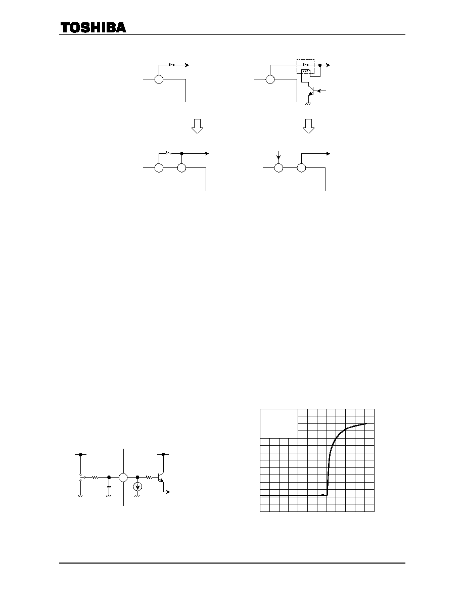
(1) Since
VCC can directly be controlled to ON or OFF by the microcomputer, the switching relay can be
omitted.
(2) Since the control current is microscopic, the switching relay of small current capacity is satisfactory
for switching.
Amp. 1
Input
Amp. 2A
Amp. 2B
Figure 1 Block Diagram
Figure 2 With pin 4 set to High,
Power is turned ON
ON
4
OFF
10 k
to BIAS
CUTTING CIRCUIT
2 V
BE
V
CC
Power
TB2913HQ(o)
2004-03-01
4
3. Muting
Function
(pin 22)
Audio muting function is enabled when pin 22 is Low. When the time constant of the muting function is
determined by R
1
and C
4,
it should take into account the pop noise. The pop noise, which is generated when
the power or muting function is turned ON/OFF, will vary according to the time constant. (Refer to Figure 4
and Figure 5.)
The pin 22 is designed to operate off 5 V so that the outside pull-up resistor R
1
is determined on the basic of
this value:
ex) When control voltage is changed in to 6 V from 5 V.
6 V/5 V ◊ 47 k = 56 k
Additionally, as the V
CC
is rapidly falling, the IC internal low voltage muting operates to eliminate the
large pop noise basically.
The low voltage muting circuit pull 200uA current into the IC so that the effect of the internal low
voltage muting does not become enough if the R1 is too small value.
To obtain enough operation of the internal low voltage muting, a series resistor, R
1
at pin 22 should be
47 k or more.
V
CC
Small current capacity switch
Battery
Stand-By
V
CC
From microcomputer
Battery
Stand-By
≠ Standby Switch Method ≠
Figure 3
≠ Conventional Method ≠
V
CC
Large current capacity switch
Battery
V
CC
From
microcomputer
Battery
Relay
Figure 5 Mute Attenuation
-
V
MUTE
(V)
Pin 22 control voltage: VMUTE (V)
ATT ≠ V
MUTE
Mut
e
a
tte
nu
a
t
io
n
AT
T
(d
B
)
Figure 4 Muting Function
0
-
120
-
100
-
80
-
60
-
40
-
20
0
20
0.5
1
1.5
2 2.5 3
V
CC
=
13.2 V
f
=
1kHz
R
L
=
4
V
OUT
=
20dBm
22
1 k
R
1
5 V
Mute ON/OFF
control
C
4

TB2913HQ(o)
2004-03-01
5
4.
Output Clip Detection Function
(pin 25)
The output clip detection terminal of pin 25 has the open collector output structure on chip as shown in
Figure 6. In case that the output waveform is clipping, the clip detection circuit is operated and NPN Tr. is
turned on.
It is possible to improve the audio quality with controlling the volume, tone control circuit through L.P.F.
smoothing circuit as shown in Figure 7.
In case of being unused this function, use this IC as open connection on pin 25.
(A)
5 V
t
AC
(A) Output (AC wave form)
(B)
t
DC
(B) Clip Detector Circuit
(internal)
(C)
t
DC
(B) Clip Detector Terminal
(pin 25)
GND
Figure 7 Clip Detection
Figure 6
pin 25: Open collector output (active low)
OUTPUT CLIP
DETECTOR
25
5 V
L.P.F.
SMOOTHING
CIRCUIT
VOLUME CONTROL CIRCUIT
TONE CONTROL CIRCUIT
(Application)