
TB62709NG/FG
TOSHIBA
Bi-CMOS INTEGRATED CIRCUIT SILICON MONOLITHIC
TB62709NG,TB62709FG
7-SEGMENT DRIVERS WITH BUILT-IN DECODERS
(COMMON ANODE CAPABILITY, MAXIMUM 4-DIGIT CONTROL)
The TB62709NG and TB62709FG are multifunctional, compact,
7-segment LED display drivers.
These ICs can directly drive 7-segment displays and individual
LEDs, and can control either a 4-digit display with decimal
points, or 32 individual LEDs.
These ICs can also be used with common-anode displays. Their
outputs are constant current, the ampere levels at which are set
using an external resistor.
A synchronous serial port connects the IC to the CPU.
The different modes of control provided by this device including
Duty Control Register Set, Digit Set, Decode Set and Standby Set,
are all based on every 16-bit of serial data.
This devices are a product for the Pb free(Sn-Ag).
FEATURES
Control circuit power supply voltage
:
V
DD
= 4.5 to 5.5 V
Digit output rating
: 17 V / -400 mA
Decoder output rating
: 17 V / 50 mA
Built-in decoder
: Decodes the numerals 0 to 9, certain alphabetic
characters, and of course blanks code.
Digit control function
: Can scan digit outputs DIG-0 to DIG-3 when connected
to the common anode pins of a 7-segment display.
Maximum transmission frequency
:
f
CLK
= 15 MHz
Decoder outputs (OUT-A to OUT-Dp)
Output current can be set up to a 40mA maximum using an external resistor.
Constant current tolerance (Ta = 25�C, V
DD
= 5.0 V)
: Variation between bits = �7%, variation between devices
(including variation between bits) = �15% at V
CE
0.7 V
Package
:
24-pin SDIP (SDIP24-P-300-1.78)
24-pin SSOP (SSOP24-P-300-1.00)
TB62709NG
TB62709FG
Weight
SDIP24-P-300-1.78 : 1.62 g (typ.)
SSOP24-P-300-1.00 : 0.32 g (typ.)
Web: www.marktechopto.com | Email: info@marktechopto.com
Company Headquarters
3 Northway Lane North
Latham, New York 12110
Toll Free: 800.984.5337
Fax:
518.785.4725
California Sales Office:
950 South Coast Drive, Suite 2
25
Costa Mesa, California 92626
Toll Free: 800.984.5337
Fax: 714.850.9314

TB62709NG/FG
2005-10-06
2
PIN ASSIGNMENT
(Top view)
BLOCK DIAGRAM

TB62709NG/FG
2005-10-06
3
PIN FUNCTIONS
PIN NUMBER
PIN NAME
FUNCTION
1 V
DD
5 V power pin.
2 DATA-IN (DI)
Serial data input pin.
3
CLOCK (CK)
Clock input pin. The shift register shifts data on the clock's rising edge.
4 LOAD
(LD)
Load signal input pin. The data in the D
8
to D
15
are read on the rising edge and the current
load register the is selected from among the Duty Register, the Decode & Digit Register, or
Data Registers 0 to 3. The D
0
to D
7
bits of the 16-bit shift register contain data corresponding
to the same registers just described, which are read on the load signal's falling edge.
5~12
OUT-A to
OUT-Dp
Segment drive output pins. The A to Dp outputs correspond to the seven segments. These
pins output constant sink current. Connect each of these pins to the corresponding LED's
cathode.
13, 21
P-GND
Ground pins, There are two which can be used to ground the output OUT-A to OUT-Dp pins.
14 TEST-IN2
Product test pin. In normal use, be sure to connect to ground.
15 TEST-IN1
Product test pin. In normal use, be sure to connect to ground.
16, 17, 19, 20 DIG-0 to DIG-3
Digit output pins. Each of these pins can control one of the four seven-segment digits in a
display.
These pins output the V
CC
pin voltage as a source current output. Connect these pins to the
LED anodes.
18 V
CC
Power pin for digit output.
22 R-EXT
Current setting pin for the OUT-A to OUT-Dp pins. Connect a resistor between this pin and
ground when setting the current.
23 DATA-OUT (DO) Serial data output pin. Use when TB62709N or TB62709F devices are used in cascade
connections.
24 L-GND
Ground pin for logic and analog circuits.

TB62709NG/FG
2005-10-06
4
TIMING DIAGRAM
DATA INPUT
Transfer data to the DATA-IN pin on every 16-bit combining address (8bits) and data (8bits). After the 16
th
clock signal input following this data transfer input a load signal from the LD pin.
Input the load signal using an Active High pulse. The register address is set on the rising edge of the load pulse.
On the subsequent falling edge, the data are read as data of the mode of the register.

TB62709NG/FG
2005-10-06
5
DESCRIPTION OF OPERATION
Data input (SERIAL-IN, CLOCK, LOAD)
The data are input serially using the SERIAL-IN pin. The data input interface consists of a total of three
inputs : SERIAL-IN, LOAD, and CLOCK.
Binary code stored in the 16-bit shift register offers control modes including duty Control Register Set, Digitset,
Decode Set, and Standby Set,
The data are shifted on the rising edge of the clock, starting from the MSB. Cascade-connecting TB62709NG or
TB62709FG devices provides capability for controlling a larger number of digits.
The serial data in the 16-bit shift register are used as follows : the four bits D
15
(MSB) to D
12
select the IC
operating mode (Table 1), while D11 to D
8
select the register corresponding to the operating mode (Table 2).
Bits D
7
to D
0
(LSB) of the 16-bit shift register are used for detail settings, such as number of digits in use,
character settings in each digit, and light intensity.
The internal registers are loaded on the rising edge of the LOAD signal, which causes loading of data from an
external source into the D
15
(MSB) to D8 bits of the shift register, operating mode and the corresponding
register selection data. On the subsequent falling edge, the detail setting data of D
7
to D0 (LSB) are loaded.
Normally LOAD is Low. After a serial transfer of 16bits, the input of a High-level pulse loads the data.
Note the following caution : Use the D
15
to D
8
setting and the D
7
to D
0
detail data setting as a pair. If only the
D
7
to D
0
data are input without setting D
15
to D
8
an error condition may result, in which the device will not
operate normally. If the current mode is set again by a new signal, the data for D
15
to D
8
must also be re-input.
Operating precautions
At power-on or after operation in Clear mode (in initial state), set the IC to Normal mode again. Otherwise, the
IC will not drive the LED.
Operating the IC in Blank mode (all lights off) or in All On mode (all lights lit) does not affect the internal data.
Setting the IC to Normal mode again continues the LED lighting in the state governed by the settings made
immediately before mode change.
Normal mode (not Shut Down, Clear, Blank, or All On mode) continues the operations set in Load Register
mode. In Normal mode, operations are governed by any new settings made in the Load Register, as soon as the
changed setting values are loaded.

TB62709NG/FG
2005-10-06
6
Operating modes (Table 1.)
These ICs support the following five operating modes :
1. Blank
: Forcibly turns OFF the constant-current output both for data and for digit setting. This
mode is not affected by the values in bits D
11
to D
0
.
2. Normal Operate : Used for display operations after the settings of the digits are complete. Note that setting
this mode without making any other settings will cause display of the numeral 0.
3. Load Register : Used for the detail settings of the Duty Control Register, for setting Decode / No Decode,
for inputting display data, and for setting the number of digits to drive. D
11
to D
0
of the
shift register are used for the detail settings of the digits currently being driven (Table 2).
4. All On
: Forcibly turns ON the data-side constant-current output. This mode is not affected by
D
11
to D
0
.
The initial setting is four digits. When the digits must be changed,
use Load Register mode to set the number of digits to drive.
5. Standby
: Used to set Standby state (in which internal data are not cleared) and to clear data
(initialization). The settings in D
3
to D
0
of the shift register determine the choice between
standby state or initialization.
Table 1 Operating mode settings
REGISTER DATA
D
15
D
14
D
13
D
12
D
11
~D
8
D
7
~D
4
D
3
~D
0
HEX CODE
INITIAL
SETTING
BLANK (OUT-n &
DIG-0~3 ALL-OFF)
0 0 0 0
0---H
NORMAL (OPERATION)
0
0
0
1
1---H
LOAD REGISTER (DUTY,
DECODE, DIGIT & DATA)
0 0
1
0 X X X 2XXXH
ALL ON (OUTn ALL-ON) 0 0 1 1
3---H
STAND-BY 0
1
0
0
X 4--XH
X = Input H or L. "-" = Are not affected by the truth table.

TB62709NG/FG
2005-10-06
7
Load Register Selection modes (Table 2)
These modes select the register to provide the data to control the IC operation. The Load Register selection
mode is determined by the settings of D
15
to D
12
and D
11
to D
8
of the shift register.
1. Duty Register
: The data in D
7
to D
0
of this register set the digit output duty cycle.
Duty settings can be made in 16 steps from 0 / 16 to 15 / 16.
(See Table 3)
2. Decode & Digit Register : Sets Decode / No Decode and the number of digits to drive. Decode can be set
using
D
7
to D
4
.
The number of digits driven can be set using D
3
to D
0
. Decode / No Decode and
the number of digits driven are set simultaneously.
3. Data registers 0 to 3
: Set the display data corresponding to DIG0 to DIG3 respectively.
D
7
to D
0
of the shift register are used to set the display data.
Table 2 Load register selection
REGISTER DATA
D
15
~D
12
D
11
D
10
D
9
D
8
D
7
~D
4
D
3
~D
0
HEX
CODE
LOAD DUTY REGISTER
2H
0
0
0
0
X
X
20XXH
LOAD DECODE & DIGIT REGISTER
2H
0
0
0
1
X
X
21XXH
LOAD DATA REGISTER 0
2H
0
0
1
0
X
X
22XXH
LOAD DATA REGISTER 1
2H
0
0
1
1
X
X
23XXH
LOAD DATA REGISTER 2
2H
0
1
0
0
X
X
24XXH
LOAD DATA REGISTER 3
2H
0
1
0
1
X
X
25XXH
X = Input H or L.

TB62709NG/FG
2005-10-06
8
DUTY CONTROL REGISTER SETTINGS
Duty Control Register detail settings and operation (Table 3)
Writing 20H to D
15
~D
8
and writing 0~FH to D
3
~D
0
sets the duty cycle shown in the following table for the
digit-side source driver output. The duty cycle can be set in 16 steps.
The initial setting is 15 / 16. After Data Clear, the setting is also 15 / 16.
The current settings continue until changed (by reset execution, or to the initial state, Data Clear state, or
standby state).
Table 3 Duty control register settings
REGISTER DATA
DUTY CYCLE
D
15
~D
8
D
7
~D
4
D
3
D
2
D
1
D
0
HEX
CODE
INITIAL SETTING
0 / 16
20H
0 0 0 0 20X0H
1 / 16
20H
0 0 0 1 20X1H
2 / 16
20H
0 0 1 0 20X2H
3 / 16
20H
0 0 1 1 20X3H
4 / 16
20H
0 1 0 0 20X4H
5 / 16
20H
0 1 0 1 20X5H
6 / 16
20H
0 1 1 0 20X6H
7 / 16
20H
0 1 1 1 20X7H
8 / 16
20H
1 0 0 0 20X8H
9 / 16
20H
1 0 0 1 20X9H
10 / 16
20H
1 0 1 0 20XAH
11 / 16
20H
1 0 1 1 20XBH
12 / 16
20H
1 1 0 0 20XCH
13 / 16
20H
1 1 0 1 20XDH
14 / 16
20H
1 1 1 0 20XEH
15 / 16
20H
1 1 1 1 20XFH
X = Input H or L. "-" = Are not affected by the truth table.

TB62709NG/FG
2005-10-06
9
DIGIT SETTINGS
Setting the number of digits (Table 4)
Writing 21H to D
15
~D
8
and at the same step writing 0H~3H to D
3
~D
0
sets the number of digits to a maximum
of four the display. The initial setting is four digits, and four will also be set by a Data Clear.
The current settings continue until changed (by reset execution, or to the initial state, Data Clear state, or
standby state).
When changing the number of digits, also set D
7
to D
4
.
Table 4 Digit settings
REGISTER DATA
D
15
~D
8
D
7
~D
4
D
3
D
2
D
1
D
0
HEX
CODE
INITIAL
SETTING
ACTIVATED DIG--0
ONLY
21H
X 0 0 0 0
21X0H
ACTIVATED DIG--0~1
21H
X 0 0 0 1
21X1H
ACTIVATED DIG--0~2
21H
X 0 0 1 0
21X2H
ACTIVATED DIG--0~3
21H
X 0 0 1 1
21X3H
X = Input H or L.
DECODE SETTINGS
Decode settings (Table 5)
The settings for Decode are the same as the settings for the number of digits, described under setting, above.
Writing 21H to D
15
~D
8
and writing 0~1H to D
7
~D
4
set Decode mode.
When using this IC for controlling the lighting on individual LEDs used for a dot matrix rather than a
7-segment display, set to No Decode.
As Table 6 shows, D
0
in the data register is used to turn OUT-a ON and OFF ; D
1
turns OUT-b ON and OFF.
The initial setting is Decode mode, and Decode mode will also be set by a Data Clear.
The current settings continue until changed (by reset execution, or to the initial state, Data Clear state, or
standby state).
Since D
3
to D
0
are also used for setting the number of digits, when changing the Decode setting, also set D
3
to
D
0
.
Table 5 Decode settings
REGISTER DATA
D
15
~D
8
D
7
D
6
D
5
D
4
D
3
~D
0
HEX CODE
INITIAL
SETTING
PASS DECODER (NO DECODE)
21H
0
0
0
0
X
210XH
DECODE
21H
0 0 0 1 X 211XH
X = Input H or L.

TB62709NG/FG
2005-10-06
10
THE FOLLOWING TABLE SHOWS THE CORRESPONDENCE BETWEEN THE SERIAL
DATA AND THE OUTPUT PINS WHEN NO DECODE IS SET
Table 6 Correspondence between serial data and output pins in no decode mode
REGISTER DATA
OUTPUT
INITIAL STATE
NOTE
D
0
OUT-a L
D
1
OUT-b L
D
2
OUT-c L
D
3
OUT-d L
D
4
OUT-e L
D
5
OUT-f L
D
6
OUT-g L
D
7
OUT-Dp L
Output is ON when data
= H and OFF when data
= L.
STANDBY SETTINGS
Standby mode settings and operation (Table 7)
Writing 4H to D
15
~D
12
and writing 0H to D
3
~D
0
sets Standby mode. Writing 4H to D
15
~D
12
and writing 1H to
D
3
~D
0
sets All Data Clear mode.
Standby mode maintains the settings made immediately before this mode came in force, turns the output
current OFF, and controls the bias current flowing in the internal circuits. All Data Clear resets all settings to
their initial states.
Table 7 Standby settings
REGISTER DATA
D
15
~D
8
D
7
~D
4
D
3
D
2
D
1
D
0
HEX
CODE
STANDBY (NO DATA CLEAR)
4-H
0 0 0 0 4XX0H
ALL DATA CLEAR
4-H
0 0 0 1 4XX1H
X = Input H or L. "-" Are not affected by the truth table.

TB62709NG/FG
2005-10-06
11
LIST OF CHARACTER GENERATOR DECODING DATA
Character generator decoding (Table 8)
As the following table shows, the characters are decoded using combinations of the data in D
0
to D
3
and D
5
to
D
4
. In decoding, D
6
is used exclusively for setting decimal points.
Spaces where (D
0
, D
1
, D
2
, D
3
) = (0000) and (D
5
, D
4
) = (01) are regarded as blank.
Table 8 List of character generator decoding data
D
0
0 1 0 1 0 1 0 1 0 1 0 1 0 1 0 1
D
1
0 0 1 1 0 0 1 1 0 0 1 1 0 0 1 1
D
2
0 0 0 0 1 1 1 1 0 0 0 0 1 1 1 1
D
3
0 0 0 0 0 0 0 0 1 1 1 1 1 1 1 1
D
5
D
4
HEX
0 1 2 3 4 5 6 7 8 9 A B C D E F
0
0
0
0
1
1
D
7
D
6
X
0
Dp OFF
X
1
Dp ON

TB62709NG/FG
2005-10-06
12
DATA INPUT
(Example 1: Displays and blinks characters a, b, c and d in digits 0, 1, 2 and 3 respectively.
Period after "d" part of it, or a sentence-end marker?
)
STEP
D15~
D12
D11~
D8
D7~
D4
D3~
D0
DIG
-0~3
SEG
-a, b, c, d, e, f, g
SEG
-Dp
MODE
DISPLAY
INDICATE
0
OFF
OFF
OFF
At power-on
( = CLEAR MODE)
ALL BLANK
1
0010
0000
XXXX
1111
OFF
OFF
OFF
DUTY = 15 / 16
ALL BLANK
2
0010
0001
0001
0011
OFF
OFF
OFF
DECODE, 4DIG
ALL BLANK
3 0010
0010
X000
1010 OFF
OFF
OFF
DIG-0 = a
ALL BLANK
4 0010
0011
X000
1011 OFF
OFF
OFF
DIG-1 = b
ALL BLANK
5 0010
0100
X000
1100 OFF
OFF
OFF
DIG-2 = c
ALL BLANK
6 0010
0101
X000
1101 OFF
OFF
OFF
DIG-3 = d
ALL BLANK
7 0001
XXXX
XXXX
XXXX ON
ON
OFF
NORMAL
a-b-c-d
8
0010
0000
XXXX
1000
ON
ON
OFF
DUTY = 8 / 16
a-b-c-d
9 0000
XXXX
XXXX
XXXX
OFF
OFF
OFF
BLANK
ALL
BLANK
10 0001
XXXX
XXXX
XXXX ON
ON
OFF
NORMAL
a-b-c-d
11 0000
XXXX
XXXX
XXXX OFF
OFF
OFF
BLANK
ALL
BLANK
12 0001
XXXX
XXXX
XXXX ON
ON
OFF
NORMAL
a-b-c-d
13 0000
XXXX
XXXX
XXXX OFF
OFF
OFF
BLANK
ALL
BLANK
14 0001
XXXX
XXXX
XXXX ON
ON
OFF
NORMAL
a-b-c-d
15 0100
XXXX
XXXX
0000 OFF
OFF
OFF
STAND-BY
(SHUT DOWN)
ALL BLANK
DATA INPUT
(Example 2: Scroll-lights digits 0, 1, 2, 3 = a., -b., -c., -d. ?SEQ; and please explain the data
on rhs? digit by digit (with decimal points))
STEP
D15~
D12
D11~D
8
D7~
D4
D3~
D0
DIG
-0~3
SEG
-a, b, c, d, e, f, g
SEG
-Dp
MODE
DISPLAY
INDICATE
0
OFF
OFF
OFF
At power-on
( = CLEAR MODE)
ALL BLANK
1
0010
0000
XXXX
1111
OFF
OFF
OFF
DUTY = 15 / 16
ALL BLANK
2
0010
0001
0001
0011
OFF
OFF
OFF
DECODE, 4DIG
ALL BLANK
3 0010
0010
X100
1010 OFF
OFF
OFF
DIG-0 = a.
ALL BLANK
4 0010
0011
X001
0000 OFF
OFF
OFF DIG-1 = blank
ALL BLANK
5 0010
0100
X001
0000 OFF
OFF
OFF DIG-2 = blank
ALL BLANK
6 0010
0101
X001
0000 OFF
OFF
OFF DIG-3 = blank
ALL BLANK
7 0001
XXXX
XXXX
XXXX ON
ON
ON
NORMAL
a.---
8 0010
0010
X001
0000 OFF
ON
OFF DIG-0 = blank
ALL BLANK
9 0010
0011
X100
1011 ON
ON
ON
DIG-1 = b.
-b.--
10 0010 0011 X001
0000 OFF
ON
OFF
DIG-1 = blank
ALL BLANK
11 0010 0100 X100
1100 ON
ON
ON
DIG-2 = c.
--c.-
12 0010 0100 X001
0000 OFF
ON
OFF
DIG-2 = blank
ALL BLANK
13 0010 0101 X100
1101 ON
ON
ON
DIG-3 = d.
---d.
14 0100
XXXX
XXXX
0000 OFF
OFF
OFF
STAND-BY
(SHUT DOWN)
ALL BLANK

TB62709NG/FG
2005-10-06
13
STATE TRANSITION DIAGRAM

TB62709NG/FG
2005-10-06
14
MAXIMUM RATINGS
(Ta = 25�C)
CHARACTERISTIC SYMBOL
RATING
UNIT
Supply Voltage for Logic
Circuits
V
DD
7.0 V
Supply Voltage
V
CC
17 V
DIG-0 to DIG-3 Output
Current
I
DIG
-400 mA
OUT-a to Dp Output Current
I
OUT
50
mA
Output Current for Logic Block
I
OH
/ I
OL
�5 mA
Input Voltage
V
IN
-0.3~VDD + 0.3
V
Operating Frequency
f
CK
15.0
MHz
Total Supply Current
I
VDD
400
mA
TB62709NG
1.78
Power
Dissipation
TB62709FG
P
D
0.62
W
Operating Temperature
T
opr
-40~85 �C
Storage Temperature
T
stg
-55~150 �C
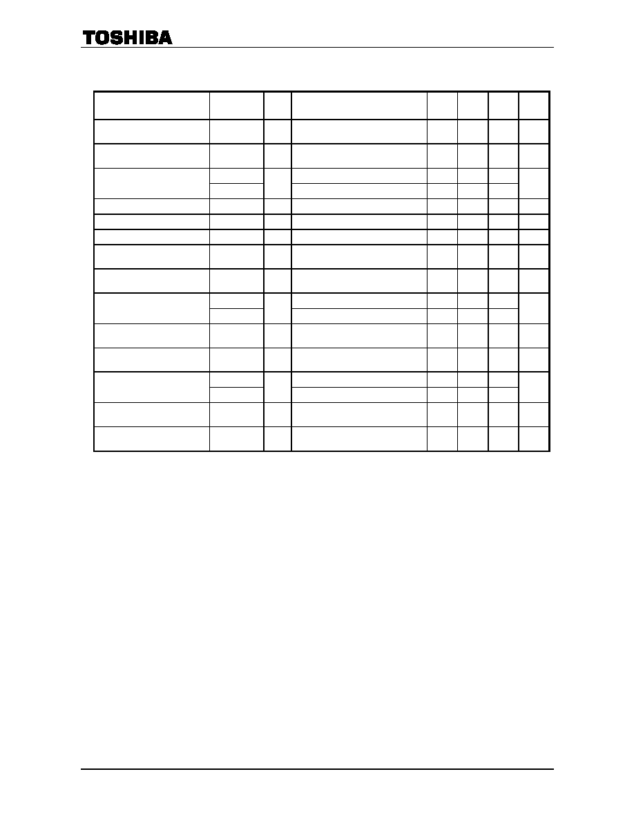
ELECTRICAL CHARACTERISTICS
(Unless otherwise stated, V
DD
= 5.0 V, V
CC
= 5.0 V, R
EXT
= 760 , Ta = -40~85�C)
CHARACTERISTIC SYMBOL
TEST
CIR-
CUIT
TEST CONDITION
MIN
TYP.
MAX
UNIT
I
CC1
1
SET NORMAL OPE. MODE, REXT
= 760 @OUT-a~Dp ALL ON, Ta
= 25�C
300
Operating Power Supply
Current for Output Block
I
CC2
1
SET NORMAL OPE. MODE, REXT
= 760 @OUT-a~Dp ALL ON V
CC
= 12 V, Ta = 25�C
320
mA
DIG-0 to DIG-3 Scan
Frequency
f
OSC
2
NORMAL OPE. MODE,
V
DD
= 4.5~5.5 V
240
480 960 Hz
OUT-a to Dp Output Sink
Current
I
SEG
3
NORMAL OPE. MODE,
V
CE
= 0.7 V, R
EXT
= 760
29 34 40 mA
DIG-0 to 3 Output Leakage
Current
I
leak1
4
ALL OFF MODE, V
CC
= 17 V
-20 �A
OUT-a to Dp Output Leakage
Current
I
leak2
4
ALL OFF MODE, V
CC
= 17 V
20 �A
DIG-0 to 3 Output Voltage
V
OUT
5
NORMAL OPE. MODE,
I
DIG
= -320 mA
3.0
V

TB62709NG/FG
2005-10-06
15
Logic block
CHARACTERISTIC SYMBOL
TEST
CIR-
CUIT
TEST CONDITION
MIN
TYP.
MAX
UNIT
I
DD1
6
STANDBY MODE, Ta = 25�C
200 �A
Static Power Supply Current for
Logic Circuits
I
DD2
6
BLANK MODE, Ta = 25�C
12.5 mA
Operating Power Supply
Current for Logic Circuits
I
DD3
6
NORMAL OPE. MODE,
f
CLK
= 10MHz,
DATA-IN : OUT-a~Dp = ON,
Ta = 25�C
20.5 mA
High Input Current for Logic
Circuits
I
IH
DATA-IN, LOAD & CLOCK :
V
IN
= 5 V
1 �A
Low Input Current for Logic
Circuits
I
IL
DATA-IN, LOAD & CLOCK :
V
IN
= 0 V
-1 �A
V
OH1
6
DATA-OUT, I
OH
= -1.0 mA
4.6
High Output Voltage for Logic
Circuits
V
OH2
6
DATA-OUT, I
OH
= -1.0 �A
V
DD
V
V
OL1
6
DATA-OUT, I
OL
= 1.0 mA
0.4
Low Output Voltage for Logic
Circuits
V
OL2
6
DATA-OUT, I
OH
= 1.0 �A
0.1
V
Clock Frequency
f
CLK
6
CASCADE CONNECTED,
Ta = -40~85�C
10
MHz
TB62709NG/FG
2005-10-06
16
SWITCHING CHARACTERISTICS
(Unless otherwise stated, V
DD
= 5.0 V, V
CC
= 5.0 V, Ta = 25�C)
CHARACTERISTIC SYMBOL
TEST
CIR-
CUIT
TEST CONDITION
MIN
TYP.
MAX
UNIT
Data Hold Time
(D-IN-CLOCK)
t
DHO
10 ns
Data Setup Time
(D-IN-CLOCK)
t
DST
20 ns
t
pHL-SO
C
L
= 10 pF
25
Serial Output Delay Time
(CLOCK-D-OUT)
t
pLH-SO
C
L
= 10 pF
25
ns
High Clock Pulse Width
t
CKH
30 ns
Low Clock Pulse Width
t
CKL
30 ns
Load Pulse Width
t
wLD
100 ns
Load Clock Time
(CLOCK-LOAD)
t
CLK-LD
50 ns
Clock Load Time
(LOAD-CLOCK)
t
LD-CLK
50 ns
t
pHL-SEG
C
L
= 10 pF
5.0
OUT-a to Dp Output Delay
Time (LOAD-OUTn)
t
pLH-SEG
C
L
= 10 pF
5.0
�s
OUT-a to Dp Output Rise Time
(OUTn)
t
r
SEG
C
L
= 10 pF
0.2
1.0
�s
OUT-a to Dp Output Fall Time
(OUTn)
t
f
SEG
C
L
= 10 pF
0.2
1.0
�s
t
pHL-DIG
C
L
= 10 pF
10.0
DIG-0~DIG-3 Output Delay
Time (LOAD-DIGn)
t
pLH-DIG
C
L
= 10 pF
10.0
�s
DIG-0~DIG-3 Output Rise
Time (DIGn)
t
r
DIG
C
L
= 10 pF
0.4
2.0
�s
DIG-0~DIG-3 Output Fall Time
(DIGn)
t
f
DIG
C
L
= 10 pF
0.4
2.0
�s

TB62709NG/FG
2005-10-06
17
RECOMMENDED OPERATING CONDITIONS
(Unless otherwise stated, V
DD
= 5.0 V, V
CC
= 5.0 V, Ta = -40~85�C)
CHARACTERISTIC SYMBOL
TEST
CIR-
CUIT
TEST CONDITION
MIN
TYP.
MAX
UNIT
Supply Voltage for Output Block
V
CC
4.0
6.0 V
DIG-0 to DIG-3 Output Source
Current
I
DIG
V
OUT
= 3.0 V
-320 mA
OUT-a to OUT-Dp Output Sink
Current
I
SEG
V
CE
= 0.7 V
40 mA
Logic block
CHARACTERISTIC SYMBOL
TEST
CIR-
CUIT
TEST CONDITION
MIN
TYP.
MAX
UNIT
Supply Voltage for Logic Block
V
DD
4.5
5.5 V
High Input Current for Logic
Circuits
I
IH
DATA-IN, LOAD & CLOCK,
V
IN
= V
DD
1 �A
Low Input Current for Logic
Circuits
I
IL
DATA-IN, LOAD & CLOCK,
V
IN
= 0V
-1 �A
High Input Voltage for Logic
Circuits
V
IH
0.7
V
DD
V
Low Input Voltage for Logic
Circuits
V
IL
0.3
V
DD
V
SWITCHING CONDITIONS
CHARACTERISTIC SYMBOL
TEST
CIR-
CUIT
TEST CONDITION
MIN
TYP.
MAX
UNIT
Data Hold Time
(D-IN-CLOCK)
t
DHO
30
ns
Data Setup Time
(D-IN-CLOCK)
t
DST
50
ns
Serial Output Delay Time
(CLOCK-D-OUT)
t
PDSO
C
L
= 10 pF
50
ns
High Clock Pulse Width
t
CKH
30
ns
Low Clock Pulse Width
t
CKL
30
ns
Load Pulse Width
t
wLD
150
ns
Load Clock Time
(CLOCK-LOAD)
t
CLKLD
100
ns
Clock Load Time
(LOAD-CLOCK)
t
LDCLK
100
ns

TB62709NG/FG
2005-10-06
18
TEST CIRCUITS
(1) I
CC1
, I
CC2
(2) f
OSC
TB62
709NG
/
FG
TB62
709NG
/
FG

TB62709NG/FG
2005-10-06
19
(3) I
SEG
(4) I
leak1
, I
leak2
TB62
709NG
/
FG
TB62
709NG
/
FG

TB62709NG/FG
2005-10-06
20
(5) V
OUT
(6) I
DD1
, I
DD2
, I
DD3
, V
OH1
, V
OH2
, V
OL1
, V
OL2
, f
CLK
TB62
709NG
/
FG
TB62
709NG
/
FG

TB62709NG/FG
2005-10-06
21
DUTY CYCLE SETTINGS AND OUTPUT CURRENT VALUES
Iout-Duty Cycle(TB62709NG)
Iout-Duty Cycle(TB62709FG)
Iout-Duty Cycle(TB62709NG)
Iout-Duty Cycle(TB62709FG)

TB62709NG/FG
2005-10-06
22
EXTERNAL RESISTANCE AND OUTPUT CURRENT VALUES
The following diagram shows application circuits.
Because operation may be unstable due to influences such as the electromagnetic induction of the wiring, the IC
should be located as close as possible to the LED.
The L-GND and P-GND of the IC are connected to the substrate in the IC.
Take care to avoid a potential difference exceeding 0.4V at two pins.
When executing the pattern layout, Toshiba recommends not including inductance components in the GND or
output pin lines, and not inserting capacitance components exceeding 50pF between the R
EXT
and GND.

TB62709NG/FG
2005-10-06
23
APPLICATION CIRCUIT EXAMPLE
(Connection example)
PRECAUTIONS for USING
Utmost care is necessary in the design of the output line, V
CC
(V
DD
) and (L-GND, P-GND) line since IC may be
destroyed due to short-circuit between outputs, air contamination fault, or fault by improper grounding.
TB62709NG
TB62709FG

TB62709NG/FG
2005-10-06
24
Package Dimensions
Weight: 1.62 g (typ.)

TB62709NG/FG
2005-10-06
25
Package Dimensions
Weight: 0.32 g (typ.)

TB62709NG/FG
2005-10-06
26