 | –≠–ª–µ–∫—Ç—Ä–æ–Ω–Ω—ã–π –∫–æ–º–ø–æ–Ω–µ–Ω—Ç: TB62731FU | –°–∫–∞—á–∞—Ç—å:  PDF PDF  ZIP ZIP |
TOSHIBA
TOSHIBA
TOSHIBA
TOSHIBA
TB62731FU
Available from:
Marktech Optoelectronics
120 Broadway ∑ Menands, NY 12203
800.984.5337 FAX: 518.432.7454
Website:
www.marktechopto.com
Email:
info@marktechopto.com
The information contained herein is subject to change without notice.
TOSHIBA BiCD INTEGRATED CIRCUIT SILICON MONOLITHIC
T B 6 2 7 3 1 F U
Step up DC-DC converter for LEDs
FEATURES
∑ The new driver incorporates a Pulse Current Drive Mode that raises
efficiency over 90% while driving up to six white LEDs in a serial
connection.
∑ In Direct Current Drive Mode white LEDs can be driven with very
low noise and efficiencies over 85%.
∑ The TB62731FU uses bi-cadmium (BiCD) process technology. This
new methodology allows for a reduction in the external component
count therefore lowering costs and improving battery life.
∑ Newly developed temperature derating technology predicts environmental temperature, including heat
dissipating from the driver IC itself, and adjusts current to optimize light emission.
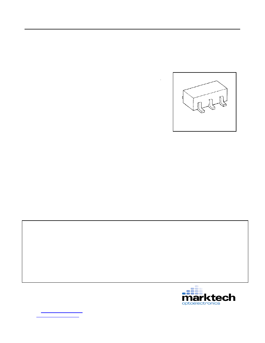
∑ Ultra compact 6-pin SOT23 package.
∑ Ability to drive all wavelengths and materials.
∑ +3.0V to +5.5V supply voltage
∑ Adjustable output current (Up to 320mW output power) 20mA driving current can be supply for LEDs with
16V total Vf
∑ Internal switching MOSFET (1.5 ohm typ)
∑
Shutdown function
SOT23 6pin
∑
TOSHIBA is continually working to improve the quality and reliability of its products. Nevertheless, semiconductor devices in general can malfunction or fail due to
their inherent electrical sensitivity and vulnerability to physical stress. It is the responsibility of the buyer, when utilizing TOSHIBA products, to comply with the
standards of safety in making a safe design for the entire system, and to avoid situations in which a malfunction or failure of such TOSHIBA products could cause
loss of human life, bodily injury or damage to property.
∑
In developing your designs, please ensure that TOSHIBA products are used within specified operating ranges as set forth in the most recent TOSHIBA products
specifications. Also, please keep in mind the precautions and conditions set forth in the "Handling Guide for Semiconductor Devices," or "TOSHIBA
Semiconductor Reliability Handbook" etc..
∑
The TOSHIBA products listed in this document are intended for usage in general electronics applications (computer, personal equipment, office equipment,
measuring equipment, industrial robotics, domestic appliances, etc.). These TOSHIBA products are neither intended nor warranted for usage in equipment that
requires extraordinarily high quality and/or reliability or a malfunction or failure of which may cause loss of human life or bodily injury ("Unintended Usage").
Unintended Usages include atomic energy control instruments, airplane or spaceship instruments, transportation instruments, traffic signal instruments,
combustion control instruments, medical instruments, all types of safety devices, etc. Unintended Usage of TOSHIBA products listed in this document shall be
made at the customer's own risk.
∑
The products described in this document are subject to the foreign exchange and foreign trade laws.
∑
The information contained herein is presented only as a guide for the applications of our products. No responsibility is assumed by TOSHIBA CORPORATION for
any infringements of intellectual property or other rights of the third parties, which may result from its use. No license is granted by implication or otherwise under
any intellectual property or other rights of TOSHIBA CORPORATION or others.

TOSHIBA
TOSHIBA
TOSHIBA
TOSHIBA
TB62731FU
Available from:
Marktech Optoelectronics
120 Broadway ∑ Menands, NY 12203
800.984.5337 FAX: 518.432.7454
Website:
www.marktechopto.com
Email:
info@marktechopto.com
The information contained herein is subject to change without notice.
Block Diagram
Pin Assignment
PIN
NO.
SYMBOL
FUNCTION
1
K
Feedback input pin.
Connect to the external LED driving current-sense resistor(R_sens).
2,5
GND
Ground pin
3
SHDN
Active "Low", shutdown control input pin.
TB72731FU falls into shutdown mode, when SHDN=L.
4
VCC
Supply voltage input pin.
Bypass this pin with a capacitor to ground as close to the device as possible.
6
A
Switching pin.
Inductor connection to the Drain of internal N channel MOSFET.
Both GND pins must be connected to external Ground.
K
A
V
CC
GND
SHDN
0.11V
OSC
R
Driver
S
Q
STB
REF
GND
R_lim
0.5 ohm
4
1
5
6
3
2
A
E

TOSHIBA
TOSHIBA
TOSHIBA
TOSHIBA
TB62731FU
Available from:
Marktech Optoelectronics
120 Broadway ∑ Menands, NY 12203
800.984.5337 FAX: 518.432.7454
Website:
www.marktechopto.com
Email:
info@marktechopto.com
The information contained herein is subject to change without notice.
Absolute Maximum Ratings (Ta = 25∞C)
PARAMETER
SYMBOL
RATING
UNIT
Power Supply Voltage
VCC
-0.3 ~ +6.0
V
Input Voltage
VIN
-0.3 ~ VCC+0.3V
V
Anode Current
I(A)
300
mA
Anode Voltage
V(A)
-0.3~+30
V
0.41
Power Dissipation
Pd
0.47
W
Rth(j-a)1 300
Saturated Thermal Resistance
Rth(j-a)1 260*
1
∞C/W
Operating Temperature Range
Topr
-40 ~ 85
∞C
Storage Temperature Range
Tstg
40 ~ +150
∞C
Junction Temperature
Tj
+125
∞C
<Note>
*1: Derate 3.8mW/∞C above +25∞C
Electrical Characteristics
(V
CC
=3.0V~5.5V, Ta = +25∞C, unless otherwise specified.)
PARAMETER SYMBOL
TEST
CONDITION
MIN.
TYP.
MAX.
UNIT
Supply Voltage
VCC
3.0
5.5
V
Supply Current
ICC(ON)
VCC=3.6V
600
900
uA
Quiescent Current
ICC(SHDN)
SHDN=GND
0.5
uA
SHDN Input Current
I_SHDN
SHDN=VCC
4.2
7
uA
Internal MOSFET
ON-Resistance
Ron
I(A)=220mA or less,
including R_lim
2.0
2.5
ohm
Anode Voltage
V(A)
30
V
Anode
Current
I(A)
220 mA
Anode Leak Current
IOZ(A)
SHDN=GND
0.5
1
uA
LED Current (average)
Io(K)
R_sens=1.8 ohm
18*
1
20*
1
22*
1
mA
Derating Function
Start Temperature
Tder
Io(K)=20mA,
Ta=25
∞C
(45)*
2
∞C
<Note>
*1: See figure of "LED current vs. Feedback resistance"
*2: The specification in parenthesis is not tested. For design purpose, current derating should
be considered to start at Tj=45∞C.

TOSHIBA
TOSHIBA
TOSHIBA
TOSHIBA
TB62731FU
Available from:
Marktech Optoelectronics
120 Broadway ∑ Menands, NY 12203
800.984.5337 FAX: 518.432.7454
Website:
www.marktechopto.com
Email:
info@marktechopto.com
The information contained herein is subject to change without notice.
Typical Performance Characteristics
S u p p ly C u rre n t v s . S u p p ly V o lta g e
(N o rm a l O p e ra tio n )
4 0 0
5 0 0
6 0 0
7 0 0
8 0 0
9 0 0
3
3 .5
4
4 .5
5
5 .5
V C C ( V )
ICC(ON) (uA)
S up p ly C urre nt vs . S up p ly V o lta g e
(S hutd o w n M o d e )
0
0 .1
0 .2
0 .3
0 .4
0 .5
3
3 .5
4
4 .5
5
5 .5
V C C (V )
ICC(SHDN) (uA
)
Switching Frequency vs. Supply Voltage
300
320
340
360
380
400
3
3.5
4
4.5
5
5.5
VCC (V)
Fs (kHz)
TB62731FU
VCC
1
2
3
4
5
6
TB62731FU
VCC
1
2
3
4
5
6
TB62731FU
VCC
1
2
3
4
5
6
To Monitor

TOSHIBA
TOSHIBA
TOSHIBA
TOSHIBA
TB62731FU
Available from:
Marktech Optoelectronics
120 Broadway ∑ Menands, NY 12203
800.984.5337 FAX: 518.432.7454
Website:
www.marktechopto.com
Email:
info@marktechopto.com
The information contained herein is subject to change without notice.
Operational Description
TB62731FU is a pulse-skipping converter that uses a combined control scheme of voltage feedback
loop and current limited feedback loop to operate constant LED driving current. Operation can be easily
understood by referring to the Block Diagram and Switching Waveforms.
The internal MOSFET is turned on when amplifier A senses that the average voltage at R_sens is lower
than REF level. The N-channel MOSFET stays "turned on" until either the switching current peak
reaches 220mA(typ), or the oscillator automatically turns it off at its maximum on-duty (83.3%). Once
turned off, the MOSFET keeps off during the off-time. Subsequently, if the R_sens voltage is still lower
than reference level, another switching cycle is started. Otherwise, the internal MOSFET remains turned
off as long as the average R_sens voltage is higher than reference level.
[Shutdown Mode]
The TB62731FU falls into shutdown mode, when SHDN="L". In shutdown mode, the reference, control
circuitry, oscillator and internal switching MOSFET are stopped and current consumption is reduced
below 0.5uA. Connect SHDN to "VCC" for normal operation.
Switching Waveforms Illustration
V(A)
OSC
Inductor
current
I(A)
LED
current
Fs=360 kHz
on-duty(max)=83.3%
220 mA
Average
Current
Preset LED current level

TOSHIBA
TOSHIBA
TOSHIBA
TOSHIBA
TB62731FU
Available from:
Marktech Optoelectronics
120 Broadway ∑ Menands, NY 12203
800.984.5337 FAX: 518.432.7454
Website:
www.marktechopto.com
Email:
info@marktechopto.com
The information contained herein is subject to change without notice.
[Driving Current Derating Function]
In order to avoid application problems, it is important to stay within the LED Lamps maximum ratings.
This is especially critical when determining the maximum allowable driving current, which needs to be
derated depending on atmospheric temperature. The TB62731FU has a built-in current derating
function that helps light LED lamps safely and efficiently.
TB62731FU's driving current derating function is designed to start working at 45∞C in Tj as shown in
Figure 1. When the driving current is 20mA, derating is expected to start approximately at 25∞C in Ta.
The difference between Tj and Ta depends on LED driving current, IC mounting conditions, PCB
patterns, cooling conditions. The initial driving current level must be set carefully so as not to exceed the
absolute maximum ratings of LEDs.
With Toshiba's original derating function the TB62731FU can supply a higher LED driving current thus
eliminating current limitations in high temperatures. Competitive ICs do not have this function, therefore
this feature will contribute to a reduction in the amount of LED lamps used.
FIGURE 1
Solid line; Tj operation, Dotted line; Ta operation
Current Derating Function
0
5
10
15
20
25
0
20
40
60
80
Temperature Tj / Ta (∞C)
LED Driving Current (mA
)

TOSHIBA
TOSHIBA
TOSHIBA
TOSHIBA
TB62731FU
Available from:
Marktech Optoelectronics
120 Broadway ∑ Menands, NY 12203
800.984.5337 FAX: 518.432.7454
Website:
www.marktechopto.com
Email:
info@marktechopto.com
The information contained herein is subject to change without notice.
Application Information
[Typical Application Circuit]
Efficiency data are taken under the following conditions;
Loads
four white LED lamps
Inductor 47uH
Schottky Diode
Vf=0.35V@0.7A
Io(K)=20mA (R_sens=1.8 ohm), Ta; 25 ∞C
E fficie ncy vs . S up p ly V o lta g e
6 0
7 0
8 0
9 0
1 0 0
3
3 .5
4
4 .5
5
5 .5
V C C (V )
Efficiency (%)
K
A
VCC
VIN = 3V 5.5V
TB62731FU
SHDN
R_sens
Inductor Schottky
Diode
White LED
GND
Cin
1uF
Cout
1uF
ON
OFF
GND

TOSHIBA
TOSHIBA
TOSHIBA
TOSHIBA
TB62731FU
Available from:
Marktech Optoelectronics
120 Broadway ∑ Menands, NY 12203
800.984.5337 FAX: 518.432.7454
Website:
www.marktechopto.com
Email:
info@marktechopto.com
The information contained herein is subject to change without notice.
[Important Notice]
In a Typical Application Circuit, the total Vf of LED lamps must be kept larger than VCC. As the external
inductor, Schottky diode, LED lamps and R_sens are connected in a series, if the total Vf is below VCC,
very high currents are likely to surge into the LED lamps.
[Setting LED Driving Current]
TB62731FU is a constant output current DC/DC converter. R_sens sets the average LED driving current.
(See LED driving current, Total Vf vs. Feedback resistor in this section). Also maximum supply power is
limited by the following equation:
Io(K) x Total Vf(max) 320mW
Where Io(K) is the average LED current. Therefore, 20mA driving current can be supplied for LEDs with
the total Vf(max) of 16V and this current is given by R_sens of 1.8ohm. Note that Io(K) x Total Vf(max)
over 320mW makes output voltage smaller than Total Vf(max) and turns the LED lamps off.
[Output Capacitor Selection]
The LED current ripple level deeply depends on the output buffering capacitor value. Larger values help
to reduce output ripple and noise. TB62731FU, however, monitors the average voltage at R_sens,
therefore low ripple driving current, like a DC current, is not necessarily needed. The capacitor value is
not critical as viewed from LED current controlability. The output capacitance value will be decided by
peak level of LED current and noise.
LED driving current, total Vf
vs. Feedback resistor
0
5
10
15
20
25
30
35
40
0.5
1
1.5
2
2.5
3
R_sens (ohm)
Io(K) (mA)
8
12
16
20
24
total Vf(max.) (V
)
<
=

TOSHIBA
TOSHIBA
TOSHIBA
TOSHIBA
TB62731FU
Available from:
Marktech Optoelectronics
120 Broadway ∑ Menands, NY 12203
800.984.5337 FAX: 518.432.7454
Website:
www.marktechopto.com
Email:
info@marktechopto.com
The information contained herein is subject to change without notice.
[Inductor Selection]
A recommended inductance value is 47uH, however, values from 33uH to 56uH can also be acceptable.
Low DC resistance inductors are preferable for minimizing power losses.
[PCB Pattern Layout]
When designing PCB patterns, minimize trace lengths to the inductor, pin A, Schottky diode and
buffering capacitors. Also, as for feedback traces, keep them short and away from noisy traces, like an
inductor's trace. Both buffering capacitors should be placed as close to the IC as possible.
Package Dimension
(Unit: mm)
Marking
Top View
1 6
2 5
3 4
0~0.1
1.1
+0.2
- 0.1
0.16
+0.1
- 0.06
1
2
3
2.8
6
5
4
+0.2
- 0.3
1.6
+0.2
- 0.1
0.3
+0.1
1.9
+0.2
0.95
0.95
2.9
+0.2
-
-
-