
TOSHIBA BiCD DIGITAL INTEGRATED CIRCUIT SILICON MONOLITHIC
T B 6 2 7 3 2 F U
TOSHIBA
T B 6 2 7 3 2 F U
FEATURE
The TB62732FU is a LED driver by the high efficiency
step up type DC-DC converter that 2-4 serial white LED
can be turned on.
This IC builds in the NchMOS FET transistor to switch
the coil, and builds in the function which derate
the LED current corresponding to the rise in temperature.
And, the average LED current can be set up easily
by the resistance with the outside.
This IC is the most suitable as a driver
of the LED liquid crysta back light of the PDA,
the cellular phone and the the handy terminal.
CHARACTERISTICS
*Maximum output voltage Vo =< 17V
*The variable setup of the average LED current value by
the resistance with the outside.
18 mA (typ) @ R_sens = 2.7 ohms
20 mA (typ) @ R_sens = 2.4 ohms
*Supply electric power
It is turned on to the 320 mW load.
*Compact package
SSOP6 - P - 0.95B ( SOT23-6pin )
*The LED current derating function is built in.
The derating of LED current vs set temperature,
on the automatic operation.
*High efficiency
80% of the efficiency. @ 2-3LEDs turn on. IF=20mA (typ) )
Ron=2.0 ohms (standard) @ Vin = 3.0 - 5.5V
The power MOS transistor building in of low Ron.
*Pin assignment (Top View)
Note 1:
Be careful of handling because there is a terminal which is poor at ESD in this product.
The step up type DC-DC converter only for white LED driver lighting
Weight: 0.016 g (typ)
T B 6 2 7 3 2 F U
SSOP6-P-0.95B
K
GND
SHDN
A
GND
VCC
V
Company Headquarters
3 Northway Lane North
Latham, New York 12110
Toll Free: 800.984.5337
Fax:
518.785.4725
Web: www.marktechopto.com | Email: info@marktechopto.com
California Sales Office:
950 South Coast Drive, Suite 265
Costa Mesa, California 92626
Toll Free: 800.984.5337
Fax: 714.850.9314
Company Headquarters
3 Northway Lane North
Latham, New York 12110
Toll Free: 800.984.5337
Fax:
518.785.4725
Web: www.marktechopto.com | Email: info@marktechopto.com
California Sales Office:
950 South Coast Drive, Suite 265
Costa Mesa, California 92626
Toll Free: 800.984.5337
Fax: 714.850.9314

TOSHIBA
T B 6 2 7 3 2 F U
27, Feb 2002 (Ver.04)
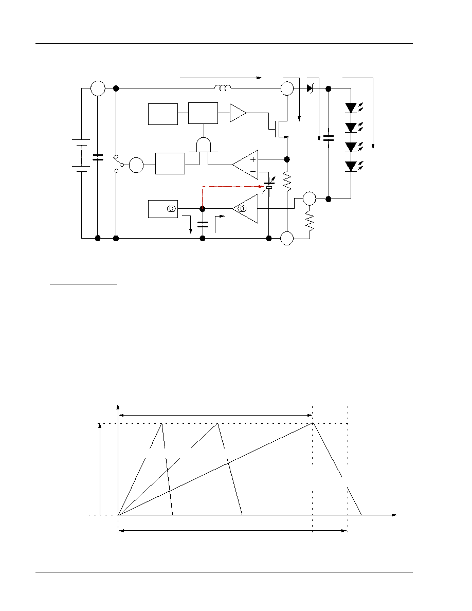
BLOCK DIAGRAM
No
Name
Function explanation
1
K
It is the connection terminal with cathode and IF setup resistance of
LED. It is the feedback terminal of the charge voltage wave form for the
LED current control.
2, 5
GND
It is the ground terminal of the logic part.
3
SHDN
It is the enable terminal. It becomes the standby mode with "L", and the
LED is turned off. The lighting operation is given with "H".
4
Vcc
It is the input terminal of the operation voltage for the IC. The operating
voltage is 3.0 to 5.5V.
6
A
It is the switch terminal of the coil for the DC/DC converter. The switch is
a Nch MOSFET transistor. This is low Ron.
2
FIg 1 : BLOCK DIAGRAM
TERMINAL EXPLANATION
Note 2 : Connect all the GND terminals to the ground electric potencial.
K
0 - 0.12V
OSC
R
S
Q
STB
A
i(sub)
i(add)
1.0MHz
Vcc
GND
SHDN
A
0.35
GND
REF
Buffer

TOSHIBA
T B 6 2 7 3 2 F U
27, Feb 2002 (Ver.04)
Characteristics
Symbol
Rating
Unit
Supply voltage
Vcc
- 0.3 to + 6.0
V
Input voltage
Vin
- 0.3 to VCC + 0.3
A(anode) terminal
current
Io(A)
+ 380
mA
A(anode) terminal
voltage
Vo(A)
- 0.3 to + 17
V
Power dissipation
Pd
0.41 ( not on PCB )
W
0.47 (on PCB) *Note 3
Saturation heat
resistance
Rth(j-a)1
300 ( not on PCB )
degree/W
Rth(j-a)2
260 ( onPCB )
Operation
temperature
Topr
- 40 to + 85
Storage
temperature
Tstg
- 40 to + 150
degree
Maximum juction
temperature
Tj
125
Note 3 : When every time the ambient temperature gets over 25 degrees with 1 degree, the
allowable loss must reduce 3.8mW/degree more than maximum rated value. ( When on PCB.)
ABSOLUTE MAXIMUM RATING ( unless otherwised notice Topr = 25 degree )
Characeristics
Symbol
Test condition
min
typ
max
Unit
Supply voltage
Vcc
-
3.0
-
4.3
V
SHDN terminal
H-level input
voltage
VIH
-
Vcc
-0.5
-
Vcc
V
SHDN terminal
L-level input voltage
VIL
-
0
-
0.5
SHDN terminal
"H"level input pulse
width
tpw SHDN
-
0.5
-
-
ms
Setup LED current
(mean)
Io
Maximum step up condition.
Vo (A) is change from 3V to
16V
5
-
20
mA
RECOMMENDED OPERATION CONDITION (unless otherwise notice Topr = -40 to 85 degree)
3

TOSHIBA
T B 6 2 7 3 2 F U
27, Feb 2002 (Ver.04)
Characteristics
Symbol
Test condition
min
typ
max
Unit
Supply voltage
Vcc
3.0
-
5.5
V
Operation supply
current
Icc(On)
Vcc = 3.6V
-
0.9
mA
Stand-by supply
current
Icc(SHDN)
SHDN = 0 V
-
0.5
1.2
uA
SHDN terminal
current
I_SHDN
SHDN = Vcc,
built in pull-down resisance
-
4.2
7
uA
MOS-Tr on
resistance
Ron
Io(A) <= 380 mA,
detection resistance value is
contained.
-
2.0
2.5
ohms
MOS-Tr switching
frequency
fOSC
0.7
1.0
1.3
MHz
A terminal voltage
Vo(A)
17
-
-
V
A terminal current
Io(A)
320
350
380
mA
A terminal
leakage current
Ioz(A)
-
0.5
1
uA
Set up LED
current (mean)
Io
Vcc = 3 - 4.3V,
R_sens = 2.7 ohms,
19.6
mA
LED current Vcc
dependence
dIo
L = 6.8uH,
Topr = 25 degree (Note 4)
+/-5
+/-10
%
Derating start
ambient
temperature
Tdel
R_sens = 2.7 ohms, L = 10uH,
Vo = 16V (Note 5)
-
45
-
degr
ee
ELECTRIC CHARACTERISTICS
( unless otherwised notice, Topr = -40 to 85 degree & Vcc = 3.0 to 5.5 V)
Note 4 : The derating function carries out the measurement in Ta= 25 degree not to work. The
specifications don't contain the dispersion of the R_Sens resistor. Io has the possibility to be different
from the specifications by the inductance value and the relations of the load.
Note 5 : It is a specifications guarantee by the design.
4
TOSHIBA
T B 6 2 7 3 2 F U
27, Feb 2002 (Ver.04)
BASIC OPERATION
The step up type DC/DC converter is applied, and the basic circuit of the TB62732FU adopts peak control of
the current pulse.
The internal MOS transistor NMOS is turned on in the fixed frequency fOSC =1MHz, and the charge has the
energy in the inductance.
Inductance electric current IL turns off NMOS when it reaches 80% of 1/1MHz when it
increased from IL = 0 and it reached IL = ILpeak = 380 (mA, typ).
The shot key diode is turned on, and IL = Ic2 flows, because the coil may keep IL = ILpeak.
After that, Ic2 is decrease, and become IL = 0.
This operation is repeated, and Ic2 is fully done as to the charge, and it becomes Io, and flows to LED.
The details of a basic pulse to use for the current control are shown in Fig 3.
5
T = 1/fOSC, fOSC = 1MHz(typ)
Muximum duty 80 %
ILpeak=
380(mA, max)
When fitness inductance
IL = IL peak
When Un-fitness inductance
Fig 3 : the switching wave form of the inductance
Fig 2 : the application circuit (example)
K
A
GND
0 - 0.12V
OSC
Buffer
R
S
Q
REF
A
0.35
i(sub)
i(add)
1.0 MHz
R_sens
IL, ILpeak
Io
Ic2
NMOS
C2
6.8 uH
Vcc
C1
SHDN
Vin
STB
IL becomes 0 in the time.
IL doesn't become 0 in the time.

TOSHIBA
T B 6 2 7 3 2 F U
27, Feb 2002 (Ver.04)
6
Fig 4 : burst control wave form
THE STAE OF THE PEAK CURRENT CONTROL
The peak current control is repeat in the control the waveform which showed it in the Fig 3.
The current pulse of the Fig 3 is a charging current on the output capacitor C2.
It is supplied to LED as a discharge current on the output side capacitor, and it through the R_sens to GND.
And, as for the charging voltage waveform of the output capacitor C2, it returns in the IC from the K terminal.
The internal circuit which the K terminal should be input from controls the current pulses so that the
average voltage value of the voltage wave form which it could get may become 53 mV (typ).
The constant current is controlled as a result as an average electric current value. Therefore, when R_sens = 2.7
ohm is connected, the average current value of (53 mV /2.7 ohms) = 19.6 mA can get it.
This IC is designed for the purpose of supplying the power 320 mW (min).
Generally it is a step up inductance 6.8 uH to the load power 320 mW. And, when the load electric power is small, it
can be done small for the inductance.
As a condition about the LED load between the generator terminal and the K terminal,
Please keep the condition in Vin (Vcc) < LED VF total.
There are no relations with the control of the IC, and LED is always turned on.
STANDBY MODE OPERATION
The SHDN terminal set-up the normal operation and the standby operation. The lighting operation is possible in
the "L" level in the stop (at the standby mode), the "H" level. Still, consumption supply current in the standby mode
is 1.2uA (max).
A-terminal voltage
A-terminal current
(External inductor current)
K-terminal voltage
(Waveform of current for cap. charge)
Maximum On pulse
width = 85%
I A( peak )
LED Vf
Switching frequency fOSC = 1MHz
It stabilizes it in the set Io
with lowering IA (peak).
It stabilizes it in the set Io
with lowering IA (peak).

TOSHIBA
T B 6 2 7 3 2 F U
27, Feb 2002 (Ver.04)
7
THE SETUP ON THE OUTPUT SIDE CAPACITOR
The C2 is upper 0.47(uF) above is recommended from the consideration to the IF peak.
THE SETUP ON THE INDUCTANCE
The minimum inductance with the outside is calculated with the next formula.
L(uH) = ((K*Po)-Vin min.*Io)*(1/fOSC min.)*2*(1/(Ip min.*Ip min.)) - - - Form 2
Each clause is as mentioned in the following.
Po (W) : output power (the electric energy which should be necessary the LED load)
Po (W) = (VF LED*IF LED)+(Vf schottky*IF LED)+(R_sens*IF LED*IF LED)
( Forward current of LED is IF LED (mA) = Setup currnet Io (mA), Forward voltage of LED is VF LED (V),
Forward voltage of schottky diode is VF schottky (V), Setup resistance of output currnet is R_sens (ohms) )
Vin min (V) : Minimum input voltage(battely voltage)
When there is a resistance element on the input voltage side, that one for the voltage descent is taken into
consideration to the minimum input voltage.
The input Iin is estimated roughly in Form 3.
Iin (mA) = Vo / Vin * IF --- Form 3
Example, the voltage drop of 1(V) occurs when it becomes Iin = 0.1(A) and has the line resistance of
1 (ohms).
At this time, Vin=3.1 (V) becomes minimum Vin value because the minimum Vcc specifications of spec
is Vcc=3.0 (V).
Io (A) : The average current value established with R_sens. Show the fig-5 on next page.
fOSC(Hz) : The switching frequency of the internal MOS transistor.
The specification of fOSC(MHz) = 0.7 min, 1.0 typ and 1.3 max.
Ip (A) : Peak current value to supply to the inductance.
The specification of Ip (mA) = 320 min, 350 typ, 380 max.
For example, the following condition is substituted for the formula.
It is supposed under condition.
Input voltage Vin : Vin=3.0-4.3(V),
Output side capacitance C2 : C2=0.47(uF) - - - C2 is ignored by the calculation.
VF LED = 16(V), schottly diode VF: Vf schottky = 0.3(V),
Setup resistence R_sens : R_sens = 2.7(ohms), Setup current Io : Io = 19.6(mA).
L (uH) = ((16*0.0196+0.3*0.0196+2.7*0.0196*0.0196)-Vin*0.0196)*(1/700e3)*2*(1/(0.32*0.32))
= 7.19(uH, Vin = 3.0V) and 6.59 (uH,Vin = 4.3V)
Therefore, 7.19(uH) in Vcc=3.0V whose input voltage is low is chosen.
It is sufficient by the above calculation on the standard condition.
If the worst case is taken into consideration, the coil of about 1.1 times of the calculation is chosen.
L(uH)=7.19(uH)*1.1 >= 7.90 (uH)
Capacitor C2 (uF)
Ripple current (mA)
Note
0.01
15-25
0.1
5-8
0.47
2-4
Recommend
1
1-3

TOSHIBA
T B 6 2 7 3 2 F U
27, Feb 2002 (Ver.04)
1
10
1.2
1.5
1.8
2
2.2
2.7
3.3
4.7
5.6
6.8
8.2
9.1
Setup resistance R_sens(ohm)
0
5
10
15
20
25
30
35
Setup current ,ho(mA)
4LEDs
add 3LEDs range
add 2LEDs range
Setup current Io vs Setup resistance R_sens
(Typical value. Vcc=3.6V Ta = 25 degree)
CHOICE OF THE R_sens
The resistance R_sens (ohm) in the K terminal - GND is of the outout current Io for the setup.
The average outout current Io(mA) can be set up by a resistance value.
Average setup electric current Io (mA) is estimated roughly in the following.
Io (mA) = 53(mV) / R_sens (ohm)
For example, R_sens = 2.7 (ohm) becomes Io = 19.6 (mA).
The absolute value accuracy of the current is to take the +/-12 percent into consideration.
(The accuracy of R_sens isn't contained.)
When 320 (mW) is output, this IC recommends L=10 (uH).
Example, when the output power gets over 320 (mW), the setup current Io has the possibility that Io
doesn't meet the set point.
And, this IC can get the setup current Io even if the output side capacitor C2 isn't connected.
In this case, be careful in the rush current IFP (mA) to LED because the LED current becomes the pulse
current of the maximum peak magnitude 380 (mA).
Shortening circuit board wiring by using the part whose reactance element is small as much as possible is
recommended with the R_sens resistor.
And, mounting it near here as much as possible is recommended with each part in application circuit
as well.
8
Fig 5 : The graph of the setup current Io and the setup resistance R_sens

TOSHIBA
T B 6 2 7 3 2 F U
27, Feb 2002 (Ver.04)
9
ABOUT THE CURRENT DERATING FUNCTION
As for the LED current, generally the current derating recommended against the rise in the ambient temperature.
The TB62732FU aims at turning on white LED of the back light illuminant of the color LCD safely and efficiently,
and builds in the current derating function which set temperature was presumed.
This IC has the character which makes the current 100(%) in the case of Tjs=45 (degree) and which makes
the current 0(%) again in the case of Tjs=100 (degree) corresponding to internal detection temperature Tjs.
When it is seen from set temperature Ta (degree), the temperature that self-fever temperature Tup (degree)
in the operation was reduced from Tjs = 45 (degree) becomes a starting temperature Ts (degree).
Starting temperature Ts (degree) = 45 (degree) - self-fever temperature Tup (degree) --- Form 4
Therefore, the derating character functions as the figure 6, and shows internal detection temperature Tjs and
the rate of change of the outout current.
Self-fever temperature Tup (degree) in the operation is calculated with the Form 5.
Self-fever temperature Tup (degree) ---- ceremony 5
= (P loss (W) - P parts(W))*Rth(j-a) (degree/W)
It is described in the following about each clause.
DC resistance of the inductance : RDC(ohm), Forward current of LED : IF LED(A),
Total forward voltage of LED : VF LED(V), Forward voltage : VF schottky(V),
Setup resistance : R_sens(ohm), Power loss of lighting circuit : P loss(W)=(Po/efficiency)-Po(W),
Power loss of parts : P parts(W)=RDC*Iin+VF schottky*IF LED+R_sens*IF LED*IF LED,
Saturation thermal resistance of package :
Rth(j-a) (degree/W) =< 260 - - - when on board, muximum
Output power :
Po(W) = VF LED*Io(A)
Input power :
Pi(W) = Vin (V)*Iin(A)
Efficiency :
Efficiency(%)=100*(Po/Pi)
Example : When the measurement of the lighting circuit tightened each following value.
RDC=0.5(ohm), Po=320(mW), Iin=0.1(A), Io=20(mA), R_sens=1.8(ohm), VF schottky=0.3(V),
Efficiency=70(%)
In this case, self-fever temperature Tup
Tup (degree)= ((0.32-(0.32*0.7))-(0.5*0.1+0.3*0.0196+2.7*0.0196*0.0196))*260 =10.16 (degree)
Start temperatue Ts(degree)=45(degree)-10.16(degree)=33.4(degree)
Io is controlled as the Fig 6 as a result within the recommendation current area of LED.
The saturation thermal resistance Rth(j-a) = 260 (degree /W) is maximum value. They sometimes become
the Rth(j-a) = 210 - 260 (degree /W) by mounting.
And, the individual difference is formed in the starting temperature with the character of the IC and the influence
of the difference in the environment of the use.
Fig 6 : the derating function of the setup current
0
25
50
75
100
Ts/Tjs (degree)
0
20
40
60
80
100
120
Rate of the Outout Current.
The change of
Ts=34.4(degree)
(20mA=100%)
The
recommendation
current area of LED
(25mA conversion)
The change by Tjs

TOSHIBA
T B 6 2 7 3 2 F U
27, Feb 2002 (Ver.04)
Supply current in the operation ICC (on)
3
3.5
4
4.5
5
5.5
Vcc (V)
0
100
200
300
400
500
600
700
800
900
Supply current (uA)
4
3
1
2
5
6
TB62732FU
Vcc
Suppy current in the shut-down mode Icc(SHDN)
3
3.5
4
4.5
5
5.5
Vcc (V)
0
0.1
0.2
0.3
0.4
0.5
Supply current (uA)
4
3
1
2
5
6
TB62732FU
Vcc
4
3
1
2
5
6
TB62732FU
Vcc
Switching frequency of inductanse
3
3.5
4
4.5
5
5.5
Vcc (V)
300
320
340
360
380
400
Switching frequency
fOSC
10

TOSHIBA
T B 6 2 7 3 2 F U
27, Feb 2002 (Ver.04)
Application evaluation circuit example 1
(The evaluation result example by the small coil. : Coil = LDR304612T-6R8)
6.8uH is the most suitable when serial 3-4LED are turned on by IF= 20m A.
4.7uH is recommended when serial 2LED is turned on steadily in the range of VIN>4.5V.
11
3
3.2
3.4
3.6
3.8
4
4.2
Vin (V)
15
20
25
LED Current IF (mA)
65
70
75
80
85
Efficiency (%)
4LED Efficiency
4LED IF
Vin - Efficiency/IF
3
3.2
3.4
3.6
3.8
4
4.2
Vin (V)
15
20
25
LED Current IF (mA)
65
70
75
80
85
Efficiency (%)
3LED Efficiency
3LED IF
Vin - Efficiency/IF
3
3.2
3.4
3.6
3.8
4
4.2
Vin (V)
15
20
25
LED Current IF (mA)
65
70
75
80
85
Efficiency (%)
2LED Efficiency
2LED IF
Vin - Efficiency/IF
L1
6.8uH
S-Di
VIN
3.2-4.2V
C1
2.2uF
C2
0
.
47
uF
ON
OFF
R_SENS
2.6
L1:
TDK LDR304612T-6R8
S-Di: TOSHIBA
1SS404
20V/1A
LED:
NICHIA NSCW215T
2-4LEDs
0.01uF
K
A
VCC
SHDN
GND
GND
Efficiency
(%)
Ave Efficiency(%)
2LED
79.0-83.8
81.6
3LED
75.1-80.9
78.3
4LED
72.0-78.3
75.7
IF (mA)
Vcc dependence
(%)
2LED
19.5-21.1
7.8
3LED
19.5-20.5
4.9
4LED
19.6-20.7
5.3
The efficiency of the VIN=3.0-4.3V range
The IF of the VIN=3.0-4.3V range
<Measurement>
Note : The value is our company actual measurement value.
The result has the possibility to be different by the measurement
environment.

TOSHIBA
T B 6 2 7 3 2 F U
27, Feb 2002 (Ver.04)
Application evaluation circuit example 2
(The evaluation result example by the small coil. : Coil = CXML321610-7R0)
6.8uH is the most suitable when serial 3-4LED are turned on by IF= 20m A.
4.7uH is recommended when serial 2LED is turned on steadily in the range of VIN>4.5V.
12
3
3.2
3.4
3.6
3.8
4
4.2
Vin (V)
15
20
25
LED Current IF (mA)
65
70
75
80
85
Efficiency (%)
4LED Efficiency
4LED IF
Vin - Efficiency/IF
3
3.2
3.4
3.6
3.8
4
4.2
Vin (V)
15
20
25
LED Current IF (mA)
65
70
75
80
85
Efficiency (%)
3LED Efficiency
3LED IF
Vin - Efficiency/IF
3
3.2
3.4
3.6
3.8
4
4.2
Vin (V)
15
20
25
LED Current IF (mA)
65
70
75
80
85
Efficiency (%)
2LED Efficiency
2LED IF
Vin - Efficiency/IF
L1
6.8uH
S-Di
VIN
3.2-4.2V
C1
2.2uF
C2
0
.
47
uF
ON
OFF
R_SENS
2.6
L1:
SUMITOMO CXML321610-7R0
S-Di:
TOSHIBA 1SS404 20V/1A
LED:
NICHIA NSCW215T
2-4LEDs
0.01uF
K
A
VCC
SHDN
GND
GND
Efficiency
(%)
Ave Efficiency(%)
2LED
78.2-84.1
81.3
3LED
72.0-79.1
75.8
4LED
66.9-71.1
74.6
IF (mA)
Vcc dependence
(%)
2LED
19.8-21.6
8.1
3LED
20.0-21.0
4.8
4LED
20.4-21.5
4.9
The efficiency of the VIN=3.0-4.3V range
The IF of the VIN=3.0-4.3V range
<Measurement>
Note : The value is our company actual measurement value.
The result has the possibility to be different by the measurement
environment.

TOSHIBA
T B 6 2 7 3 2 F U
27, Feb 2002 (Ver.04)
Application evaluation circuit example 3
(The evaluation result example by the small coil. : Coil = 976AS-6R8)
6.8uH is the most suitable when serial 3-4LED are turned on by IF= 20m A.
4.7uH is recommended when serial 2LED is turned on steadily in the range of VIN>4.5V.
13
3
3.2
3.4
3.6
3.8
4
4.2
Vin (V)
15
20
25
LED Current IF (mA)
65
70
75
80
85
Efficiency (%)
4LED Efficiency
4LED IF
Vin - Efficiency/IF
3
3.2
3.4
3.6
3.8
4
4.2
Vin (V)
15
20
25
LED Current IF (mA)
65
70
75
80
85
Efficiency (%)
3LED Efficiency
3LED IF
Vin - Efficiency/IF
3
3.2
3.4
3.6
3.8
4
4.2
Vin (V)
15
20
25
LED Current IF (mA)
65
70
75
80
85
Efficiency (%)
2LED Efficiency
2LED IF
Vin - Efficiency/IF
L1
6.8uH
S-Di
VIN
3.2-4.2V
C1
2.2uF
C2
0
.
47u
F
ON
OFF
R_SENS
2.6
L1:
TOKO 976AS-6R8
S-Di: TOSHIBA
1SS404
20V/1A
LED:
NICHIA NSCW215T
2-4LEDs
0.01uF
K
A
VCC
SHDN
GND
GND
Efficiency
(%)
Ave Efficiency(%)
2LED
79.7-84.4
82.3
3LED
76.7-82.1
79.5
4LED
73.1-79.7
74.0
IF (mA)
Vcc dependence
(%)
2LED
19.4-21.1
8.1
3LED
19.5-20.5
5.1
4LED
19.6-20.7
5.3
The efficiency of the VIN=3.0-4.3V range
The IF of the VIN=3.0-4.3V range
<Measurement>
Note : The value is our company actual measurement value.
The result has the possibility to be different by the measurement
environment.

TOSHIBA
T B 6 2 7 3 2 F U
27, Feb 2002 (Ver.04)
Application evaluation circuit example 4
(The evaluation result example by the small coil. : Coil = CXLD140-6R8)
6.8uH is the most suitable when serial 3-4LED are turned on by IF= 20m A.
4.7uH is recommended when serial 2LED is turned on steadily in the range of VIN>4.5V.
14
3
3.2
3.4
3.6
3.8
4
4.2
Vin (V)
15
20
25
LED Current IF (mA)
65
70
75
80
85
Efficiency (%)
4LED Efficiency
4LED IF
Vin - Efficiency/IF
3
3.2
3.4
3.6
3.8
4
4.2
Vin (V)
15
20
25
LED Current IF (mA)
65
70
75
80
85
Efficiency (%)
3LED Efficiency
3LED IF
Vin - Efficiency/IF
3
3.2
3.4
3.6
3.8
4
4.2
Vin (V)
15
20
25
LED Current IF (mA)
65
70
75
80
85
Efficiency (%)
2LED Efficiency
2LED IF
Vin - Efficiency/IF
L1
6.8uH
S-Di
VIN
3.2-4.2V
C1
2.2uF
C2
0
.
47uF
ON
OFF
R_SENS
2.6
L1:
SUMITOMO CXLD140-6R8
S-Di: TOSHIBA
1SS404
20V/1A
LED:
NICHIA NSCW215T
2-4LEDs
0.01uF
K
A
VCC
SHDN
GND
GND
Efficiency
(%)
Ave Efficiency(%)
2LED
80.3-84.9
82.9
3LED
77.2-82.8
80.2
4LED
74.1-80.4
77.6
IF (mA)
Vcc dependence
(%)
2LED
19.4-21.0
7.6
3LED
19.5-20.5
5.1
4LED
19.6-20.7
5.3
The efficiency of the VIN=3.0-4.3V range
The IF of the VIN=3.0-4.3V range
<Measurement>
Note : The value is our company actual measurement value.
The result has the possibility to be different by the measurement
environment.

TOSHIBA
T B 6 2 7 3 2 F U
27, Feb 2002 (Ver.04)
PACKAGE
15
SSOP6-P-0.95B
1.6 + 0.2
- 0.1
1.9
+ 0.
2
-
0.2
0.
9
5
0.
9
5
2.9
+ 0.
2
-
0.
2
2.8 + 0.2
- 0.3
0.4
0
+ 0.
1
-
0.
1
1.1
+ 0.
1
-
0.1
0.1
2
5
+ 0.
1
-
0.
0
5
0~
0
.
15
0.1
0.20 min
0.8
+ 0.
1
-
0.1
UNIT : mm