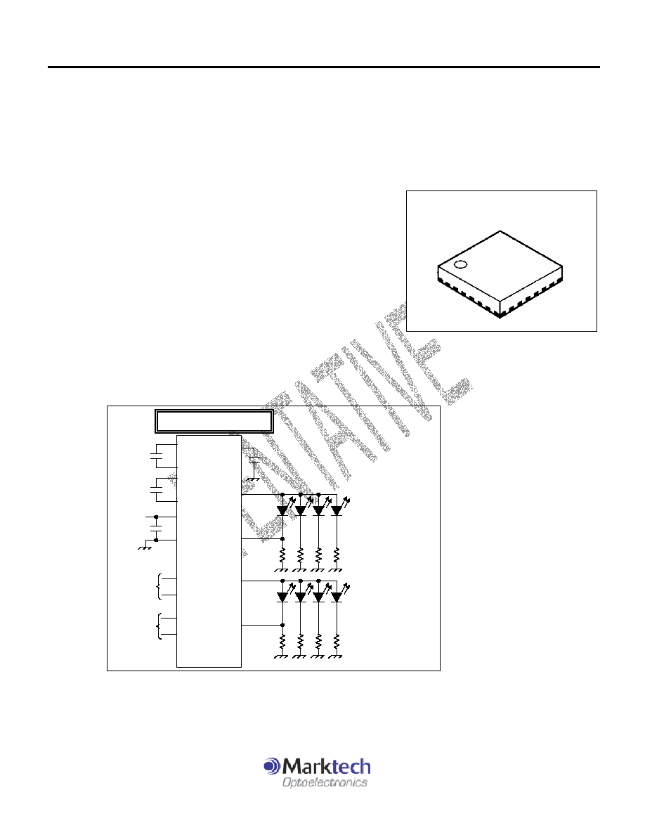
TOSHIBA TB62733FTG
TOSHIBA Bi-CMOS INTEGRATED CIRCUIT SILICON MONOLITHIC
TB62733FTG
Charge Pump type DC/DC Converter for White LED Driver
Application
Charge Pump type DC/DC Converter / White LED Driver
Features
TB62733FTG is charge pump type DC to DC Converter that is accept from
2.8 up to 4.2V input and continue to up converting operation until FB terminal
is equal to 0.4V. (1.5 times up converting)
This device provides over 190mA at Vin=3.9V as the maximum current, and
two outputs structure may help to design the backlighting system such as
the system having two displays that are main and sub LCD displays.
Also, this is used for the power supply of flash lighting by using two outputs
At the same time.
Function
1.5 times Charge Pump type step up DC to DC converter
Features
Utilize Bi-CMOS Process
Package : VQON24(Leadless type)
Input Voltage : 2.8V (Min)
Output Voltage : 4.0V (Min)
Output Current Ability : Greater than 190mA (Usual State)
4 Steps Brightness Control (25%, 50%, 75%, 100%)
Auto Discharge function equipped
Integrated protection circuit TSD (Thermal Shut Down )
Application Diagram
Vin
GND
FB1
SP1
SP1
C3
2.0F
2.85.5V
C4
1.0F
Vout1
C1
C1
C1
1.0F
Brightness
Control
( Steps)
C2
C2
C2
1.0F
QON24-0404-0.65
Weight
0.0g
(Typ.)
CE1
CE2
ON/OFF
Control
FB2
Vout2
Vout0
Company Headquarters
3 Northway Lane North
Latham, New York 12110
Toll Free: 800.984.5337
Fax:
518.785.4725
Web: www.marktechopto.com | Email: info@marktechopto.com
California Sales Office:
950 South Coast Drive, Suite 265
Costa Mesa, California 92626
Toll Free: 800.984.5337
Fax: 714.850.9314
Company Headquarters
3 Northway Lane North
Latham, New York 12110
Toll Free: 800.984.5337
Fax:
518.785.4725
Web: www.marktechopto.com | Email: info@marktechopto.com
California Sales Office:
950 South Coast Drive, Suite 265
Costa Mesa, California 92626
Toll Free: 800.984.5337
Fax: 714.850.9314

TOSHIBA TB62733FTG
This datasheet is tentative, the values and contents are subject to change without any notice.
27-Jul-04 (Rev1.7) TB62733FTG (Page. 2)
Block Diagram
Explanation of Terminals
Terminal
Number
Terminal Name
Function
Comments
1 NC
2
Vout 1
Output 1 Terminal
3
C1+
Capacitance Terminal for Charge Pump Capacitance for Charge Pump
4
C1-
Capacitance Terminal for Charge Pump Capacitance for Charge Pump
5
VIN
Power supply terminal
6 NC
7 NC
8 FB1 Feed Back Control Terminal
Setting feed back voltage by SP terminal (SP1,SP2)
9 NC
10 FB2
Feed Back Control Terminal
Setting feed back voltage by SP terminal (SP1,SP2)
11 NC
12 NC
13 NC
14 GND
Ground
15
C2-
Capacitance Terminal for Charge Pump Capacitance for Charge Pump
16
C2-
Capacitance Terminal for Charge Pump Capacitance for Charge Pump
17 Vout2
Output
2
Terminal
18 NC
19
SP2
Logic Input
Setting of feed back voltage
20
SP1
Logic Input
Setting of feed back voltage
21
Vout0
Output 0
Terminal for output Capacitor
22
NC
23
CE1
Logic Input
On/ Off Control Terminal for Vout 1
24
CE2
Logic Input
On/ Off Control Terminal for Vout 2
Vin
Control
Logic
GND
ON/OFF
C1+
C1
Vout1
C2+
C2
FB1
SP1
SP2
FB2
Feed Back Circuit
FB1Prioritize
FB2In case "Vout"
Not In use
Vout2
CE1
CE2
Vout0
P-GND
TOSHIBA TB62733FTG
This datasheet is tentative, the values and contents are subject to change without any notice.
27-Jul-04 (Rev1.7) TB62733FTG (Page. 3)
Absolute Maximum Ratings
Item Symbol
Conditions
Ratings
Unit
Power Supply
Vin
0.36.0 V
Input Voltage
Vin2
FB/CE/SP Terminal
0.3Vin+0.3 V
Output Current
Iout
250
mA
Power Dissipation
Without PCB
With PCB
357
TBD
Operating Temperature
T
OPR
2585
Storage Temperature
T
STG
55150
Junction Temperature
T
j
150
When the ambient temperature is excess 25 degree C, it should be derating with 1.24mW/degree C.
Recommended Operating ConditionsTopr = -25 � 85 Degree C
Item Symbol
Conditions
Min.
Typ.
Max.
Unit
Power Supply
Vin
2.8
5.5
V
Logic Input Voltage
V
CE
0
Vin V
Input Ripple Voltage
Vin(ripple)
40 mVpp
Capacitance for Charge Pump
C1/2
0.8
1.0
4.0
F
TOSHIBA TB62733FTG
This datasheet is tentative, the values and contents are subject to change without any notice.
27-Jul-04 (Rev1.7) TB62733FTG (Page. 4)
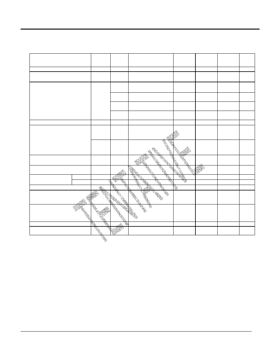
Electrical Characteristics Vin3.6V, T
OPR
25, if it is not specified.
Item Symbol
Measur
ement
Circuit
Measurement Condition
Min.
Typ.
Max.
Unit
Input Voltage
Vin
2.8
5.5
V
Maximum Output Voltage
Vout
Vin=3.0V
Iout=100mA
4.0
V
SP1="L" , SP2="L"
Iout=0mA
(94) 100 (106)
mV
SP1="L" , SP2="H"
Iout=0mA
(188) 200 (212)
mV
SP1="H" , SP2="L"
Iout=0mA
(282) 300 (318)
mV
Feed Back Terminal Voltage
Tolerance of Current Setting
V
FB1
V
FB2
SP1="H" , SP2="H"
Iout=0mA
(376) 400 (424)
mV
Feed Back Terminal Input Current
I
FB
0.5
A
Iout12
Vin=3.2VVout=4.2V
V
FB1
0.4V
90
110
mA
Output Current Ability
Iout
(MAX)
Vin=3.2VVout=4.2V
V
FB1
0.4V
CE1="H"CE2="H"
180
mA
Consumption Current
I
DD
Vin=2.84.2V
Iout=100mA
5 mA
Stand By Consumption Current
I
DDSTB
Iout=0mA
CE1/2="L"
1
A
High V
IH
Logic
Inputs
0.7�Vin
V
Logic Input Voltage
Low V
IL
Logic
Inputs
0.3�Vin V
Logic Input Current
I
leak
Logic
Inputs
0.5
A
Auto Discharging
I
auto
CE1/CE2="L"
Vin=3.6V
Vout=4.0V
7
mA
Vout Rise Time
Vin=2.8VIout=10mA
The transition time
when Vout from 0V to
4V
500
s
Clock Frequency
f
OSC
0.85 1.2 1.55
MHz
Rush Current
I
RUSH
Rush Current at CE
"H"
500
mA
TOSHIBA TB62733FTG
This datasheet is tentative, the values and contents are subject to change without any notice.
27-Jul-04 (Rev1.7) TB62733FTG (Page. 5)
Explanation of Operations
Principle of Basic Operation
The following is the explanation for basic operation of 1.5 time
up converting
1. Charging to C1 and C2
By connecting C1 and C2 through internal Switch as shown in the figure
C1 and C2 is charged. In this case, the C1 is charged up to around
the half of Vin.(Vc1=1/2Vin)
Actually, the voltage is slightly lower than 1/2 Vin due to on resistance
Of internal switch and equivalent resistance of C1.
Thus, C2 is also charged up to 1/2 Vin as well.
2. Out put from C1 and C2 yjat are charged
By connecting C1 and C2 through internal switch as shown in the figure
The charged energy of C1 and C2 output to Vout.
At this time, Vout is added by the voltage charged to C1 and C2, therefore
Vout voltage is approximately 3/2 Vin.
1.5 times Up converting operation
This device performs up converting to output voltage (Vout) that is converted 1.5 times from input voltage. (Vin)
The input voltage will be allowed from 2.8V to 4.2V.
The actual output (Vout) will be differ by the conditions of output current, external parts, application circuit and
so on, because the feed back voltage will be hold at the constant voltage.
The ripple voltage of the output will be approximately 100mV peak to peak.
Vin
Vout
C1
C2
Vin
Vout
C1
C2
3. By repeating the operation 1 and 2 described above, the voltage is
supplied to Vout around 1.5 times of Vin.
TOSHIBA TB62733FTG
This datasheet is tentative, the values and contents are subject to change without any notice.
27-Jul-04 (Rev1.7) TB62733FTG (Page. 6)
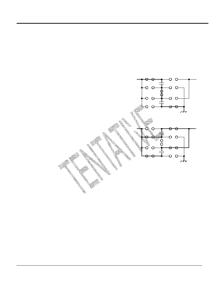
Feed Back Voltage Control
In case of output capacitance C3 is connected to Vout0, capacitance C3 connecting to Vout1 and Vout2
May be omitted.
However, if you have to care about output ripple, it is better C3 connect to each Vout1and Vout2.
This device has a capability of variable control for feed back voltage by using two input such as SP1 and SP2.
Two kind of feed back terminal exist and the following feed back control is performed.
1. Operating both Vout1 and Vout2
: Out1 is controlled by feed back terminal 1. (FB1)
No feed back operation for Out2
2. Operate Vout1 only
: Operation by feed back terminal 1 (FB1)
3. Operate Vout2 only
: Operation by feed back terminal 2 (FB2)
FB1
C3
2.0F
Vout1
R
X
FB2
C3
2.0F
Vout2
R
X
Feed back
Control 1
1. Operate both Vout1 and Vout2
FB1
C3
2.0F
Vout1
R
X
FB2
C3
2.0F
Vout2
R
X
Feed Back
Control 1
Vout 1 operating
LED ON
LED ON
LED ON
Feed back
Control 2
LED OFF

TOSHIBA TB62733FTG
This datasheet is tentative, the values and contents are subject to change without any notice.
27-Jul-04 (Rev1.7) TB62733FTG (Page. 7)
Truth Table for Current Control
SP1 SP2 FB
Control
Voltage LED Current at Resistor(R
X
)20
L L
0.1V
5mA
L H
0.2V
10mA
H L
0.3V
15mA
H H
0.4V
20mA
The feed back voltage is set by input signal (SP1 and SP2)
As shown in the following table, the current value of LED is obtained by the following equation.
I
LED
V
FB
R
X
The brightness control is available with feed back voltage control.
FB1
C3
2.0F
Vout1
R
X
FB2
C3
2.0F
Vout2
R
X
Feed Back
Control 2
3. Vout 2 Operating
LED ON
Truth Table (CE1 and CE2)
CE1
CE2
Output Terminal
Feed Back Control
L L
None
None
H L
Vout1
FB1
L H
Vout2
FB2
H H
Vout1,Vout2
FB1FB2
LED OFF
Soft Start Function
This device is integrated Soft start function. When the power supply is ON or output is started to operate, the transition
time is controlled in order to decrease the rush current.
Thermal Shut Down Function
This device has Thermal Shutdown Function to protect from thermal damage when the output is shorted.
The temperature to operate this function is set around from 120 to 160 degree C. (This is not guaranteed Value.)
The selection of Capacitor for Charge Pump, input and output
The input capacitor is effective to decrease the impedance of power supply and also input current is averaged.
The input capacitor should be selected by impedance of power supply, it is better to choose with lower ESR
(Equivalent Series Resistor). (i.e. ceramic capacitor etc.) Regarding to the capacitance values, it is recommended to
choose in the range from 0.8 uF to 10 uF, however larger than 1 uF should be better.
The output capacitor is effective to decrease the ripple noise of the output line. Also, it is better to choose the capacitor.)
Regarding to the capacitance values, it is recommended to
choose in the range from 0.8 uF to 10 uF, however larger than 2 uF should be better.
The capacitor for charge pump operation is also selected the capacitor with low ESR. .) Regarding to the
capacitance values, it is recommended to choose in the range from 0.8 uF to 10 uF, however larger than 1 uF should be
better.

TOSHIBA TB62733FTG
This datasheet is tentative, the values and contents are subject to change without any notice.
27-Jul-04 (Rev1.7) TB62733FTG (Page. 8)
Application Example
This device has a large drive capability (Iout Max : Larger than 190mA), if in case of driving LED at 20mA each, this device
can drive up to 9 LEDs max.
1. In use of LCD backlighting (Main and Sub Displays)
In case of driving the back light system both for main display and sub display, this device can be used for this application
With securing the output current of maximum 190mA.
Also, Vout 1 has a drive capability up to 110mA, so it is allowed to change the system thet Vout 1 can drive 6 LEDs
(backlight for main display), then Vout 2 drives 2LEDs for the backlight of sub display as showing in Application Figure 2.
The LED brightness balance is adjusted by using FB1 and FB2.
Vin
GND
FB1
SP1
SP2
2.84.2V
C4
1.0F
Vout1
C1
C1
C1
1.0F
C2
C2
C2
1.0F
20 20 20 20
Sub Display
1LED
Total 80 mA
0.4V
CE1
CE2
20 20 20 20
0.4V
FB2
Vout2
Main Display
1LED : 20
Total 80 mA
Vin
GND
FB1
SP1
SP2
2.84.2V
C4
1.0F
Vout1
C1
C1
C1
1.0F
C2
C2
C2
1.0F
20 20 20 20
Sub Display
1 LED 20 mA
Total 40 mA
0.4V
CE1
CE2
20 20
0.4V
FB2
Vout2
Main Display
1 LED18
Total 108 mA
20 20
Application Figure 1
Application Figure 2
C3
2.0F
Vout0
C3
2.0F
Vout0
These figures are showing as the standard application example. The current values or so are considered whenever it is designed.

TOSHIBA TB62733FTG
This datasheet is tentative, the values and contents are subject to change without any notice.
27-Jul-04 (Rev1.7) TB62733FTG (Page. 9)
2. In case of driving both Backlighting (Main/Sub Displays) and Key pad Illumination
By using external MOS FET, the system of driving for main , sub display and Key pad Illumination is also composed.
3. LCD Backlight system (Only Main Display)
In case sub display is not connected, Vout 2 is terminated when CE2 terminal fix to the ground, then only Vout 1 can be
operated. In case of this application, Vout2 and FB2 should be open connection.
In case of using this device with 190mA of total output current, as shown application figure 5, Vout 1 and Vout 2 are connected
as common output. In this case, CE1 and CE2 are applied with common signal, and FB2 should be open connection.
Key Pad
1 LED5 mA
Total 10 mA
2.84.2V
20 50
Vin
GND
FB1
SP1
SP2
C4
1.0F
Vout1
C1
C1
C1
1.0F
C2
C2
C2
1.0F
20 20 20 20
Sub Display
1 LED : 20 mA
Total 60 mA
0.4V
CE1
CE2
20 20 20
0.4V
FB2
Vout2
Main Display
1 LED20 mA
Total 80 mA
Application Figure 3
2.84.2V
Vin
GND
FB1
SP1
SP2
C4
1.0F
Vout1
C1
C1
C1
1.0F
C2
C2
C2
1.0F
20 20 20 20
0.4V
CE1
CE2
FB2
Vout2
Main Display
20
TOTAL 80
NC
NC
Application Figure 4
C3
2.0F
Vout0
C3
2.0F
Vout0
These figures are showing as the standard application example. The current values or so are considered whenever
it is
designed.
These figures are showing as the standard application example. The current values or so are considered whenever it is designed.
TOSHIBA TB62733FTG
This datasheet is tentative, the values and contents are subject to change without any notice.
27-Jul-04 (Rev1.7) TB62733FTG (Page. 10)
In case of output capacitance C3 is connected to Vout0, capacitance C3 connecting to Vout1 and Vout2 may be omitted.
The current value is just example for the explanation of this device function, please note that power dissipation should be taken
care when the system is designed or define the current value.
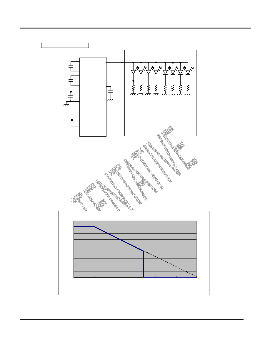
Power Dissipation
If the ambient temperature is exceed than 25 degree C , it is derated with derating factor of 1.24mW/Degree C.
In case of assembled SEMI PCB((75 mm x 114 mm) ; 155 degree C/W
2.84.2V
Vin
GND
FB1
SP1
SP2
C3
2.0F
90mA
C4
1.0F
Vout1
C1
C1
C1
1.0F
C2
C2
C2
1.0F
20 20 20
0.4V
CE1
CE2
FB2
Vout2
Main Display
1 LED
TOTAL
20
Application Figure 5
C3
2.0F
90mA
20 20 20
20
Vout0
C
2.0F
The characteristics of P ow er D issipationA ssbled on P C B
0
0.1
0.2
0.3
0.4
0.5
0.6
0.7
0.8
0.9
0
25
50
75
100
125
150
A m bient Tem perature[
Po
we
r
D
iss
i
p
a
t
i
o
n
These figures are showing as the standard application example. The current values or so are considered whenever
it is
designed.

TOSHIBA TB62733FTG
This datasheet is tentative, the values and contents are subject to change without any notice.
27-Jul-04 (Rev1.7) TB62733FTG (Page. 11)
Output Voltage
Vo=Vf(LED)+0.4V
2.0
2.2
2.4
2.6
2.8
3.0
3.2
3.4
3.6
3.8
4.0
2.5
3.0
3.5
4.0
4.5
Input V oltage [V ]
Output Voltage [V
]
Io=200m A
Io=100m A
Io=40m A
Ef f iciency
0%
10%
20%
30%
40%
50%
60%
70%
80%
90%
100%
2.5
3.0
3.5
4.0
4.5
Input V oltage [V ]
Effi
ci
e
n
cy(%)
Io= 40m A
Io=100m A
Io=200m A
O utput V oltage operate ability
1.0
1.5
2.0
2.5
3.0
3.5
4.0
0
50
100
150
200
250
300
O utput C urrent [m A }
Output Voltage [V
]
V in=2.7V
V in=3.0V
V in=3.3V
Feedback V oltage
V=0.4V
220.0
240.0
260.0
280.0
300.0
320.0
340.0
360.0
380.0
400.0
420.0
2.5
3.0
3.5
4.0
4.5
Input V oltage [V ]
Feedback Voltage [mV]
Io=200m A
Io=100m A
Io=40m A
TOSHIBA TB62733FTG
This datasheet is tentative, the values and contents are subject to change without any notice.
27-Jul-04 (Rev1.7) TB62733FTG (Page. 12)
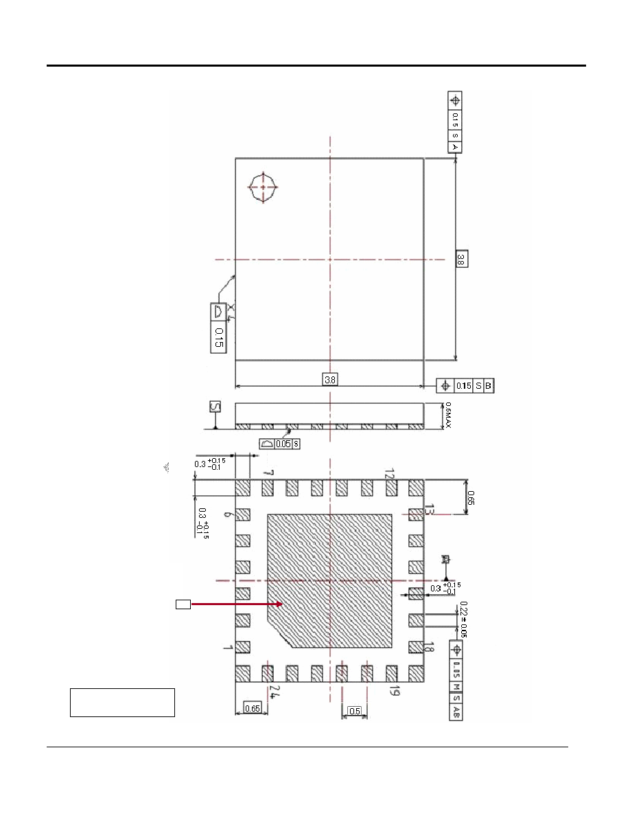
Package Dimension
Weight : g (typ.)
2.3