 | –≠–ª–µ–∫—Ç—Ä–æ–Ω–Ω—ã–π –∫–æ–º–ø–æ–Ω–µ–Ω—Ç: TB6581H | –°–∫–∞—á–∞—Ç—å:  PDF PDF  ZIP ZIP |

TB6581H/HG
2004-03-01
1
TOSHIBA Bi-CMOS Power Integrated Circuit Multi-Chip Package (MCP)
TB6581H/HG
3-Phase Full-Wave Sine-Wave PWM Brushless Motor Controller
The TB6581H/HG is a high-voltage PWM BLDC motor driver.
The product integrates the TB6551F/FG sine-wave controller and
the TPD4103AK high-voltage driver in a single package ("2-in-1").
It is designed to change the speed of a BLDC directly motor by
using a speed control signal (analog) from a microcontroller.
Features
∑
A sine wave PWM drive controller and a high-voltage driver
integrated in a single package.
∑
IGBTs arranged in three half-bridge units
∑
Triangle wave generator (carrier frequency = f
osc
/254 (Hz))
∑
Dead-time insertion (1.9 µs)
∑
High-side bootstrap supply
∑
Bootstrap diode
∑
Overcurrent protection, thermal shutdown, and undervoltage lockout
∑
On-chip regulator (V
reg
= 7 V (typ.), 30 mA (max),
Vrefout = 5 V (typ.), 30 mA (max))
∑
Operating power supply voltage range: V
CC
= 13.5~16.5 V
∑
Motor power supply operating voltage range: VB = 50~400 V
Weight:
HZIP25-P-1.00K: 7.7 g (typ.)
TB6581HG:
TB6581HG is a Pb-free product.
The following conditions apply to solderability:
*Solderability
1.
Use of Sn-63Pb solder bath
*solder bath temperature = 230∞C
*dipping time = 5 seconds
*number of times = once
*use of R-type flux
2.
Use of Sn-3.0Ag-0.5Cu solder bath
*solder bath temperature = 245∞C
*dipping time = 5 seconds
*the number of times = once
*use of R-type flux

TB6581H/HG
2004-03-01
2
Pin Description
Pin No.
Symbol
Description
Function
1
PGND
Grounding pin
Power ground
2
VREG
Reference voltage output Connected to pin 5. 7 V (typ.), 30 mA (max)
3
IS
IGBT emitter pin
For connecting a current sensing resistor to ground.
4
NC
Not connected
This pin is left open and can be used as a jumper on a PCB.
5 V
CC7
Signal control power
supply pin
Connected to pin 2. The control stage operating voltage: V
CC
=
6 to 10 V
6 V
refout
Reference
voltage
output 5 V (typ.), 30 mA (max)
For connecting a bypass capacitor for internal V
DD
.
7
Idc
Current limit input
DC link input
Reference potential of 0.5 V. This pin has a filter (
-
1
µ
s).
8
SGND
Grounding pin
Signal ground
9 X
in
Clock
input
10 X
out
Clock
output
These pins have a feedback resistor. For connecting to a crystal oscillator.
11
Ve
Voltage command input
This pin has a pull-down resistor.
12 HU
U-phase position sensing
input
13 HV
V-phase position sensing
input
14 HW
W-phase position
sensing input
If the position sensing inputs are all HIGH or LOW, the outputs are turned off.
This pin has a pull-up resistor.
15
LA
Lead angle control input
0 to 58∞ in 32 steps
16
FG
FG signal output
This pin drives three pulses per rotation.
17
REV
Reverse rotation signal
For reverse rotation detection.
18 BSU
Bootstrap supply
(phase U)
For connecting a bootstrap capacitor to the U-phase output.
19 U
U-phase
output
pin
20 BSV
Bootstrap supply
(phase V)
For connecting a bootstrap capacitor to the V-phase output.
21 V
V-phase
output
pin
22 BSW
Bootstrap supply
(phase W)
For connecting a bootstrap capacitor to the W-phase output.
23
W
W-phase output pin
24 VB
High-voltage power
supply pin
Power supply pin for driving a motor.
25 V
CC15
Power supply pin for the
power stage
Power stage operating range: V
CC
=
15 V

TB6581H/HG
2004-03-01
3
Pin Assignment
Maximum Ratings
(Ta
=
25∞C)
Characteristics Symbol
Rating
Unit
V
CC7
12
V
CC15
18
Power supply voltage
VB 500
V
V
in (1)
-
0.3 to V
CC1
(Note 1)
Input voltage
V
in (2)
-
0.3 to 5.5
(Note 2)
V
PWM output current
I
OUT
2
(Note 3)
A
Power dissipation
P
D
40
(Note 4)
W
Operating temperature
T
opr
-
30 to 115
(Note 5)
∞C
Storage temperature
T
stg
-
50 to 150
∞C
Note 1: V
in (1)
pin: V
e
, LA
Note 2: V
in (2)
pin: I
dc
, HU, HV, HW
Note 3: Apply pulse
Note 4: Package thermal resistance (
j-c
=
1∞C/W) with an infinite heat sink at Ta
=
25∞C
Note 5: The operating temperature range is determined according to the P
D
MAX
-
Ta characteristics.
V
CC7
1
PGND
VREG
IS
Vrefout Xout
Xin
BSU
U
BSV
V
BSW
W
VB
V
CC15
SGND FG
HU
NC
HV
HW
Ve
LA
REV
2 3 4 5 6
7 8 9 10 11 12 13 14 15 16 17 18 19 20 21 22 23 24 25
Idc

TB6581H/HG
2004-03-01
4
Recommended operating conditions
(Ta
=
25∞C)
Characteristics Symbol
Min
Typ.
Max
Unit
V
CC7
6 7
10
Power supply voltage
V
CC15
13.5
15 16.5
V
Crystal oscillator frequency
X
in
2 4 5
MHz
Motor power supply voltage
VB
50
280
400
V
Output current
Iout
1 2 A
P
D
Max ≠ Ta
Ambient temperature Ta (∞C)
Pow
e
r
dis
s
ip
at
io
n
P
D
ma
x
(
W
)
(1)
(2)
(3)
25
0
150
0
80
75
40
100
20
60
50
125
(1) INFINITE HEAT SINK
R
j-c
=
1∞C/W
(2) HEAT SINK (R
HS
=
3.5∞C/W)
R
j-c
+
R
HS
=
4.5∞C/W
(3) NO HEAT SINK
R
j-a
=
39∞C/W

TB6581H/HG
2004-03-01
5
Electrical Characteristics
(Ta
=
25∞C)
Characteristics Symbol Test
Condition Min
Typ.
Max
Unit
I
B
V
B
=
400 V
0.1 0.5
I
CC15
V
reg
=
OPEN, V
CC
=
15 V
1.1 3
I
CC7
V
refout
=
OPEN, V
CC
=
7 V
3 6
mA
I
BS (ON)
V
BS
=
15 V, high-side ON
260 410
Current dissipation
I
BS (OFF)
V
BS
=
15 V, high-side OFF
230 370
µ
A
I
in
(LA)
Vin
=
5 V, LA
25 50
I
in
(V
e
) Vin
=
5 V, V
e
35 70
Input current
I
in
(Hall)
Vin
=
0 V, HU, HV, HW
-
50
-
25
µ
A
HIGH
V
refout
-
1
V
refout
V
in
(Hall)
LOW
HU, HV, HW
0.8
HIGH PWM
Duty
100%
5.1 5.4 5.7
Middle Refresh
Start motor operation
1.8
2.1
2.4
Input voltage
V
in
(V
e
)
LOW Turned-off
Refresh
0.7 1.0 1.3
V
Input hysteresis voltage
V
H
HU, HV, HW
(Note 6)
0.3
V
V
DT
HU, HV, HW
X
in
=
4.19 MHz
4.0
Input delay time
V
DC
Idc
X
in
=
4.19 MHz
4.0
µ
s
V
CEsat
H V
CC
=
15 V, IC
=
0.5 A
2.4 3
Output saturation voltage
V
CEsat
L V
CC
=
15 V, IC
=
0.5 A
2.4 3
V
V
FG (H)
I
OUT
=
1 mA
FG
V
refout
-
1.0
V
refout
-
0.2
V
FG (L)
I
OUT
=
-
1 mA
FG
0.2 1.0
V
refout
I
OUT
=
30 mA
V
refout
4.5 5.0 5.5
Output voltage
V
reg
I
OUT
=
30 mA
6.5
7
7.5
V
V
F
H IF
=
0.5 A, high-side
1.3 2.0
FRD forward voltage
V
F
L IF
=
0.5 A, low-side
1.3 2.0
V
BSD forward voltage
V
F (BSD)
IF
=
500
µ
A
0.9 1.2 V
Current detection
V
dc
I
dc
0.47
0.5
0.53
V
TSD
150 165 200
Thermal shutdown protection
TSDhys
(Note 7)
20
∞C
V
CC15
(H)
Undervoltage positive-going threshold
10.5
11.5
12.5
V
CC15
undervoltage protection for
driver
V
CC15
(L)
Undervoltage negative-going threshold
10
11
12
V
VBS (H)
Undervoltage positive-going threshold
8.5
9.5
10.5
VBS undervoltage protection for driver
VBS (L)
Undervoltage negative-going threshold
8
9
10
V
V
CC7
(H)
Undervoltage positive-going threshold
4.2
4.5
4.8
V
CC7
undervoltage protection for
controller
V
CC7
(L)
Undervoltage negative-going threshold
3.7
4.0
4.3
V
t
on
V
BB
=
280 V, V
CC
=
15 V, IC
=
0.5 A
1.5 3
Output turn-on/-off delay time
t
off
V
BB
=
280 V, V
CC
=
15 V, IC
=
0.5 A
1.2 3
µ
s
Dead time
tdead
X
in
=
4.19 MHz
1.5
1.8
µ
s
FRD reverse recovery time
t
rr
V
BB
=
280 V, V
CC
=
15 V, IC
=
0.5 A
200
ns
Note 6 and Note 7: Toshiba does not implement testing before shipping.

TB6581H/HG
2004-03-01
6
Functional Description
1. Basic
operation
The motor is driven by the square-wave turn-on signal based on a positional signal. When the positional
signal reaches number of rotations f
= 5 Hz or higher, the rotor position is estimated according to the
positional signal and a modulation wave is generated. The modulation wave and the triangular wave are
compared; then the sine-wave PWM signal is generated and the motor is driven.
From start to 5 Hz: When driven by square wave (120∞ turn-on) f
= f
osc
/(2
12
◊ 32 ◊ 6)
5 Hz~: When driven by sine-wave PWM (180∞ turn-on); when f
osc
= 4 MHz, approx. 5 Hz
2. V
e
voltage command input and bootstrap power supply
(1)
Voltage command input: When V
e
<
= 1.0 V
U, V and W signals are stopped to protect IGBTs
(2)
Voltage command input: When 1.0 V
< V
e
<
= 2.1 V
The low-side IGBTs are turned on at a fixed frequency (carrier frequency) (duty cycle: 8%).
(3)
Voltage command input: When V
e
> 2.1 V
The U, V and W signals are driven out during sine wave drive.
The low-side IGBTs are forced to on at fixed frequency (carrier frequency) during square-wave drive
(duty cycle: 8%).
Note 1: At startup, the low-side IGBTs must be turned on for a fixed period at 1.0 V
<
V
e
<
=
2.1 V to charge the
high-side IGBT power supply.
3. Dead time function: upper/lower transistor output off-time
When the motor is driven by sine-wave PWM, dead time is digitally generated inside the IC to prevent
short circuit caused by the simultaneously turning on of upper and lower external power devices. When a
square wave is generated in full-duty cycle mode, the dead time function is turned on to prevent a short
circuit.
Internal Counter
T
OFF
8/f
osc
1.9
µ
s
T
OFF
values above are obtained when fosc = 4.19 MHz.
f
osc
= reference clock (crystal oscillation)
4. Correcting the lead angle
The lead angle can be corrected in the turn-on signal range from 0 to 58∞ in relation to the induced
voltage.
Analog input from LA pin (0 V to 5 V divided by 32)
0 V
= 0∞
5 V
= 58∞ (when more than 5 V is input, 58∞)
(1)
(2) (3)
100%
2.1 V
1.0 V
5.4 V
Ve
PWM duty cycle
(1) 0 to 1.0 V: Reset state (All outputs are off.)
(2) Ve
=
1.0 to 2.1 V: Startup operation
(duty cycle of 8% for the low-side IGBTs)
(3) Ve
=
2.1 to 5.4 V: Running state
(5.4 V or higher: PWM duty cycle = 100%)

TB6581H/HG
2004-03-01
7
5. Setting the carrier frequency
This function sets the triangular wave cycle (carrier cycle) necessary for generating the PWM signal.
(The triangular wave is used for forcibly turning on the lower transistor when the motor is driven by
square wave.)
Carrier cycle
= f
osc
/252 (Hz) f
osc
= reference clock (crystal oscillation)
6. Outputting the reverse rotation detection signal
This function detects the motor rotation direction every electrical angle of 360∞. This function judges
whether the actual direction of a rotating motor coincides with that of the internal reference voltage.
Actual Motor Rotating Direction
REV Pin
Drive Mode
CW (forward)
HIGH
Square waveform (120∞ turn-on mode)
CCW (reverse)
LOW
Sine-wave waveform (180∞ turn-on mode)
*:
CW or CCW of the motor is determined by the direction of the Hall signal, which is specified in the timing
chart on page 9.
*:
When the REV pin is set to LOW, and the Hall signal is higher than 5 Hz, sine-wave drive mode is turned
on.
7. Protecting
input
pin
(1)
Overcurrent protection (Pin I
dc
)
When the DC-link-current exceeds the internal reference voltage, gate block protection is performed.
Overcurrent protection is released for each carrier frequency.
Reference voltage
= 0.5 V (typ.)
(2)
Positional signal abnormality protection
Output is turned off when the positional signal is HHH or LLL; otherwise, it is restarted.
(3)
Monitor protection for V
CC7
/ V
CC15
low supply voltage
For power supply on/off outside the operating voltage range, the U, V and W drive outputs are
turned off and the motor is stopped when there is a power supply fault.
< V
CC7
>
< V
CC15
>
Turn-off drive output
Turn-off drive output
Turn-on drive output
Power supply voltage 4.5 V (typ.)
4.0 V (typ.)
GND
V
B
V
CC7
Output
Turn-off drive output
Turn-on drive output
Power supply voltage 11.5 V (typ.)
11.0 V (typ.)
GND
V
B
V
CC15
Turn-off drive output
Output

TB6581H/HG
2004-03-01
8
(4)
Monitor protection for V
BS
Bootstrap power supply
When V
BS
power supply is lowered, the high-side IGBT is turned off.
(5)
Overheat protection
The overheat protection circuit will operate and all IGBTs will be turned off if the chip temperature
becomes abnormally high due to internal or external heat generation.
T
SD
= 165∞C (typ.)
T
SDhys
= 20∞C (typ.)
After the overheat protection circuit is turned on, the return temperature is 145∞C (typ.).
Turn-off high-side IGBT
Turn-off high-side IGBT
High-side IGBT
V
BS
(Output -BS)
9.5 V (typ.)
9.0 V (typ.)
Output

TB6581H/HG
2004-03-01
9
Timing Chart
∑
CW (forward) mode (CW mode means that the Hall signal is input in the order shown below.)
∑
CCW (reverse) mode (CCW mode means that the Hall signal is input in the order shown below.)
Motor drive
output
waveform
(line voltage)
Hall signal
(input)
H
u
H
v
H
w
FG signal
(output)
FG
Turn-on signal
when driven
by square wave
(inside the IC)
U
V
W
X
Y
Z
REV signal
(output)
REV
(HIGH
)
V
uv
V
vw
V
wu
* The waveform of actual
operation is the PWM
Motor drive
output
waveform
(line voltage)
H
u
H
v
H
w
FG signal
(output)
FG
REV
(LO
W)
Modulation
waveform when
driven by sine
wave
(inside of IC)
S
u
S
v
S
w
Hall signal
(input)
REV signal
(output)
V
uv
V
vw
V
wu
* The waveform of actual
operation is the PWM
TB6581H/HG
2004-03-01
10
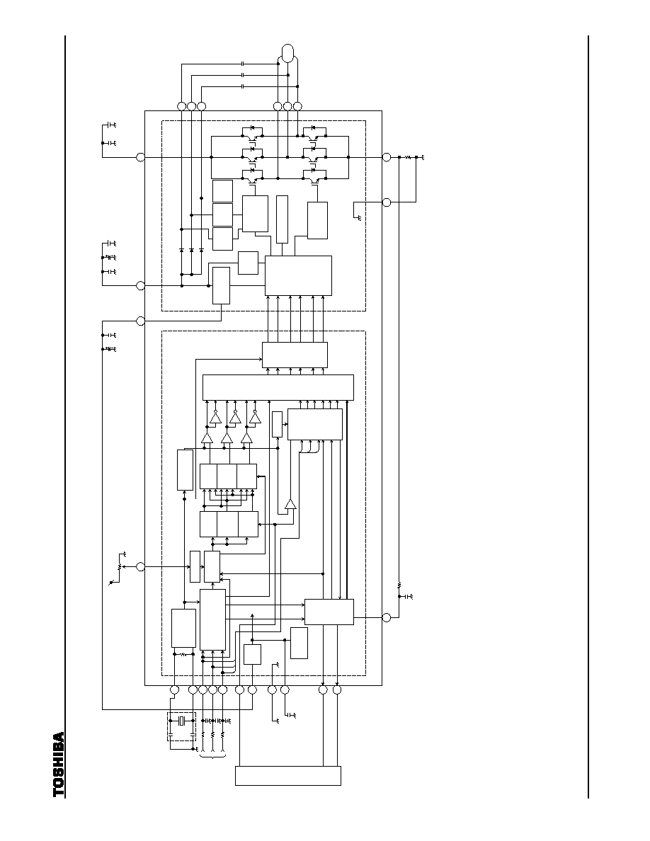
Example of Application Circuit
System clock
generator
Position detector
Counter
5-bit AD
Triangular wave
generator 6-bit
Output
waveform
generator
Selecting
data
Switching
120∞/180∞
&
gate
block
protection
on/off
Setting
dead time
Charger
120∞-
turn-on
matrix
Power-on
reset
Protection
&
reset
15
9
10
12
13
14
11
5
8
6
16
17
Phase
matchin
4 bit
FG
Rotating
direction
ST/SP
ERR
GB
Comparator
Comparator
PWM
HU
HV
HW
120∞/180∞
Phase
U
X
in
X
out
HU
HV
HW
V
e
V
CC7
S-GND
V
refout
FG
REV
LA
U
X
V
Y
W
Z
BRK (CHG)
V
refout
MCU
Regula
tor
Internal
reference
voltage
Low-side
driver
V
REG
Input control
BSV
BSU
V
B
BSW
U
V
W
High-side
level shift
driver
2
HU
HV
HW
LU
LV
LW
18
20
22
19
21
23
Under-
voltage
protection
7-V
Regulator
C
10
C
11
C
12
C
3
C
2
C
1
R
1
R
2
R
3
Hall IC
input
X
1
C
4
7 Idc
1
24
3
V
CC15
25
P-GND
IS
R
5
C
5
R
4
C
9
C
8
15 V
Power supply
for motor
C
7
C
6
Motor
(Controller) (Driver)
Phase
V
Phase
W
Comparator
Comparator
Under-
voltage
protection
Under-
voltage
protection
Under-
voltage
protection
Thermal shutdown

TB6581H/HG
03/12/25
11
External Parts
Symbol Purpose
Recommended
value
Note
X
1
Internal clock generation
4.19 MHz
(Note 1)
C
1
, C
2
, C
3
10
V/1000
pF
R
1
, R
2
, R
3
Noise absorber
10 k
(Note 2)
C
4
V
refout
oscillation protection
10 V/0.1
µ
F~1.0
µ
F (Note
3)
C
5
10
V/1000pF
R
4
Noise absorber
5.1 k
(Note 2)
R
5
Overcurrent
detection
0.62
±
1% (1 W)
(Note 4)
C
6
16
V/1.0
µ
F~10
µ
F
C
7
V
REG
power supply stability
10 V/1000 pF
(Note 3)
C
8
25
V/0.1
µ
F
C
9
V
CC15
power supply stability
25 V/10
µ
F
(Note 3)
C
10
, C
11
, C
12
Bootstrap
capacitor
25
V/2.2
µ
F (Note
5)
Note 1: For carrier frequency and dead time, connect a 4.19 MHz ceramic resonator.
Note 2: These parts are used as a low-pass filter for noise absorption. Test to confirm noise filtering, then set the
filter time-constant.
Note 3: This part is used as a capacitor for power supply stability. Adjust the part to the application environment as
required. When mounting, place it as close as possible to the base of the leads of this product to improve
the noise elimination.
Note 4: This part is used to set the value for overcurrent detection. I
out (max)
=
V
dc
˜
R
5
(V
dc
=
0.5 V (typ.))
Note 5: The required bootstrap capacitance value varies according to the motor drive conditions. The voltage stress
for the capacitor is the value of V
CC15
.
Other Precautions
A short circuit between the outputs, or between output and supply or ground may damage the device. Peripheral
parts may also be damaged by overvoltage and overcurrent. Design the output lines, V
CC
and GND lines so that
short circuits do not occur.
Also be careful not to insert the IC in the wrong direction because this could destroy the IC.
In turning on the power, first supply Vcc15 and confirm its stability; then apply Vcc7 and the driving input signal.
Vcc15 and VB may be turned on in either order. In turning off the power, take care not to cut off the VB line by
relay while the motor is spinning. Doing so may cause the IC to break down by cutting the current-producing route
for VB.
The TB6581H/HG is sensitive to electrostatic discharge. Handle with care.
The product should be mounted by the solder-flow method. The preheating time is from 60 to 120 seconds at
150∞C. The maximum heat is 260∞C, to be applied within 10 seconds and as far as the lead stopper.

TB6581H/HG
03/12/25
12
Package Dimensions
Weight: 7.7 g (typ.)

TB6581H/HG
03/12/25
13
Notes on contents
1. Block Diagrams
Some functional blocks, circuits, or constants may be omitted or simplified in the block diagram for explanatory
purposes.
2. Equivalent Circuits
The equivalent circuit diagrams may be simplified or some parts of them may be omitted for explanatory
purposes.
3. Timing Charts
Timing charts may be simplified for explanatory purposes.
4. Maximum Ratings
The absolute maximum ratings of a semiconductor device are a set of specified parameter values that must not
be exceeded during operation, even for an instant.
If any of these ratings are exceeded during operation, the electrical characteristics of the device may be
irreparably altered, in which case the reliability and lifetime of the device can no longer be guaranteed.
Moreover, any exceeding of the ratings during operation may cause breakdown, damage and/or degradation in
other equipment. Applications using the device should be designed so that no maximum rating will ever be
exceeded under any operating conditions.
Before using, creating and/or producing designs, refer to and comply with the precautions and conditions set
forth in this document.
5. Application Circuits
The application circuits shown in this document are provided for reference purposes only. Thorough evaluation
is required in the mass production design phase.
In furnishing these examples of application circuits, Toshiba does not grant the use of any industrial property
rights.
6. Test Circuits
Components in test circuits are used only to obtain and confirm device characteristics. These components and
circuits are not guaranteed to prevent malfunction or failure in application equipment.
Handling of the IC
Ensure that the product is installed correctly to prevent breakdown, damage and/or degradation in the product
or equipment.
Over-current protection and heat protection circuits
These protection functions are intended only as a temporary means of preventing output short circuits or other
abnormal conditions and are not guaranteed to prevent damage to the IC.
If the guaranteed operating ranges of this product are exceeded, these protection features may not operate
and some output short circuits may result in the IC being damaged.
The over-current protection feature is intended to protect the IC from temporary short circuits only.
Short circuits persisting over long periods may cause excessive stress and damage the IC. Systems should
be configured so that any over-current condition will be eliminated as soon as possible.
Counter-electromotive force
When the motor reverses or stops, the effect of counter-electromotive force may cause the current to flow to the
power source.
If the power supply is not equipped with sink capability, the power and output pins may exceed the maximum
rating.
The counter-electromotive force of the motor will vary depending on the conditions of use and the features of
the motor. Therefore make sure there will be no damage to or operational problem in the IC, and no damage to
or operational errors in peripheral circuits caused by counter-electromotive force.

TB6581H/HG
03/12/25
14
∑
The information contained herein is subject to change without notice.
∑
The information contained herein is presented only as a guide for the applications of our products. No
responsibility is assumed by TOSHIBA for any infringements of patents or other rights of the third parties which
may result from its use. No license is granted by implication or otherwise under any patent or patent rights of
TOSHIBA or others.
∑
TOSHIBA is continually working to improve the quality and reliability of its products. Nevertheless, semiconductor
devices in general can malfunction or fail due to their inherent electrical sensitivity and vulnerability to physical
stress. It is the responsibility of the buyer, when utilizing TOSHIBA products, to comply with the standards of
safety in making a safe design for the entire system, and to avoid situations in which a malfunction or failure of
such TOSHIBA products could cause loss of human life, bodily injury or damage to property.
In developing your designs, please ensure that TOSHIBA products are used within specified operating ranges as
set forth in the most recent TOSHIBA products specifications. Also, please keep in mind the precautions and
conditions set forth in the "Handling Guide for Semiconductor Devices," or "TOSHIBA Semiconductor Reliability
Handbook" etc..
∑
The TOSHIBA products listed in this document are intended for usage in general electronics applications
(computer, personal equipment, office equipment, measuring equipment, industrial robotics, domestic appliances,
etc.). These TOSHIBA products are neither intended nor warranted for usage in equipment that requires
extraordinarily high quality and/or reliability or a malfunction or failure of which may cause loss of human life or
bodily injury ("Unintended Usage"). Unintended Usage include atomic energy control instruments, airplane or
spaceship instruments, transportation instruments, traffic signal instruments, combustion control instruments,
medical instruments, all types of safety devices, etc.. Unintended Usage of TOSHIBA products listed in this
document shall be made at the customer's own risk.
∑
The products described in this document are subject to the foreign exchange and foreign trade laws.
∑
TOSHIBA products should not be embedded to the downstream products which are prohibited to be produced
and sold, under any law and regulations.
030619EBA
RESTRICTIONS ON PRODUCT USE