 | ÐлекÑÑоннÑй компоненÑ: TC35273 | СкаÑаÑÑ:  PDF PDF  ZIP ZIP |
Äîêóìåíòàöèÿ è îïèñàíèÿ www.docs.chipfind.ru
MPEG-4 Audiovisual Codec LSI
Preliminary
TC35273
TOSHIBA Confidential
2000-4-27
1/23
Version
0.90
TOSHIBA MPEG-4 Audiovisual LSI
TC35273
Tentative Technical Data Sheet
MPEG-4 Audiovisual LSI
Features
U
TC35273 is an MPEG-4 audiovisual codec LSI
which supports 3GPP 3G-324M video telephony
system. MPEG-4 video codec with QCIF (176x144
pixel) at 15 frames/s, AMR (Adaptive Multi Rate)
speech codec, and ITU-T H.223 are executed
concurrently at around 70MHz clock rate.
U
Three signal processing units, an MPEG-4 video
codec, a speech codec / audio decoder, and a
multiplex / demultiplex unit, are integrated on a
single chip.
U
A 12-Mbit embedded DRAM is integrated as a shared memory for the three signal processing
units. The embedded DRAM helps to reduce power consumption without performance
degradation.
U
Each signal processing unit consists of a 16-bit RISC processor and dedicated hardware
accelerators so as to bring programmability, high performance and low power consumption.
U
Firmware programs for the RISCs are downloaded into the embedded DRAM before starting
operation. Various applications are performed by choosing an appropriate firmware.
U
General host interface are adopted in order to support various host CPU.
U
2.5x to 6x of PLL is integrated on the chip for easy system integration.
·
TOSHIBA continually is working to improve the quality and the reliability of its products. Nevertheless, semiconductor
devices in general can malfunction or fail due to their inherent electrical sensitivity and vulnerability to physical stress. It is the
responsibility of the buyer, when utilizing TOSHIBA products, to observe standards of safety, and to avoid situations in which a
malfunction or failure of a TOSHIBA product could cause loss of human life, bodily injury or damage to property. In developing
your designs, please ensure that TOSHIBA products are used within specified operating ranges as set forth in the most recent
products specifications. Also, please keep in mind the precautions and conditions set forth in the TOSHIBA Semiconductor
Reliability Handbook.
·
The products described in this document are subject to foreign exchange and foreign trade laws.
·
The information contained herein is presented only as a guide for the applications of our products. No responsibility is
assumed by TOSHIBA CORPORATION for any infringements of intellectual property or other rights of the third parties which
may result from its use. No license is granted by implication or otherwise under any intellectual property or other rights of
TOSHIBA CORPORATION or others.
·
The information contained herein is subject to change without notice.
P-FBGA201-1515-0.80A5

MPEG-4 Audiovisual Codec LSI
Preliminary
TC35273
TOSHIBA Confidential
2000-4-27
2/23
Version
0.90
·
The circuit contained herein is presented only as a guide for the applications, and it is not guaranteed.

MPEG-4 Audiovisual Codec LSI
Preliminary
TC35273
TOSHIBA Confidential
2000-4-27
3/23
Version
0.90
1. Functional Specifications
1.1 MPEG-4 Video Codec
U
ISO MPEG-4 International Standard Simple Profile @Level 1 is supported. Encoding and
decoding with QCIF (176 x 144 pixel) at 15 frames per second are executed.
U
YCbCr 4:2:2 8bit digital camera input. A CMOS camera or an NTSC decoder is connected.
U
Temporal filter and size conversion for pre-filter function.
U
YCbCr 4:2:2 8bit digital display output. An NTSC encoder or an LCD controller is connected.
U
Size conversion and de-blocking filter for post-filter function.
1.1.1. Speech Codec / Audio Decoder
U
AMR Speech Codec at 8kbps with CS-ACELP.*
U
ITU-T G.729 speech codec at 8Kbps with CS-ACELP.*
U
ITU-T G.723.1 speech codec at 5.3kbp with ACELP, or 6.3kbps with MP-MLQ.
*
U
Stereo Twin-VQ audio decoder at 96kbps with up to 44.1-kHz sampling frequency.*
U
ISO/IEC 13818-7 AAC LC audio decoder at 144kbps with up to 48-kHz sampling frequency.*
U
PCM stereo or monoral sound input/output. An external microphone and a speaker are
connected via DAC and ADC, respectively.
1.1.2. Multiplexer/Demultiplexer
U
Multiplexing and demultiplexing with ITU-T H.223 and H.223 Annex A,B protocol at 32Kbps
384Kbps.*
U
Demultiplexing with ITU-T H.222.0 / ISO/IEC13818-1 at 32Kbps 1024Kbps.*
U
Bitstream input/output via a network serial interface.
* In order to run this LSI as an MEPG-4 audiovisual LSI, Specified firmware programs have to be
obtained in advance
MPEG-4 Audiovisual Codec LSI
Preliminary
TC35273
TOSHIBA Confidential
2000-4-27
4/23
Version
0.90
1.2. System
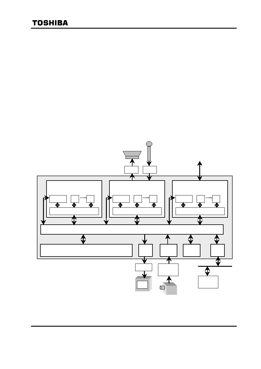
configuration.
Fig. 1 illustrates a block diagram of this LSI. Three signal processing core, peripheral interfaces,
and 12-Mbit DRAM are integrated in a single chip.
Bitstream input/output are performed via a network interface in the Mux/Demux core.
A Microphone and a speaker can be connected to a PCM interface in a speech/audio core via
external DAC and ADC.
TOSHIBA CMOS camera is connected to a camera interface via a camera DSP "TC90A50F" or
"TC90A70F". NTSC camera is also connected via an NTSC decoder.
LCD or NTSC display is connected to an LCD interface via TOSHIBA LCD controller or an NTSC
encoder, respectively.
Host CPU is connected via a host interfaces. It downloads firmwares into the embedded DRAM
and accesses to internal registers.
Fig. 1
Block Diagram
12Mbit Embedded DRAM
Arbiter + DRAM Controller
Bitstream In/Out
Cam.
I/F
LCD
I/F
Pre-
filter
Host
I/F
DMA Controller
HW
RISC
HW
MPEG-4 Video
DMA Controller
HW
RISC
HW
Speech/Audio
DMA Controller
HW
RISC
HW
Mux./Demux.
D/A
A/D
LCDC
Camera
DSP
Host
CPU
Network Bitstream
Interface
MPEG-4 Audiovisual Codec LSI
Preliminary
TC35273
TOSHIBA Confidential
2000-4-27
5/23
Version
0.90
2. Terminals
2.1 Pin Assignment
TBD
2.2 Pin Allocation
TBD
2.3 I/O Pins
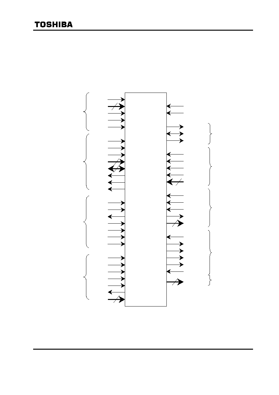
Fig. 2 Pin Map
TC35273
MPEG-4
Audiovisual
LSI
PLLDIV
PLLFN
PLLAVD
PLLBP
PLLAVS
3
/RESET
/HCS
/HWR
HADDR
/HRD
HDAT
/HWAIT
7
16
/HACK
HINT
TREOUT
TEST0-3
NWCLK
/NWOEN
NWDO
/NWIEN
NWDI
NWIFS
NWOFS
VGSADIO
VGSBDO
VGSCLK
CAMCLK
CAMHREF
CAMVREF
CAMFSEL
CAMPIXEL
DISPCLK
DISPHSYNC
DISPYSYNC
DISPBLK
DISPPIXEL
ADIMCLK
ADOMCLK
ADLRCLK
ADSCLK
ADSDO
ADSDI
ADCMD
PLL Pins
Host
Interface
Test Pins
Network
Interface
Camera
Interface
Video
General
Interface
Display
Interface
Audio
PCM
Interface
Audio
ADC&DAC
Control
STANDBY
8
8
TGCLK
TSMODE
TDBISTEN
TDTMB
TDTCLK
5
4
MPEG-4 Audiovisual Codec LSI
Preliminary
TC35273
TOSHIBA Confidential
2000-4-27
6/23
Version
0.90
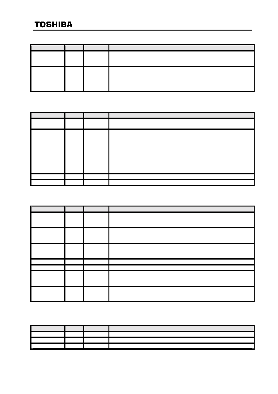
Table 1. System Control Signals
Signal Name
In/Out
Bit Width
Description
/RESET
In
1
System Reset Input (Low Active). When the LSI is reset, the reset pin has
to be low for more than 16 clock cycles. When power on, the LSI has to be
reset after PLL locked. It takes approximately 100us until the PLL locked.
STANDBY
In
1
System Standby Input (High Active).
When it is high, power is not supplied to the internal logic, SRAM, and
DRAM.
"0": Normal Operation.
"1": Standby.
Table 2. PLL Control Signals
Signal Name
In/Out
Bit Width
Description
PLLFN
In
1
Reference Clock Input.
It has to be 13.00MHz to 20MHz with +/- 10% duty.
PLLDIV[2:0]
In
3
System clock frequency select. System Clock = PLLFN * N.
"000": N=2.5.
"001": N=3.0.
"010" : N=3.5
"011": N=4.0.
"100": N=4.5.
"101": N=5:0.
"110": N=5.5.
"111": N=6.0.
PLLAVD
In
1
Analog PLL Power (VDD).
PLLAVS
In
1
Analog PLL Ground (VSS).
Table 3. Host Interface
Signal Name
In/Out
Bit Width
Description
/HCS
In
1
Chip enable input (low active).
"0" : Chip select.
"1" : Non operation.
/HWR
In
1
Write strobe (low active).
"0" : Write operation.
"1" : Non operation.
/HRD
In
1
Read Strobe (low active).
"0" : Read operation.
"1" : Non operation.
HADDR[6:0] In 7
Address
signal.
HDAT[15:0] In/Out
16
Data
signal.
HWAIT
Out
1
Bus wait signal (low active).
"0" : Wait.
"1" : Non wait.
HINT
Out
1
Interrupt signal (high active).
"0" : Non operation.
"1" : Interrupt operation.
Table 4 Video General Serial Interface
Signal Name
In/Out
Bit Width
Description
VGSCLK
Out
1
General I/F clock output. Please open unless this interface is used.
VGSADIO
In/Out
1
Input/output of serial data on port A. Open unless this interface is used.
VGSBDO
Out
1
Output of serial data on port B. Open unless this interface is used.

MPEG-4 Audiovisual Codec LSI
Preliminary
TC35273
TOSHIBA Confidential
2000-4-27
7/23
Version
0.90
MPEG-4 Audiovisual Codec LSI
Preliminary
TC35273
TOSHIBA Confidential
2000-4-27
8/23
Version
0.90
Table 5 Video Camera Interface
Signal Name
In/Out
Bit Width
Description
CAMCLK
In
1
Clock signal from camera.
CAMHREF
In
1
HREF signal from camera.
CAMVREF
In
1
VREF signal from camera.
CAMFSEL
In
1
Field select signal from camera in an NTSC mode.
CAMPIXEL
In
8
Luminance and chrominance data from camera.
Table 6 Video Display Interface
Signal Name
In/Out
Bit Width
Description
DISPCLK
In
1
Clock signal from display.
/DISPHSYNC
In
1
HSYNC signal from display.
/DISPVSYNC
In
1
VSYNC signal form display.
/DISPBLK
Out
1
Blanking signal to display.
DISPPIXEL
Out
8
Luminance (Y) and chrominance (Cb,Cr) signal output.
Table 7 Audio ADC&DAC Interface
Signal Name
In/Out
Bit Width
Description
ADOMCLK
Out
1
Master clock to external ADC/DAC chips.
ADIMCLK
In
1
Master clock from external ADC/DAC chips.
ADLRCLK
Out
1
Input/output channel clock to external ADC/DAC chips.
ADSCLK
Out
1
Audio serial data clock to external ADC/DAC chips.
ADSDI
In
1
Audio serial data input.
ADSDO
Out
1
Audio serial data output.
Table 8 Audio ADC&DAC Control Interface
Signal Name
In/Out
Bit Width
Description
ADCMD[4:0]
Out
5
Command to external ADC/DAC chips.
Table 9 Network Bit Stream Interface
Signal Name
In/Out
Bit Width
Description
NWCLK In
1 Network
clock.
/NWOEN
In
1
Network bit serial output enable.
/NWDO
Out
1
Network bit serial output data.
/NWIEN
In
1
Network bit serial input enable.
NWDI
In
1
Network bit serial input data.
NWIFS
In
1
Word synchronization for input data in the frame mode.
NWOFS
In
1
Word synchronization for output data in the frame mode.
NWINT
In
1
Frame signal input in the frame mode.
MPEG-4 Audiovisual Codec LSI
Preliminary
TC35273
TOSHIBA Confidential
2000-4-27
9/23
Version
0.90
Table 10 Test Control Signal
Signal Name
In/Out
Bit Width
Description
TGCLK
In
1
Test terminal. Please connect to Vss.
TSMODE
In
1
Test terminal. Please connect to Vss.
TDBISTEN
In
1
Test terminal. Please connect to Vss.
TREOUT
Out
1
Test terminal. Please connect to open.
TDTMB
In
1
Test terminal. Please connect to Vss.
TDTCLK
In
1
Test terminal. Please connect to Vss.
TEST[2:0]
In
3
Test terminal. Please connect to Vss.
Table 11 Power
Supply
and
GND
Signal Name
In/Out
Bit Width
Description
Vss
GND
Vdds
3.3V
Vdd
Vdd2
2.5V
Vdd
MPEG-4 Audiovisual Codec LSI
Preliminary
TC35273
TOSHIBA Confidential
2000-4-27
10/23
Version
0.90
3. Interface Specifications
3.1 Host Interface
An external host CPU accesses to TC35273 via a host interface. The access timing of a read, a
write, and an interrupt operation are explained below. The host interface has two access modes; a
handshake access mode and a synchronized access mode.
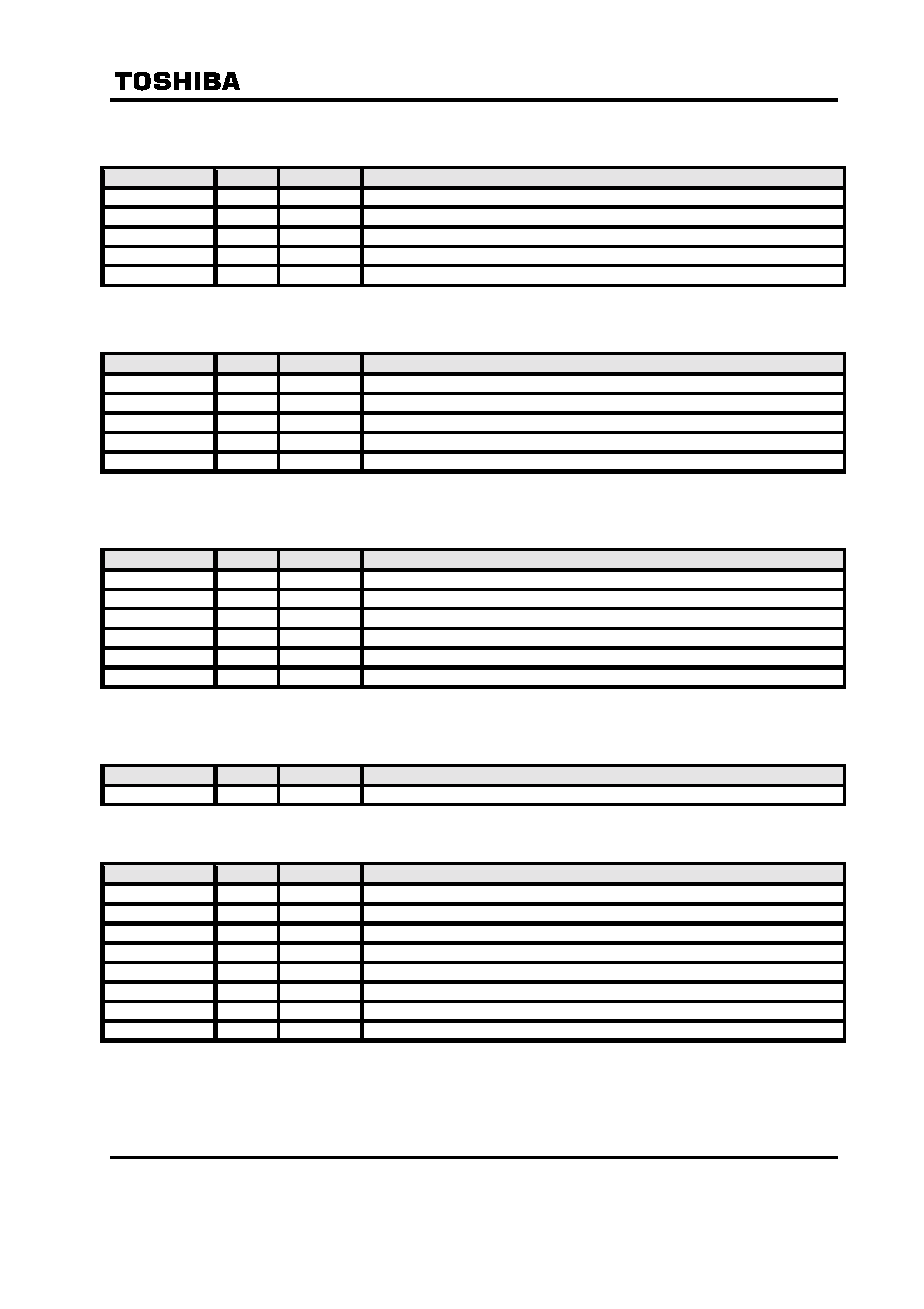
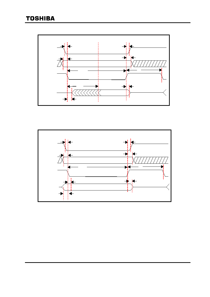
3.1.1 Handshake access mode
In this mode, the host CPU has to finish an access operation after a waiting signal (/HWAIT)
becomes high.
Fig.3 shows the timing diagram of a read operation. A read access starts by asserting both a chip
select signal (/HCS) and a read signal (/RD) (timing (a)). At this timing, /HWAIT becomes low. When
the read data are ready, /HWAIT becomes high (timing (b)). The host CPU gets the read data and
finishes the read operation by negating both /HCS and /HRD (timing (c)).
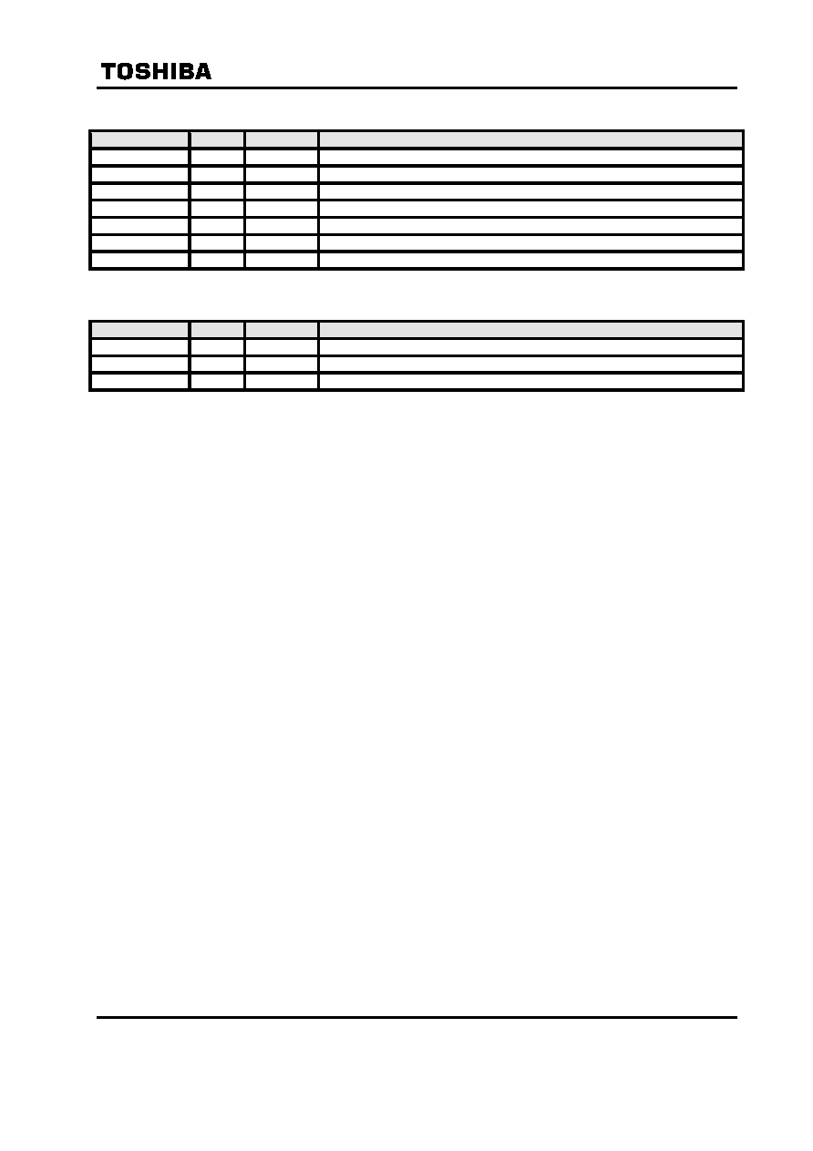
Fig.4 shows the timing diagram of a write operation. A write access starts by asserting both /HCS
and a write signal (/WR) (timing (a)). At this timing, /HWAIT becomes low. When TC35273 gets the
write data, /HWAIT becomes high (timing (b)). After that, the host CPU finishes the write operation by
negating both /HCS and /HWR (timing (c)).
Fig. 3 Read Operation in handshake mode
HADDR
/HRD
HDAT
/HWAIT
/HCS
T
CSS
T
WTAD
T
DTOD
T
DTVD
T
DTRS
T
DTID
T
RDH
T
RR
T
ADH
T
WTID
T
ADS
T
CSH
(a)
(b)
(c)
MPEG-4 Audiovisual Codec LSI
Preliminary
TC35273
TOSHIBA Confidential
2000-4-27
11/23
Version
0.90
Fig. 4 Write Operation in handshake mode
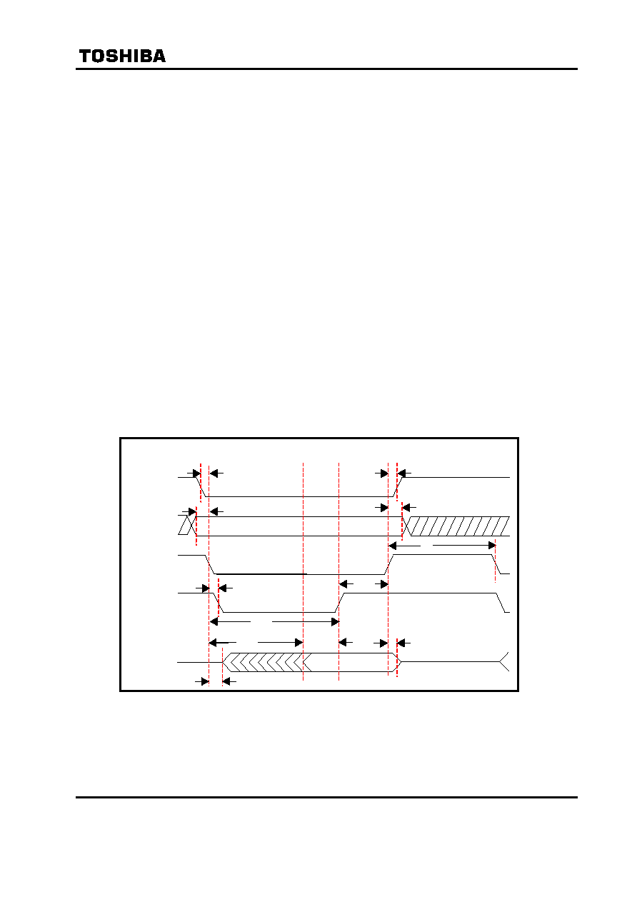
3.1.2 Synchronized access mode
In this mode, a host CPU accomplishes an access to TC35273 in the specified period without a
handshake. However, when the host CPU accesses to the embedded DRAM in TC35273, it has to
check whether the next access is available or not by checking a status register before the access.
Fig.5 shows the timing diagram of a read operation. A read access starts by asserting both a chip
select signal (/HCS) and a read signal (/RD) (timing (a)). After the specified cycles indicated as Tacs,
the host CPU gets the read data and finishes the read operation by negating both /HCS and /HRD
(timing (b)).
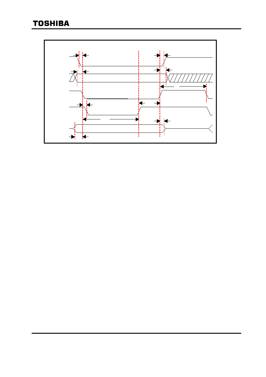
Fig.6 shows the timing diagram of a write operation. A write access starts by asserting both /HCS
and a write signal (/WR) (timing (a)). After the specified cycles, the host CPU finishes the write
operation by negating both /HCS and /HWR (timing (b)).
HADDR
/HWR
HDAT
/HWAIT
/HCS
T
CSS
T
WTAD
T
DTWS
T
DTID
T
RDH
T
RR
T
ADH
T
WTID
T
ADS
T
CSH
(a)
(b)
(c)
MPEG-4 Audiovisual Codec LSI
Preliminary
TC35273
TOSHIBA Confidential
2000-4-27
12/23
Version
0.90
Fig.5 Read Operation in Synchronization mode
Fig.6 Write Operation in Synchronization Mode
HADDR
/HRD
HDAT
/HCS
T
CSS
T
WTAD
T
DTOD
T
DTVD
T
DTRS
T
DTID
T
RDH
T
RR
T
ADH
T
ADS
T
CSH
(a)
(b)
T
ACS
HADDR
/HWR
HDAT
/HCS
T
CSS
T
WTAD
T
DTWS
T
DTID
T
RR
T
ADH
T
ADS
T
CSH
(a)
(c)
T
ACS
MPEG-4 Audiovisual Codec LSI
Preliminary
TC35273
TOSHIBA Confidential
2000-4-27
13/23
Version
0.90
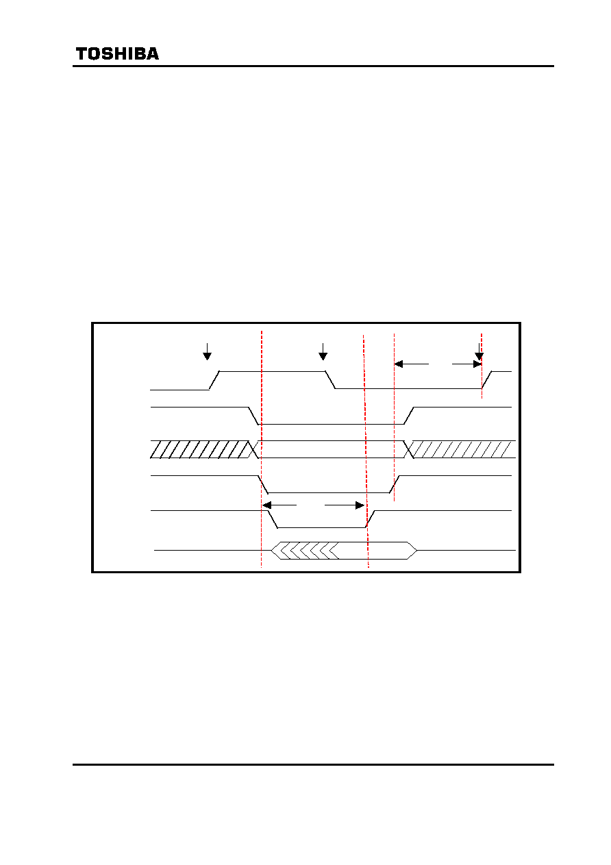
3.1.3 Interrupt
An interrupt to the external host CPU is performed as follows.
(a) HINT Active
When an interrupt is requested by TC35273, HINT becomes high (timing (a)).
(b) Clear HINT
The host CPU detects the interrupt request by HINT. The CPU also detects the interrupt
causes by reading an interrupt status register in the host interface of TC35273. When the CPU
reads the register at the timing (b), The CPU detects the interrupt causes occurring during the
timing (a) and (b). HINT is cleared when the CPU reads the interrupt status register.
(c) Multiple Interrupt
Even if another interrupt is requested during the timing (b) and (c), The assertion of HINT is
suspended to the timing (c).
Fig. 7 Interrupt Operation
HADDR
/HRD
HDAT
/HWAIT
HINT
T
RR
D
/HCS
T
ACS
(a)
(b)
(c)
MPEG-4 Audiovisual Codec LSI
Preliminary
TC35273
TOSHIBA Confidential
2000-4-27
14/23
Version
0.90
Table 12 Host Interface Timing
Parameters
Description
Min
Max
Unit
T
CSS
Setup time of HCS.
0.0
ns
T
CSH
Hold time of HCS.
0.0
ns
T
ADS
Setup time of Address.
0.0
ns
T
ADH
Hold time of Address.
0.0
ns
T
WTAD
Delay time of /HWAIT for /HRD or /HWR.
15.0
ns
T
WTID
Access time in handshake access mode.*
T
SYSCLK
*3
T
SYSCLK
*100 ns
T
ACS
Access time in synchronized access mode.
T
SYSCLK
*3
ns
T
ACID
Delay time of HACK
15.0 ns
T
DTOD
Delay time of Data.
15.0
ns
T
DTVD
Data hold time.
T
SYSCLK
*2
T
SYSCLK
*99 ns
T
DTRS
Read data setup time.
T
SYSCLK
*1 ns
T
DTwS
Write data setup time.
0.0
ns
t
DTID
Data hold time.
15.0
ns
T
RDH
Hold time of /HRD.
0.0
ns
T
RR
Recovery time of /HRD or /HWR
T
SYSCLK
*3 ns
* T
SYSCLK
means the cycle time of TC35274 internal system clock.
* Access to internal DRAM requires Tsysclk*100 (ns) in a worst case. As for the others accesses, it
takes 3 cycles of the internal system clock.
MPEG-4 Audiovisual Codec LSI
Preliminary
TC35273
TOSHIBA Confidential
2000-4-27
15/23
Version
0.90
3.2 Video General Serial Interface
This interface is reserved to control an external camera or an LCD. It is not supported now.
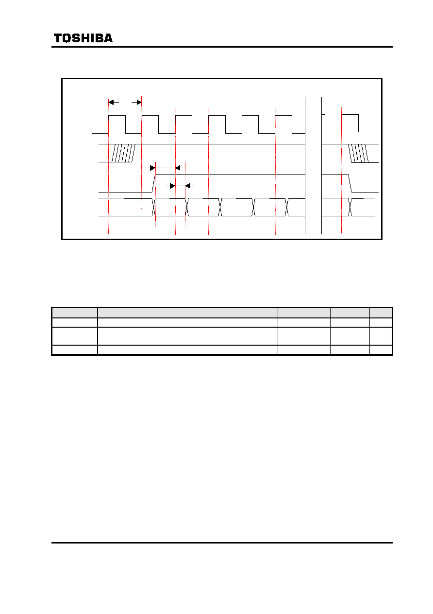
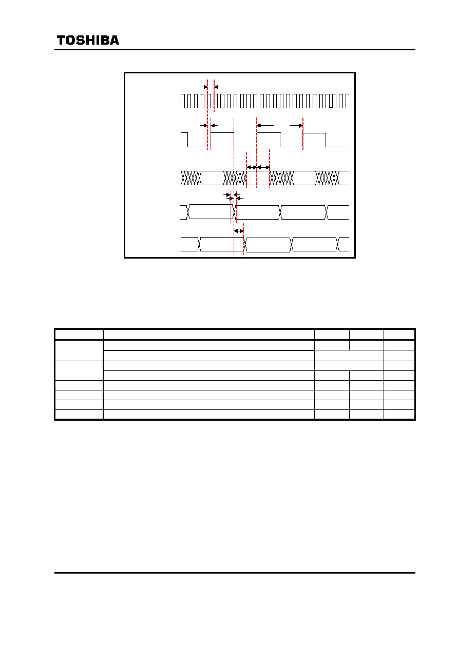
3.3 Video Camera Interface
A CMOS Camera or a CCD Camera is connected via Toshiba CMOS camera
DSP "TC90A50F" or "TC90A70F", or an ordinary NTSC decoder LSI. Fig.6, 7, 8 shows the
timing diagrams of the camera signal input. When an NTSC decoder is used, TC35273
captures either an odd field or an even field by using CAMFSEL.
Fig. 8 Frame Based CAMVREF Timing Diagram
Fig. 9 Field Based (NTSC) CAMVREF Timing Diagram
CAMHREF
CAMPIXL
CAMVREF
CAMVREF
CAMHREF
CAMFSEL
1st Field (Even Field)
2nd Field (Odd Field)
CAMPIXL
MPEG-4 Audiovisual Codec LSI
Preliminary
TC35273
TOSHIBA Confidential
2000-4-27
16/23
Version
0.90
Fig. 10 Camera Interface Timing Diagram
Table 13 Camera Interface Timing
Parameter
Description
Min
Max
Unit
T
CYCLE
Clock cycle of CAMCLK (up to 27MHz)
35
ns
T
SETUP
Setup time of CAMVREF, CAMHREF, CAMPIXEL
(T
SYSCLK
*1)+
2
ns
T
HOLD
Hold time of CAMVREF, CAMHREF, CAMPIXL
2
ns
CAMHREF
CAMVREF
CAMPXL
CAMCLK
Cb0
Cr0
Y0
Y1
T
SETUP
T
HOLD
T
CYCLE
Y n-1
MPEG-4 Audiovisual Codec LSI
Preliminary
TC35273
TOSHIBA Confidential
2000-4-27
17/23
Version
0.90
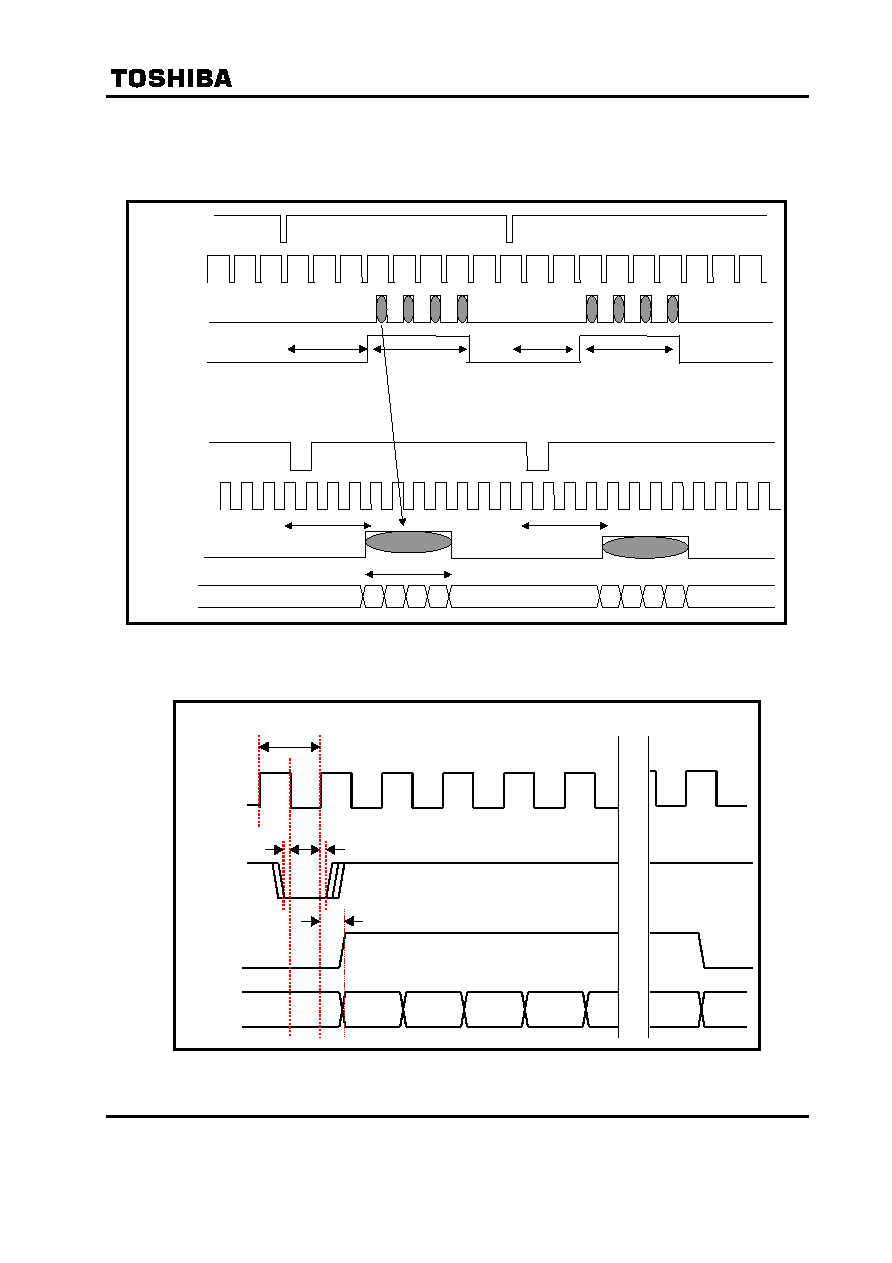
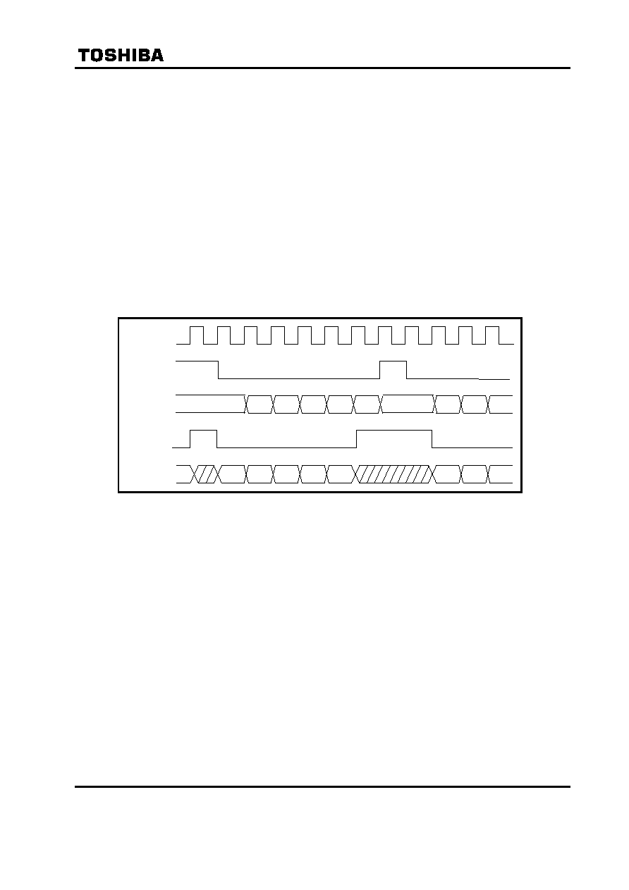
3.4 Video Display Interface
The video display interface outputs image data with YCbCr 4:2:2 8-bit digital format. An external
LCD controller is required for the connection to an LCD or a monitor.
Fig. 11 Timing Diagram of Display Interface.
Fig. 12 Detail Timing Diagram of Display Interface.
/DISPVSYN
Internal Signal
L2VBUSY
1
Cb0
/DISPHSYN
2
3
1
2
3
/DISPBLNK
Vblank=3
VSize=4
VBlank=3
VSize=4
/DISPHSYN
DISPCLK
/DISPBLNK
DISPPIXEL[7:0]
Hblank=4
HSize=2
Hblank=4
Y0 Cr0 Y1
Cb0 Y0 Cr0Y1
DSPBLK
DSPHSYN
DSPVSYN
DSPPXL
DSPCLK
Cb0
Cr0
Y0
Y1
T
SETUP
T
HOLD
T
CYCLE
Y n-1
T
DELAY
MPEG-4 Audiovisual Codec LSI
Preliminary
TC35273
TOSHIBA Confidential
2000-4-27
18/23
Version
0.90
Table 14 Display Interface Timing
Parameter
Description
Min
Max
Unit
T
CYCLE
Cycle time of DISPCLK
100
ns
T
SETUP
Setup time of DISPHSYN and DISPVSYN
2
ns
T
HOLD
Hold time DISPHSYN and DISPVSYN
2
ns
T
DELAY
Delay time of DISPBLK and DISPPXL
(T
SYSCLK
*3)+15 ns
*
When system clock is 40MHz, DSPCLK has to be less than 10MHz.
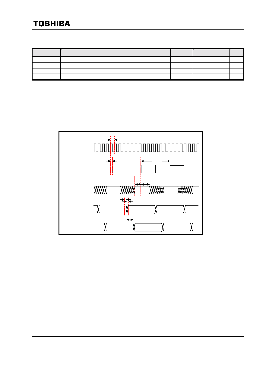
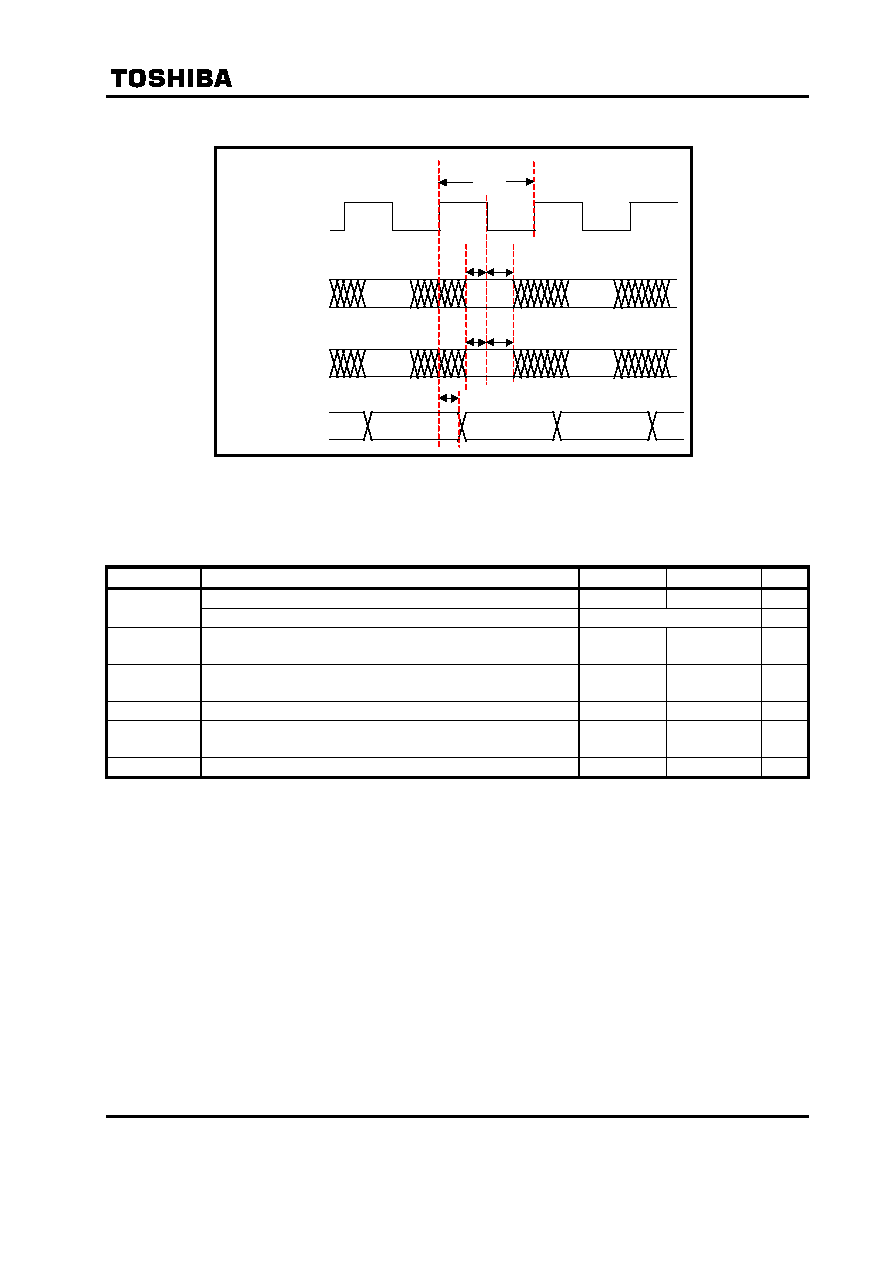
3.5 Audio ADC&DAC Interface
Asani-kasei "AK4158" and "AK4323" are connected for external ADC and DAC, respectively.
Fig. 13 Audio ADC&DAC Interface
ADSCLK
ADSDI
ADLRCLK
ADSDO
T
SCKW
T
SDIS
T
SDIH
T
SDOD
ADOMCLK
T
MCKW
T
SCKD
T
LCKD
H
T
LCKD
H
MPEG-4 Audiovisual Codec LSI
Preliminary
TC35273
TOSHIBA Confidential
2000-4-27
19/23
Version
0.90
Fig. 14 Audio ADC&DAC Interface (Master clock output mode).
Table 15 Audio ADC&DAC Interface Timing (Master clock output mode).
Parameter Description Min
Max
Unit
Clock cycle period of ADOMCLK.
80
ns
T
MCKW
Duty ratio of ADOMCLK.
50+/-10
%
Clock cycle period of ADSCLK.
T
MCKW
*8 ns
T
SCKW
Delay time from ADOMCLK to ADKCLK.
T
SYSCLK
*2
ns
T
SDIS
Setup time of ADSDI.
T
SYSCLK
*1 ns
T
SDIH
Hold time of ADSDI.
T
SYSCLK
*4 ns
T
LCKD
Delay time from ADSCLK to ADLRLCK.
T
SYSCLK
*1
ns
T
SDOD
Delay time from ADSCLK to ADSDO.
T
SYSCLK
*6
ns
ASCLK
ALRCK
ASDTI
ASDTO
15
16 Clock Cycles
14
13
12
11
1
0
15
14
13
12
11
1
0
0
0
15
15
14
14
13
13
Rch Data
Lch Data
MPEG-4 Audiovisual Codec LSI
Preliminary
TC35273
TOSHIBA Confidential
2000-4-27
20/23
Version
0.90
Fig. 15 Audio ADC&DAC Interface (Master clock input mode).
Table 16 Audio ADC&DAC Interface Timing (Master clock input mode).
Parameter Description Min
Max
Unit
Cycle time of ADIMCLK.
80
ns
T
MCKW
Duty ratio of ADIMCLK.
50
±
10
%
Cycle time of ADSCLK.
T
MCKW
*8 ns
T
SCKW
Delay time from ADIMCLK to ADSCLK.
T
SYSCLK
*3
ns
T
SDIS
Setup time of ADSDI.
T
SYSCLK
*1 ns
T
SDIH
Hold time of ADSDI.
T
SYSCLK
*4 ns
T
LCKD
Delay time from ADSCLK to ADLRLCK.
T
SYSCLK
*1
ns
T
SDOD
Delay time from ADSCLK from ADSDO.
T
SYSCLK
*6
ns
ADSCLK
ADSDI
ADLRCLK
ADSDO
T
SCKW
T
SDIS
T
SDIH
T
SDOD
ADIMCLK
T
MCKW
T
SCKD
T
LCKD
H
T
LCKD
H
MPEG-4 Audiovisual Codec LSI
Preliminary
TC35273
TOSHIBA Confidential
2000-4-27
21/23
Version
0.90
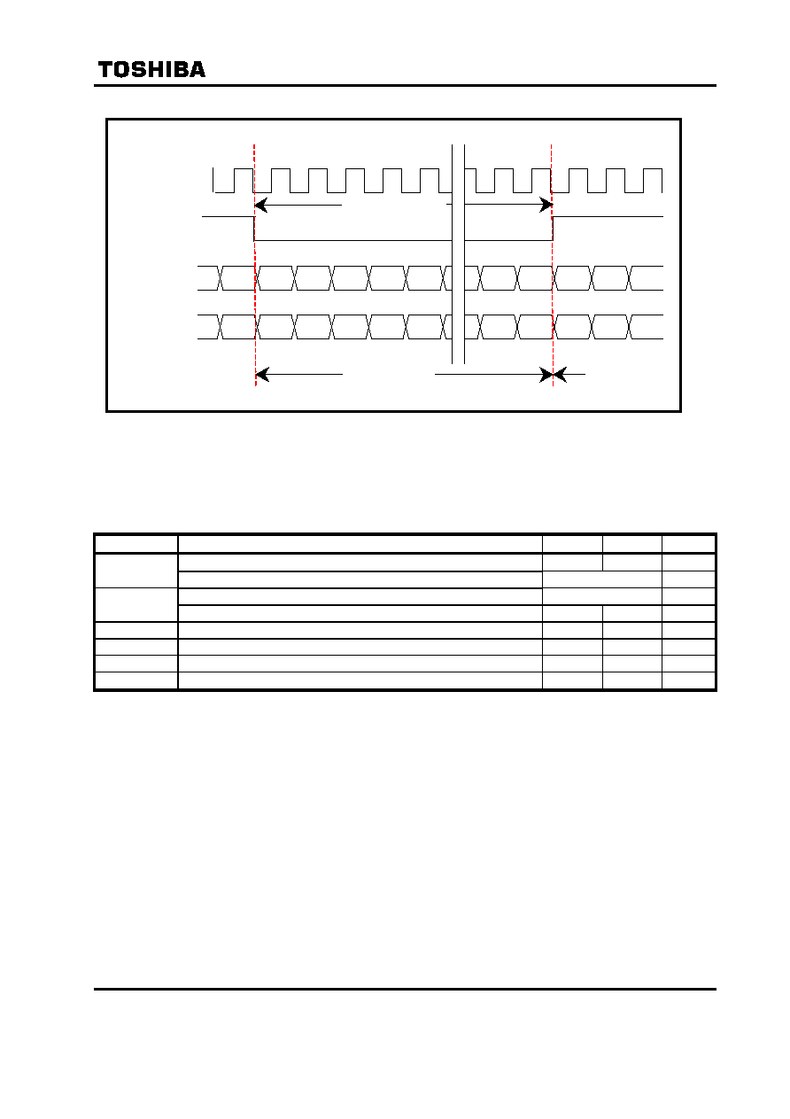
3.6 Network Bit Stream Interface
The multiplexed audiovisual bitstream data are transferred to/from a baseband LSI via a network
bit stream interface. This is full-dupulex interface and has two operation modes; a bit serial mode
and a frame mode.
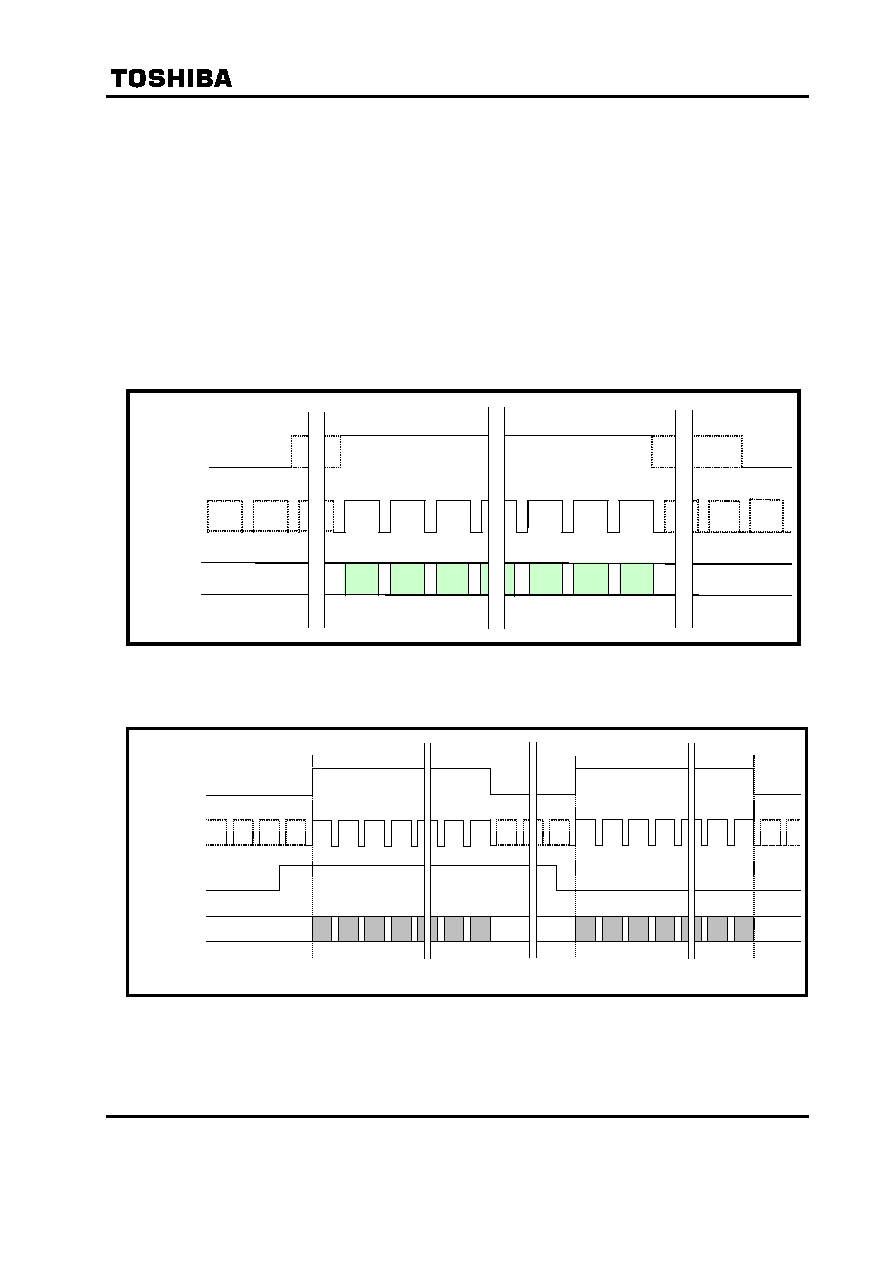
(1) Bit Serial Mode
Serial data are transferred when an enable signal indicates the data validity. In this mode, frame
and synchronization informations are contained in the transferred data.
TC35273 receives the transferred data via the NWDI pin at the negedge of the network clock
"NWCLK" if the input enable signal "NWIEN" shows the data validity. (When NWIEN is low, the data
are valid.) TC35273 also sends the data via the NWDO pin at the posedge of NWCLK if the output
enable signal "NWOEN" is high.
Fig. 16
Network bit stream timing diagram
(bit serial mode).
(2) Frame Mode
The data are transferred in accordance with both a frame signal "NWINT" and a word
synchronization signal. "NWIFS" and "NWOFS" are used for the word synchronization in the data
receive and the data send, respectively. After NWIFS or NWOFS becomes high, 16-bit data are
transferred. When the data transfer is finished in the frame, NWIFS or NWOFS does not becomes
high. In this case, the output data are fixed to low, and the input data are ignored.
NWCLK
/NWOEN
NWDO
NWDI
/NWIEN
D1
D2 D3
D4 D5
D6
D7 D8
D9
D0
D1
D2
D3
D4
D5
D6
D7
D8
D0
MPEG-4 Audiovisual Codec LSI
Preliminary
TC35273
TOSHIBA Confidential
2000-4-27
22/23
Version
0.90
Fig. 17
Network bit stream timing diagram
(frame mode).
NWCLK
NWIFS
NWDI
D14
D2
D1
D0
D15
D15
D14
D2
D1
D0 D15
NWOFS
NWDO
D3
D2
D1
D0
D15
D15
D3
D2
D1
D0
NWINT
NWCLK
NWIFS
NWDI
NWOFS
NWDO
MPEG-4 Audiovisual Codec LSI
Preliminary
TC35273
TOSHIBA Confidential
2000-4-27
23/23
Version
0.90
Fig. 18 indicates the detail timing diagram of the network bitstream interface.
Fig. 18 Detailed Network Bit Stream Interface.
Table 17 Network bit stream timing.
Parameter Description
Min
Max
Unit
Cycle time of NWCLK.
1000
ns
T
SCKW
Duty ratio of NWCLK.
50+/-10
%
T
ENS
Setup time of /NOWEN,/NWIEN, /NWINT, NWOFS,
and NWIFS
T
SYSCLK
*3 ns
T
ENH
Hold time of /NOWEN,/NWIEN, /NWINT, NWOFS,
and NWIFS
T
SYSCLK
*1
2
ns
T
SDIS
Setup time of NWDI
T
SYSCLK
*3 ns
T
SDIH
Hold time of NWDI
T
SYSCLK
*1
2
ns
T
SDOD
Delay time from NWCLK to NWDO
T
SYSCLK
*12 ns
T
SYSCLK
is the cycle time of the internal clock in TC35273.
4. Electric Specifications
4.1 TBD.
,
NWCLK
/NWOEN
/NWIEN
/NWINT
NWOFS
NWIFS
NWDI
NWDO
T
SCKW
T
ENH
T
ENS
T
SDIH
T
SDIS
T
SDOD
Document Outline