Äîêóìåíòàöèÿ è îïèñàíèÿ www.docs.chipfind.ru
TOSHIBA
TC551001BPL/BFL/BFTL/BTRL-70L/85L
TOSHIBA AMERICA ELECTRONIC COMPONENTS, INC
.
1
PIN NO.
1
2
3
4
5
6
7
8
9
10
11
12
13
14
15
16
PIN NAME
A
11
A
9
A
8
A
13
R/W
CE2
A
15
V
DD
NC
A
16
A
14
A
12
A
7
A
6
A
5
A
4
PIN NO.
17
18
19
20
21
22
23
24
25
26
27
28
29
30
31
32
PIN NAME
A
3
A
2
A
1
A
0
I/O1
I/O2
I/O3
GND
I/O4
I/O5
I/O6
I/O7
I/O8
CE1
A
10
OE
Features
· Low power dissipation
:
27.5mW/MHz (typ.)
· Standby current:
4
µ
A (max.) at Ta = 25
°
C
· 5V single power supply
· Access time (max.)
· Power down feature:
CE1, CE2
· Data retention supply voltage:
2.0 ~ 5.5V
· Inputs and outputs directly TTL compatible
· Package
TC551001BPL
: DIP32-P-600
TC551001BFL :
SOP32-P-525
TC551001BFTL
: TSOP32-P-0820
TC551001BTRL
: TSOP32-P-0820A
TC551001BPL/BFL/BFTL/BTRL
-70L
-85L
Access Time
70ns
85ns
CE1 Access Time
70ns
85ns
CE2 Access Time
70ns
85ns
OE Access Time
35ns
45ns
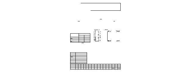
Pin Connection (Top View)
TSOP Pinout
SILICON GATE CMOS
131,072 WORD x 8 BIT STATIC RAM
Description
The TC551001BPL is a 1,048,576 bits static random access memory organized as 131,072 words by 8 bits using CMOS technology,
and operated from a single 5V power supply. Advanced circuit techniques provide both high speed and low power features with an
operating current of 5mA/MHz (typ.) and a minimum cycle time of 70ns. When CE1 is a logical high, or CE2 is low, the device is
placed in a low power standby mode in which the standby current is 2
µ
A typically. The TC551001BPL has three control inputs.
Chip Enable inputs (CE1, CE2) allow for device selection and data retention control, while an Output Enable input (OE) provides fast
memory access. The TC551001BPL is suitable for use in microprocessor application systems where high speed, low power, and
battery backup are required.
The TC551001BPL is offered in a standard dual-in-line 32-pin plastic package, a small outline plastic package, and a thin small
outline plastic package (forward, reverse type).
Pin Names
A0 ~ A16
Address Inputs
R/W
Read/Write Control Input
OE
Output Enable Input
CE1, CE2
Chip Enable Inputs
I/O1 ~ I/O8
Data Input/Output
V
DD
Power (+5V)
GND
Ground
N.C.
No Connection
TC551001BPL/BFL/BFTL/BTRL-70L/85L
Static RAM
SR01020795
2
TOSHIBA AMERICA ELECTRONIC COMPONENTS, INC
.
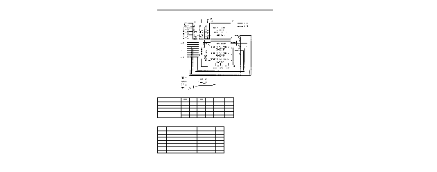
Block Diagram
* H or L
Maximum Ratings
* -3.0V at pulse width of 50ns Max
** SOP
Operating Mode
OPERATION MODE
CE1
CE2
OE
R/W
I/O1 ~ I/O8
POWER
Read
L
H
L
H
D
OUT
I
DDO
Write
L
H
*
L
D
IN
I
DDO
Output Deselect
L
H
H
H
High-Z
I
DDO
Standby
H
*
*
*
High-Z
I
DDS
*
L
*
*
High-Z
I
DDS
SYMBOL
ITEM
RATING
UNIT
V
DD
Power Supply Voltage
-0.3 ~ 7.0
V
V
IN
Input Voltage
-0.3* ~ 7.0
V
V
I/O
Input and Output Voltage
-0.5 ~ V
DD
+ 0.5
V
P
D
Power Dissipation
1.0/0.6**
W
T
SOLDER
Soldering Temperature (10s)
260
°
C
T
STRG
Storage Temperature
-55 ~ 150
°
C
T
OPR
Operating Temperature
0 ~ 70
°
C
SR01020795
Static RAM
TC551001BPL/BFL/BFTL/BTRL-70L/85L
TOSHIBA AMERICA ELECTRONIC COMPONENTS, INC
.
3
* -3.0V at pulse width of 50ns Max.
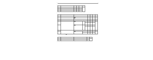
DC and Operating Characteristics (Ta = 0 ~ 70ºC, V
DD
= 5V
±
10%)
Note: (1) In standby mode with CE1
V
DD
- 0.2V, these specification limits are guaranteed under the condition of CE2
V
DD
- 0.2V or CE2
0.2V.
Note: This parameter is periodically sampled and is not 100% tested.
DC Recommended Operating Conditions
SYMBOL
PARAMETER
MIN.
TYP.
MAX.
UNIT
V
DD
Power Supply Voltage
4.5
5.0
5.5
V
V
IH
Input High Voltage
2.2
V
DD
+ 0.3
V
IL
Input Low Voltage
-0.3*
0.8
V
DH
Data Retention Supply Voltage
2.0
5.5
SYMBOL
PARAMETER
TEST CONDITION
MIN.
TYP.
MAX.
UNIT
I
LI
Input Leakage Current
V
IN
= 0 ~ V
DD
±
1.0
µ
A
I
LO
Output Leakage Current
CE1 = V
IH
or CE2 = V
IL
or R/W = V
IL
or
OE = V
IH,
V
OUT
= 0 ~ V
DD
±
1.0
µ
A
I
OH
Output High Current
V
OH
= 2.4V
-1.0
mA
I
OL
Output Low Current
V
OL
= 0.4V
4.0
mA
I
DDO1
Operating Current
CE1 = V
IL
and CE2 = V
IH
and R/W = V
IH,
I
OUT
= 0mA
Other Inputs = V
IH
/V
IL
t
cycle
Min.
70
mA
1
µ
s
20
I
DDO2
CE1 = 0.2V and
CE2 = V
DD
- 0.2V
R/W = V
DD
- 0.2V
I
OUT
= 0mA
Other Inputs
= V
DD
- 0.2V/0.2V
t
cycle
Min.
60
1
µ
s
10
I
DDS1
Standby Current
CE1 = V
IH
or CE2 = V
IL
3
mA
I
DDS2
(1)
CE1 = V
DD
- 0.2V or
CE2 = 0.2V
V
DD
= 2.0V ~ 5.5V
Ta = 0 ~ 70
°
C
30
µ
A
Ta = 25
°
C
2
4
Capacitance (Ta = 25ºC, f = 1MHz)
SYMBOL
PARAMETER
TEST CONDITION
MAX.
UNIT
C
IN
Input Capacitance
V
IN
= GND
10
pF
C
OUT
Output Capacitance
V
OUT
= GND
10
TC551001BPL/BFL/BFTL/BTRL-70L/85L
Static RAM
SR01020795
4
TOSHIBA AMERICA ELECTRONIC COMPONENTS, INC
.
AC Characteristics (Ta = 0 ~ 70
°
C, V
DD
= 5V
±
10%)
Read Cycle
Write Cycle
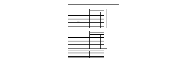
AC Test Conditions
SYMBOL
PARAMETER
TC551001BPL/BFL/BFTL/BTRL
UNIT
-70L
-85L
MIN.
MAX.
MIN.
MAX.
t
RC
Read Cycle Time
70
85
ns
t
ACC
Address Access Time
70
85
t
CO1
CE1 Access Time
70
85
t
CO2
CE2 Access Time
70
85
t
OE
Output Enable to Output in Valid
35
45
t
COE
Chip Enable (CE1, CE2) to Output in Low-Z
10
10
t
OEE
Output Enable to Output in Low-Z
5
5
t
OD
Chip Enable (CE1, CE2) to Output in High-Z
25
30
t
ODO
Output Enable to Output in High-Z
25
30
t
OH
Output Data Hold Time
10
10
SYMBOL
PARAMETER
TC551001BPL/BFL/BFTL/BTRL
UNIT
-70L
-85L
MIN.
MAX.
MIN.
MAX.
t
WC
Write Cycle Time
70
85
ns
t
WP
Write Pulse Width
50
60
t
CW
Chip Selection to End of Write
60
75
t
AS
Address Setup Time
0
0
t
WR
Write Recovery Time
0
0
t
ODW
R/W to Output in High-Z
25
30
t
OEW
R/W to Output in Low-Z
5
5
t
DS
Data Setup Time
30
35
t
DH
Data Hold Time
0
0
Input Pulse Levels
2.4V/0.6V
Input Pulse Rise and Fall Time
5ns
Input Timing Measurement Reference Level
1.5V
Output Timing Measurement Reference Level
1.5V
Output Load
1 TTL Gate and C
L
= 100pF

SR01020795
Static RAM
TC551001BPL/BFL/BFTL/BTRL-70L/85L
TOSHIBA AMERICA ELECTRONIC COMPONENTS, INC
.
5
Timing Waveforms
Read Cycle
(1)
Write Cycle 1
(4)
(R/W Controlled Write)

TC551001BPL/BFL/BFTL/BTRL-70L/85L
Static RAM
SR01020795
6
TOSHIBA AMERICA ELECTRONIC COMPONENTS, INC
.
Write Cycle 2
(4)
(CE1 Controlled Write)
Write Cycle 3
(4)
(CE2 Controlled Write)

SR01020795
Static RAM
TC551001BPL/BFL/BFTL/BTRL-70L/85L
TOSHIBA AMERICA ELECTRONIC COMPONENTS, INC
.
7
Notes:
1. R/W is High for Read Cycle.
2. Assuming that CE1 Low transition or CE2 High transition occurs coincident with or after the R/W low transition, Out-
puts remain in a high impedance state.
3. Assuming that CE1 High transition or CE2 Low transition occurs coincident with or prior to the R/W high transition,
Outputs remain in a high impedance state.
4. Assuming that OE is High for a Write Cycle, Outputs are in a high impedance state during this period.
5. The I/O may be in the output state during this time, input signals of opposite phase must not be applied.

TC551001BPL/BFL/BFTL/BTRL-70L/85L
Static RAM
SR01020795
8
TOSHIBA AMERICA ELECTRONIC COMPONENTS, INC
.
Data Retention Characteristics (Ta = 0 ~ 70
°
C)
*3
µ
A (max.) Ta = 0 ~ 40
°
C
CE1 Controlled Data Retention Mode
(1)
CE2 Controlled Data Retention Mode
(3)
Notes:
1. In the CE1 controlled data retention mode, minimum standby current is achieved under the condition CE2
0.2V or
CE2
V
DD
- 0.2V.
2. If the V
IH
of CE1 is 2.2V in operation, during the period that the V
DD
voltage is going down from 4.5V to 2.4V, I
DDS1
current flows.
3. In the CE2 controlled data retention mode, minimum standby current is achieved under the condition CE2
0.2V.
SYMBOL
PARAMETER
MIN.
TYP.
MAX.
UNIT
V
DH
Data Retention Supply Voltage
2.0
5.5
V
I
DDS2
Standby Current
V
DD
= 3.0V
15*
µ
A
V
DD
= 5.5V
30
t
CDR
Chip Deselect to Data Retention Mode
0
ns
t
R
Recovery Time
5
ms

SR01020795
Static RAM
TC551001BPL/BFL/BFTL/BTRL-70L/85L
TOSHIBA AMERICA ELECTRONIC COMPONENTS, INC
.
9
Outline Drawing
DIP32-P-600
Unit in mm

TC551001BPL/BFL/BFTL/BTRL-70L/85L
Static RAM
SR01020795
10
TOSHIBA AMERICA ELECTRONIC COMPONENTS, INC
.
Outline Drawing
SOP32-P-525
Unit in mm

SR01020795
Static RAM
TC551001BPL/BFL/BFTL/BTRL-70L/85L
TOSHIBA AMERICA ELECTRONIC COMPONENTS, INC
.
11
Outline Drawing
TSOP32-P-0820
Unit in mm

TC551001BPL/BFL/BFTL/BTRL-70L/85L
Static RAM
SR01020795
12
TOSHIBA AMERICA ELECTRONIC COMPONENTS, INC
.
Outline Drawing
TSOP32-P-0820A
Unit in mm
1. This technical data may be controlled under U.S. Export Administration Regulations and may be subject to the approval of the U.S. Department of Commerce prior to export. Any export or re-export, directly or indi-
rectly, in contravention of the U.S. Export Administration Regulations is strictly prohibited.
2. LIFE SUPPORT POLICY
Toshiba products described in this document are not authorized for use as critical components in life support systems without the written consent of the appropriate officer of Toshiba America, Inc. Life support sys-
tems are either systems intended for surgical implant in the body or systems which sustain life.
A critical component in any component of a life support system whose failure to perform may cause a malfunction of the life support system, or may affect its safety or effectiveness.
3. The information in this document has been carefully checked and is believed to be reliable; however no responsibility can be assumed for inaccuracies that may not have been caught. All information in this data book
is subject to change without prior notice. Furthermore, Toshiba cannot assume responsibility for the use of any license under the patent rights of Toshiba or any third parties.

Back to Memory