 | –≠–ª–µ–∫—Ç—Ä–æ–Ω–Ω—ã–π –∫–æ–º–ø–æ–Ω–µ–Ω—Ç: TC5565APL | –°–∫–∞—á–∞—Ç—å:  PDF PDF  ZIP ZIP |
TOSHIBA MOS MEMORY PRODUCTS
TC5565APL-10, TC5565APL-12, TC5565APL-15
TC5565AFL-10, TC5565AFL-12, TC5565AFL-15
DESCRIPTION
The TC5565APL/AFL is 65,536 bit static random access memory organized as 8,192 words by 8 bits using CMOS technology, and
operates from a single 5V supply. Advanced circuit techniques provide both high speed and low power features with a maximum
operating current of 5mA/MHz and maximum access time of 100ns/120ns/150ns.
When CE2 is a logical low or \CEl is a logical high, the device is placed in low power standby mode in which standby current is 2uA
typically. The TC5565APL/AFL has three control inputs. Two chip enable (\CE1, CE2) allow for device selection and data retention
control, and an output enable input (\OE) provides fast memory access. Thus the TC5565APL/AFL is suitable for use in various
microprocessor application systems where high speed, low power, and battery back up are required.
The TC5565APL also features pin compatibility with the 64K bit EPROM (TMM2764D).
RAM and EPROM are then interchangeable in the same socket, resulting in flexibility in the definition of the quantity of RAM versus
EPROM in microprocessor application systems. The TC5565APL is offered in a dual-in-line 28 pin standard plastic package. The
TC5565AFL is offered in 28 pin mini Flat Package.
FEATURES
∑
Low Power Dissipation
27.5mW/MHz(Max.) operating
∑
Standby Current: 100uA(Max.) Ta=70∞C
∑
Access Time
TC5565APL/AFL-10 : 100ns(Max.)
TC5565APL/AFL-12 : 120ns(Max.)
TC5565APL/AFL-15 : 150ns(Max.)
∑
5V Single Power Supply -
∑
Power Down Features: CE2, \CE1
∑
Fully Static Operation
Data Retention Supply Voltage: 2.0-5.5V
∑
Directly TTL Compatible
: All
Inputs and Outputs
∑
Pin Compatible with 2764 type EPROM
∑
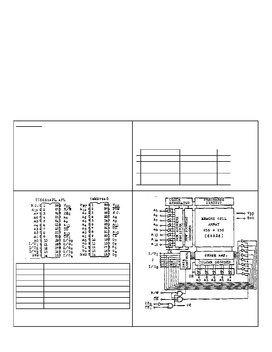
TC5565APL Family (Package Type)
Package Type Device Name
600 mil DIP TC5565APL
300 mil DIP
(Slim Package)
*TC5563APL
Flat Package
(SOP)
TC5565AFL
* See TC5563APL Technical Data.
PIN CONNECTION
(TOP VIEW)
AO-A12 Address Inputs
R/W Read/Write Control Input
\OE Output Enable Input
\CE1, CE2 Chip Enable Inputs
I/O1 ≠ I/O8 Data Input/Output
V
DD
Power (+5V)
GND Ground
N.C. No Connection
BLOCK DIAGRAM
TC5565APL-10, TC5565APL-12, TC5565APL-15
TC5565AFL-10, TC5565AFL-12, TC5565AFL-15
OPERATION MODE
\CE1
CE2
\OE
R/W
1/01-T/08
POWER
Read
L
H
L
H
D
OUT
I
DDO
Write
L
H
*
L
D
IN
I
DDO
Output Deselect
L
H
H
H
High-Z
I
DDO
H
*
*
*
High-Z
I
DDS
Standby
L
*
*
High-Z
I
DDS
MAXIMUM RATINGS
SYMBOL
ITEM
RATING
UNIT
V
DD
Power Supply Voltage
-0.3~7.0
v
V
IN
Input Voltage
*-0.3~7.0
v
V
I/O
Input and Output Voltage
-0-5-VDD+0.5
v
P
D
Power Dissipation
1.0/0.6**
W
T
solder
Soldering
Temperature
260-10
∞C sec
T
stg
Storage Temperature
-55~150
∞C
T
opr
Operating Temperature
0-70
∞C
* -3.0V
at pulse width 50ns MAX. **Flat package
D.C RECOMMENDED OPERATING CONDITIONS
SYMBOL
PARAMETER
MIN.
Typ.
MAX.
UNIT
V
DD
Power Supply Voltage
4.5
5.0
5.5
v
V
IH
Input High Voltage
2.2
-
V
DD
+0.3
v
V
IL
Input Low Voltage
-0.3
-
0.8
V
V
DH
Data-Retention Supply Voltage
2.0
-
5.5
V
TC5565APL-10, TC5565APL-12, TC5565APL-15
TC5565AFL-10, TC5565AFL-12, TC5565AFL-15
D.C and OPERATING CHARACTERISTICS (Ta=0~70
∞C
,
V
DD
= 5V±10%)
SYMBOL
PARAMETER
TEST CONDITION
MIN. TYP. MAX. UNIT
I
IL
Input Leakage
Current
V
IN=
O~V
DD
-
-
±1.0
uA
I
OH
Output High Current
VOH-2-4V
-1.0
-
mA
I
OL
Output Low Current
VOL-0.4V
4.0
-
mA
I
LO
Output Leakage Current
V
IH
or CE2-VOL or
\CE1 = V
IH
or CE2=V
OL
0r R/W = V
IL
or \OE=V
IH
V
OUT
=0~V
DD
-
-
±1.0
uA
t
cycle
=1.0us
10
mA
TC5565APL-10
TC556SAFL-10
t
cycle
=100ns
-
-
45
mA
TC5565APL-12
TC5565AFL-12
t
cycle
=120ns
-
-
40
mA
I
DDO1
V
DD
=5.5V
\CE1=V
IL
CE2=V
IH
Other input=
V
IH
/V
IL
TC5565A?L-15
TC5565AFL-15
t
cycle
=150ns
-
-
35
mA
t
cycle=1.0us
-
-
5
mA
TC5565APL-10
TC5565AFL-10
t
cycle
=100ns
-
-
40
mA
TC5565AFL-12
TC5565AFL-12
t
cycle
=120ns
-
-
35
mA
TC5565APL-15
I
DD02
Operating Current
V
DD=
5.5V
\CEl=O.2V
CE2=V
DD
≠0.2V
Other lnput=
V
DD
- 0.2V/0.2V
TC5565AFL-15
t
cycle
=150ns
-
-
30
mA
I
DDS1
\Cel = V
IH
or CE2 = V
IL
3
mA
V
DD
= 5.5V
-
2
100
uA
*I
DDS2
Standby Current
\CE1 = V
DD
≠ 0.2V or
CE2 = 0.2V
V
DD
= 3.0V
-
1
50
uA
Note * In standby mode with \CE1>= V
DD
≠ 0.2V, these specification limits are guaranteed under the condition of
CE2 >= V
DD
≠ 0.2V or CE2 <= 0.2V.
CAPACITANCE
(Ta=25
∞C
)
SYMBOL
PARAMETER
TEST CONDITION
MIN.
TYP.
MAX. UNIT
C
IN
Input Capacitance
V
IN
= GND
-
-
10
pF
C
OUT
Output Capacitance
V
OUT
= GND
-
-
10
pF
* This parameter periodically sampled is not 100% tested.

TC5565APL-10, TC5565APL-12, TC5565APL-15
TC5565AFL-10, TC5565AFL-12, TC5565AFL-15
A.C. CHARACTERISTICS
(Ta=0~70
∞C
, V
DD
= 5V±10%)
Read Cycle
SYMBOL PARAMETER
TC5565APL-10
TC5565AFL-10
TC5565APL-12
TC5565AFL-12
TC5565APL-15
TC5565AFL-15
MIN.
MAX.
MIN.
MAX.
MIN.
MAX
t
RC
Read Cycle Time
100
-
120
-
150
-
t
ACC
Address Access Time
-
100
-
120
-
150
t
COL
\CE1 Access Time
-
100
-
120
-
150
t
C02
CE2 Access Time
-
100
-
120
-
150
t
OE
Output Enable to Output Valid
-
50
-
60
-
70
t
COE
Chip Enable (\CE1, CE2) to
Output in Low-Z
10
-
10
-
15
-
t
OEE
Output Enable to Output in Low-Z
5
-
5
-
5
-
t
OD
Chip Enable (CE1, CE2) to
Output in High-Z
-
35
-
40
-
50
t
ODO
Output Enable to Output in High-Z
-
35
-
40
-
50
t
OH
Output Data Hold Time
20
-
20
-
20
-
Write Cycle
TC5565APL-10
TC5565AFL-10
TC5565APL-12
TC5565AFL-12
TC5565APL- 5
TC5565AFL- 5
SYMBOL
PARAMETER
MIN.
MAX.
MIN.
MAX.
MIN.
MAX..
t
WC
Write Cycle Time
100
-
120
-
150
-
t
WP
Write Pulse Width
60
-
70
-
90
-
t
CW
Chip Selection to End of Write
80
-
85
-
100
-
t
AS
Address Set up Time
0
-
0
-
0
-
r
WR
Write Recovery Time
0
-
0
-
0
-
t
ODW
R/W to Output High-Z
-
35
0
40
-
50
r
OEW
R/W to Output Low-Z
5
-
5
-
10
-
t
DS
Data Set up Time
40
-
50
-
60
-
t
DH
Data Hold Time
0
-
0
-
0
-
A.C. TEST CONDITION
Output Load
: 100pF + 1 TTL Gate
Input Pulse Level
: 0.6V, 2.4V
Timing Measurement
V
IN
: 0.8V, 2.2V
Reference Level
V
OUT
: 0.8V, 2.2V
t
r,
t
f
: 5ns

TC5565APL-10, TC5565APL-12, TC5565APL-15
TC5565AFL-10, TC5565AFL-12, TC5565AFL-15
TIMING WAVEFORMS
READ CYCLE (1)
WRITE CYCLE 1 (4) (R/W Controlled Write)