
TC55NEM208AFPN/AFTN55,70
2002-09-18 1/10
TENTATIVE TOSHIBA MOS DIGITAL INTEGRATED CIRCUIT SILICON GATE CMOS
524,288-WORD BY 8-BIT STATIC RAM
DESCRIPTION
The TC55NEM208AFPN/AFTN is a 4,194,304-bit static random access memory (SRAM) organized as 524,288
words by 8 bits. Fabricated using Toshiba's CMOS Silicon gate process technology, this device operates from a
single 5V
±
10% power supply. Advanced circuit technology provides both high speed and low power at an operating
current of 3 mA/MHz (typ) and a minimum cycle time of 55 ns. It is automatically placed in low-power mode at 1
µ
A
standby current (typ) when chip enable ( CE ) is asserted high. There are two control inputs. CE is used to select
the device and for data retention control, and output enable ( OE ) provides fast memory access. This device is well
suited to various microprocessor system applications where high speed, low power and battery backup are required.
And, with a guaranteed operating range of
-
40∞ to 85∞C, the TC55NEM208AFPN/AFTN can be used in
environments exhibiting extreme temperature conditions. The TC55NEM208AFPN/AFTN is available in a
standard plastic 32-pin small-outline package (SOP) and normal and reverse pinout plastic 32-pin
thin-small-outline package (TSOP).
FEATURES
∑
Low-power dissipation
Operating: 15 mW/MHz (typical)
∑
Single power supply voltage of 5 V
±
10%
∑
Power down features using CE .
∑
Data retention supply voltage of 2.0 to 5.5 V
∑
Direct TTL compatibility for all inputs and outputs
∑
Wide operating temperature range of
-
40∞ to 85∞C
∑
Standby Current (maximum):20
µ
A
PIN ASSIGNMENT
(TOP VIEW)
PIN NAMES
32 PIN SOP &
TSOP
A0~A18 Address
Inputs
R/W
Read/Write Control
OE Output
Enable
CE Chip
Enable
I/O1~I/O8 Data
Inputs/Outputs
V
DD
Power
(
+
5 V)
GND Ground
∑
Access Times (maximum):
TC55NEM208AFPN/AFTN
55 70
Access Time
55 ns
70 ns
CE Access Time
55 ns
70 ns
OE Access Time
30 ns
35 ns
∑
Package:
SOP32-P-525-1.27 (AFPN)
(Weight: g typ)
TSOP II32-P-400-1.27 (AFTN) (Weight: g typ)
1 32
2 31
3 30
4 29
5 28
6 27
7 26
8 25
9 24
10 23
11 22
12 21
13 20
14 19
15 18
16 17
V
DD
A15
A17
R/W
A13
A8
A9
A11
A10
I/O8
I/O7
I/O6
I/O5
I/O4
A18
A16
A14
A12
A7
A6
A5
A4
A3
A2
A1
A0
I/O1
I/O2
I/O3
GND
CE
OE
(AFPN/AFTN)

TC55NEM208AFPN/AFTN55,70
2002-09-18 2/10
BLOCK DIAGRAM
OPERATING MODE
MODE
CE
OE R/W
I/O1~I/O8
POWER
Read L
L
H
Output
I
DDO
Write L
*
L Input
I
DDO
Output Deselect
L
H
H
High-Z
I
DDO
Standby H
*
*
High-Z
I
DDS
*
= don't care
H = logic high
L = logic low
MAXIMUM RATINGS
SYMBOL RATING
VALUE
UNIT
V
DD
Power Supply Voltage
-
0.3~7.0 V
V
IN
Input Voltage
-
0.3
*
~7.0 V
V
I/O
Input/Output Voltage
-
0.5~V
DD
+
0.5
V
P
D
Power Dissipation
0.6
W
T
solder
Soldering Temperature (10s)
260
∞C
T
stg
Storage Temperature
-
55~150 ∞C
T
opr
Operating Temperature
-
40~85 ∞C
*
:
-
2.0 V when measured at a pulse width of 20ns
COLUMN ADDRESS
BUFFER
A5
I/O1
MEMORY CELL ARRAY
2,048
◊
256
◊
8
(4,194,304)
COLUMN ADDRESS
DECODER
COLUMN ADDERSS
REGISTER
SENSE AMP
CE
A6
A7
A8
A9
A14
A11
A15
A16
CE
V
DD
GND
CE
R/W
OE
A4
CE
A18
A2
A0 A1
A17
A3 A10 A12A13
ROW ADDRESS
DECODER
ROW ADDRESS
BUFFER
ROW ADDRESS
REG
I
STER
I/O2
I/O3
I/O4
I/O5
I/O6
I/O7
I/O8
DA
T
A
CON
T
R
O
L
CLOCK
GENERA
T
O
R
8
TC55NEM208AFPN/AFTN55,70
2002-09-18 3/10
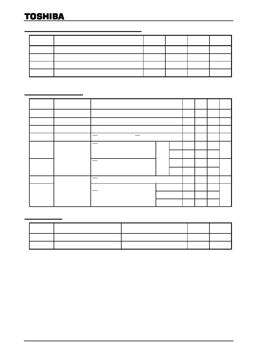
DC RECOMMENDED OPERATING CONDITIONS
(Ta
=
-
40∞ to 85∞C)
SYMBOL PARAMETER MIN TYP MAX UNIT
V
DD
Power Supply Voltage
4.5
5.0
5.5
V
V
IH
Input High Voltage
2.2
V
DD
+
0.3
V
V
IL
Input Low Voltage
-
0.3
*
0.6 V
V
DH
Data Retention Supply Voltage
2.0
5.5 V
*
:
-
2.0 V when measured at a pulse width of 20 ns
DC CHARACTERISTICS
(Ta
=
-
40∞ to 85∞C, V
DD
=
5 V
±
10%)
SYMBOL PARAMETER
TEST CONDITION
MIN
TYP
MAX
UNIT
I
IL
Input Leakage
Current
V
IN
=
0 V~V
DD
±
1.0
µ
A
I
OH
Output
High
Current
V
OH
=
2.4 V
-
1.0
mA
I
OL
Output
Low
Current
V
OL
=
0.4 V
2.1
mA
I
LO
Output Leakage
Current
CE
=
V
IH
or R/W
=
V
IL
or OE
=
V
IH
, V
OUT
=
0 V~V
DD
±
1.0
µ
A
MIN
35
l
DDO1
CE
=
V
IL
and R/W
=
V
IH
,
I
OUT
=
0 mA,
Other Input
=
V
IH
/V
IL
1
µ
s
8
mA
MIN
30
l
DDO2
Operating Current
CE
=
0.2 V and R/W
=
V
DD
-
0.2 V,
I
OUT
=
0 mA,
Other Input
=
V
DD
-
0.2 V/0.2 V
t
cycle
1
µ
s
3
mA
I
DDS1
CE
=
V
IH
3 mA
Ta
=
25∞C
1
Ta
=
-
40~40∞C
3
I
DDS2
Standby Current
CE
=
V
DD
-
0.2 V,
V
DD
=
2.0 V~5.5 V
Ta
=
-
40~85∞C
20
µ
A
CAPACITANCE
(Ta
=
25∞C, f
=
1 MHz)
SYMBOL PARAMETER
TEST CONDITION
MAX
UNIT
C
IN
Input
Capacitance
V
IN
=
GND
10
pF
C
OUT
Output
Capacitance
V
OUT
=
GND
10
pF
Note: This parameter is periodically sampled and is not 100% tested.

TC55NEM208AFPN/AFTN55,70
2002-09-18 4/10
AC CHARACTERISTICS AND OPERATING CONDITIONS
(Ta
=
-
40∞ to 85∞C, V
DD
=
5 V
±
10%)
READ CYCLE
TC55NEM208AFPN/AFTN
55 70
SYMBOL PARAMETER
MIN MAX MIN MAX
UNIT
t
RC
Read
Cycle
Time
55
70
t
ACC
Address
Access
Time
55
70
t
CO
Chip
Enable
Access
Time
55
70
t
OE
Output
Enable
Access
Time
30
35
t
COE
Chip Enable Low to Output Active
5
5
t
OEE
Output Enable Low to Output Active
0
0
t
OD
Chip Enable High to Output High-Z
25
30
t
ODO
Output Enable High to Output High-Z
25
30
t
OH
Output
Data
Hold
Time
10
10
ns
WRITE CYCLE
TC55NEM208AFPN/AFTN
55 70
SYMBOL PARAMETER
MIN MAX MIN MAX
UNIT
t
WC
Write
Cycle
Time
55
70
t
WP
Write
Pulse
Width
40
50
t
CW
Chip Enable to End of Write
45
55
t
AS
Address
Setup
Time
0
0
t
WR
Write
Recovery
Time
0
0
t
ODW
R/W Low to Output High-Z
25
30
t
OEW
R/W High to Output Active
0
0
t
DS
Data
Setup
Time
25
30
t
DH
Data
Hold
Time
0
0
ns
AC TEST CONDITIONS
PARAMETER TEST
CONDITION
Output load
100 pF
+
1 TTL Gate
Input pulse level
0.4 V, 2.4 V
Timing measurements
1.5 V
Reference level
1.5 V
t
R
, t
F
5 ns
