
TC55VD836FFI-133,-143
2003-02-20 1/21
1
2
3
4
5
6
7
8
9
10
11
12
13
14
15
16
17
18
19
20
21
22
23
24
25
26
27
28
29
30
99 97 95 93 91 89 87 85 83 81
100 98 96 94 92 90 88 86 84 82
80
79
78
77
76
75
74
73
72
71
70
69
68
67
66
65
64
63
62
61
60
59
58
57
56
55
54
53
52
51
32 34 36 38 40 42 44 46 48 50
31 33 35 37 39 41 43 45 47 49
A6
A7
/CE
CE2
/B
W
4
/B
W
3
/B
W
2
/B
W
1
/CE
2
V
DD
V
SS
CL
K
/W
E
/CK
E
/OE
ADV
NC
A1
7
A8
A9
I/OP2
I/O16
I/O15
V
DDQ
V
SSQ
I/O14
I/O13
I/O12
I/O11
V
SSQ
V
DDQ
I/O10
I/O9
V
SS
V
DD
V
DD
ZZ
I/O8
I/O7
V
DDQ
V
SSQ
I/O6
I/O5
I/O4
I/O3
V
SSQ
V
DDQ
I/O2
I/O1
I/OP1
I/OP3
I/O17
I/O18
V
DDQ
V
SSQ
I/O19
I/O20
I/O21
I/O22
V
SSQ
V
DDQ
I/O23
I/O24
V
DD
V
DD
V
DD
V
SS
I/O25
I/O26
V
DDQ
V
SSQ
I/O27
I/O28
I/O29
I/O30
V
SSQ
V
DDQ
I/O31
I/O32
I/OP4
MOD
E A5 A4 A3 A2 A1 A0 NU NC
V
SS
V
DD
NC NC A1
0
A1
1
A1
2
A1
3
A1
4
A1
5
A1
6
TOSHIBA MOS DIGITAL INTEGRATED CIRCUIT SILICON GATE CMOS
262,144-WORD BY 36-BIT SYNCHRONOUS NO-TURNAROUND STATIC RAM
DESCRIPTION
The TC55VD836FFI is a synchronous static random access memory (SRAM) organized as 262,144 words by 36
bits. NtRAM
TM
(no-turnaround SRAM) offers high bandwidth by eliminating dead cycles during the transition from
a read to a write and vice versa. All inputs except Output Enable OE and the Snooze pin ZZ are synchronized
with the rising edge of the CLK input. A Read operation is initiated by the ADV Address Advanced Input signal ;
the input from the address pins and all control pins except the OE and ZZ pins are loaded into the internal
registers on the rising edge of CLK in the cycle in which ADV is asserted. The output data is available two clock
cycles later. Write operations are internally self-timed and are initiated by the rising edge of CLK in the cycle in
which ADV is asserted. The input from the address pins and all control pins except the OE and ZZ pins are loaded
into the internal registers on the rising edge of CLK in the cycle in which ADV is asserted. Input data is loaded in
the third cycle after the cycle in which ADV is asserted. Byte Write Enables ( BW1 to BW4 ) allow from one to four
Byte Write operations to be performed. A 2-bit burst address counter and control logic are integrated into this
SRAM. The TC55VD836FFI uses a single power supply (3.3 V) or dual power supplies (3.3 V for core and 2.5 V for
output buffer) and is available in a 100-pin low-profile plastic QFP (LQFP). The TC55VD836FFI guarantees
-40� to
85�C operating temperature so it is suitable for use in wide operating temperature system.
FEATURES
� Organized as 262,144 words by 36 bits
� Fast cycle time of 7.0 ns minimum (143 MHz maximum)
� Fast access time of 4.0 ns maximum (from clock edge to data output)
� No-turnaround operation with pipeline data output
� 2-bit burst address counter (support for interleaved or linear burst sequences)
� Synchronous self-timed Write
� Byte Write control
� Snooze mode pin (ZZ) for power down
� LVTTL-compatible interface
� Single power supply (3.3 V) or Dual power supplies (3.3 V for core and 2.5 V for output buffer)
� Available in 100-pin LQFP package (LQFP100-P-1420-0.65K ; pitch:0.65 mm, height:1.6 mm, weight:0.56 grams
(typical))
PIN ASSIGNMENT
(TOP VIEW)
PIN
NAMES
CLK Clock
Input
A0 to A17
Address Inputs
CE
,
CE2
, CE2 Chip Enable Inputs
OE
Output Enable Input
WE
Write
Enable
input
BW1
to
BW4
Byte
Write
Enable
ADV
Address Advance Input
CKE
Clock
Enable
ZZ Snooze
Input
I/O1 to I/O32
Data Inputs/Outputs
I/OP1 to I/OP4 Parity Data Inputs/Outputs
MODE Mode
select
Input
NC No
Connection
NU Not
Usable
V
DD
Power Supply for Core
V
DDQ
Power Supply for Output Buffer
V
SS
Ground for Core
V
SSQ
Ground for Output Buffer
Note : NtRAM
TM
and No-Turnaround Random Access Memory are
trademarks of Samsung Electronics Co., Ltd..
TC55VD836FFI-133,-143
2003-02-20 2/21
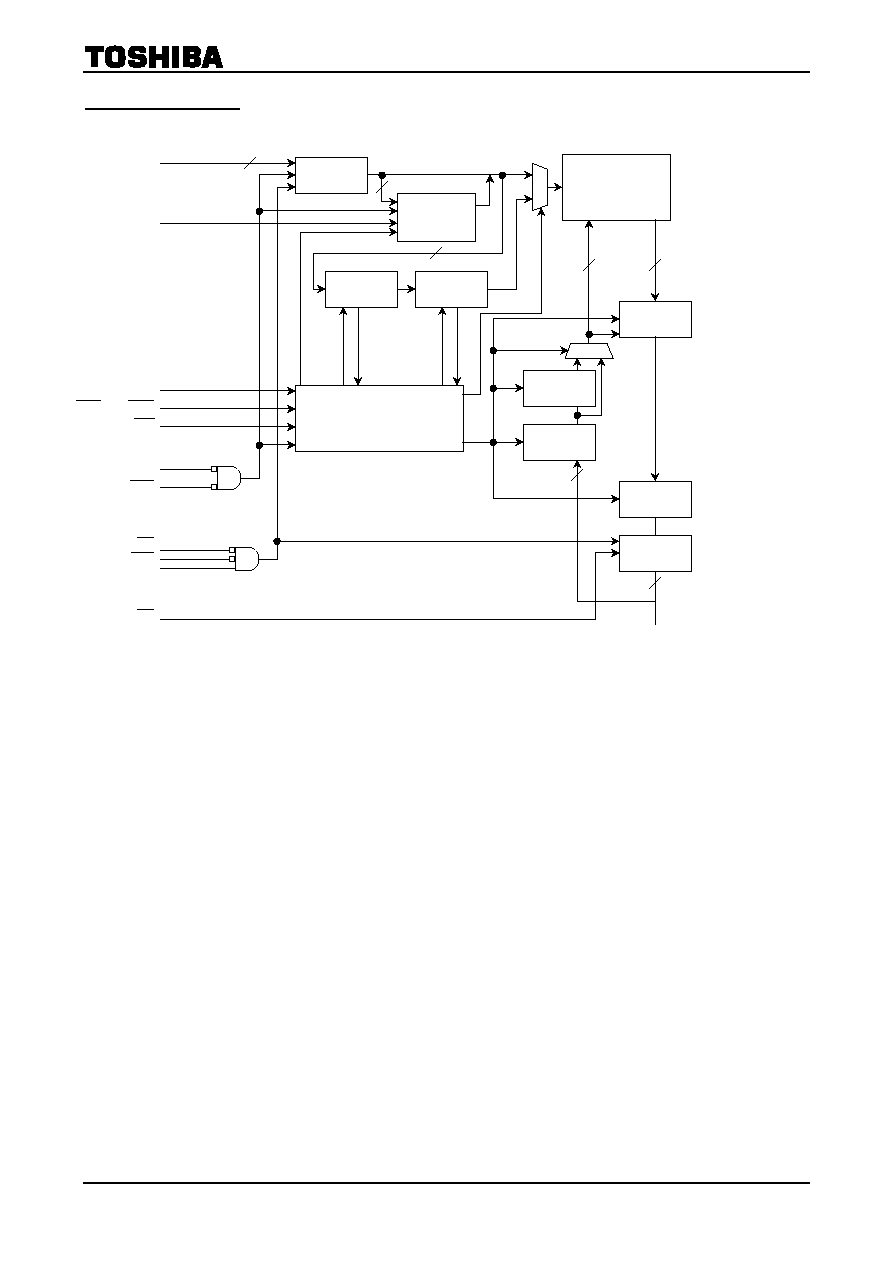
BLOCK DIAGRAM
Binary
Counter and
Logic
A0 /A1
Read/Write Control Logic
&
Coherency Control Logic
Memory
Cell Array
256 K
� 36 bits
(9,437,184 bits)
Address
Register
Address
Register 1
Address
Register 2
Din
Register 2
Din
Register 1
Output
Register
18
18
36
36
36
ADV
BW1
to
BW4
WE
Data-Out
Control
A0 to A17
MODE
Data-Out
Control
36
I/O, I/OP
CLK
CKE
CE2
CE
OE
CE2

TC55VD836FFI-133,-143
2003-02-20 3/21
PIN DESCRIPTIONS
PIN NUMBER
SYMBOL
TYPE
DESCRIPTION
89 CLK
Input
(NA)
Clock Input
All synchronous input signals are registered on the rising edge of
CLK. When the chip is enabled, address inputs and control pins
except for
OE
and ZZ must meet the specified setup and hold
times with respect to the CLK rising edge.
37, 36, 35, 34, 33, 32, 100,
99, 82, 81, 44, 45, 46, 47,
48, 49, 50, 83
A0 to A17
Input
(synchronous)
Address Inputs
These address inputs are registered on the rising edge of CLK.
When the chip is enabled, address inputs must meet the
specified setup and hold times with respect to the CLK rising
edge.
98
CE
Input
(synchronous)
Chip Enable Input
This active-Low signal controls the chip status (enabled or
disabled). It is sampled only when a new external address is
loaded.
92
CE2
Input
(synchronous)
Chip Enable Input
This active-Low signal controls the chip status (enabled or
disabled). It is sampled only when a new external address is
loaded.
97 CE2
Input
(synchronous)
Chip Enable Input
This active-High signal controls the chip status (enabled or
disabled). It is sampled only when a new external address is
loaded.
86
OE
Input
(asynchronous)
Output Enable Input
This active-Low signal controls all 36 bits of the I/O output buffer.
88
WE
Input
(synchronous)
Write Enable Input
This active-Low input controls Read/Write operations.
93, 94, 95, 96
BW1
to
BW4
Input
(synchronous)
Byte Write Enable
These active-Low inputs control Byte Write operations when a
Write cycle is active. A Byte Write pin controls I/O pins as follows.
BW1
: I/O1 to I/O8, I/OP1
BW2
: I/O9 to I/O16, I/OP2
BW3
: I/O17 to I/O24, I/OP3
BW4
: I/O25 to I/O32, I/OP4
85 ADV
Input
(synchronous)
Address Advance Input
This is used to load the internal registers with the input from the
address and control signals when it is Low on the rising edge of
CLK. When it is High, the internal burst address counter is
incremented. The external address inputs are ignored when this
signal is High.
87
CKE
Input
(synchronous)
Clock Enable
When High, CLK input is ignored and outputs retain the same
state.
64 ZZ
Input
(asynchronous)
Snooze Input
This active-High signal is used to place the device into Sleep
Mode (Low-Power Standby Mode). When Low, the device
remains in the Active state. When High, the device goes into the
Sleep state and memory data is retained. After this signal has
been de-asserted, the device will wake up when a read or write
operation is initiated by ADV.

TC55VD836FFI-133,-143
2003-02-20 4/21
PIN NUMBER
SYMBOL
TYPE
DESCRIPTION
52, 53, 56, 57, 58, 59, 62,
63, 68, 69, 72, 73, 74, 75,
78, 79, 2, 3, 6, 7, 8, 9, 12,
13, 18, 19, 22, 23, 24, 25,
28, 29
I/O1 to I/O32
I/O
(synchronous)
Data Input/Output
51, 80, 1, 30
I/OP1 to I/OP4
I/O
(synchronous)
Parity Data Input/Output
31 MODE
Input
(synchronous)
Mode Select Input
This signal selects the burst sequence. When High, the burst
sequence is interleaved. When Low, it is linear.
39, 42, 43, 84
NC
NC
Not Connected
38 NU
Input
(asynchronous)
Not Usable
14, 15, 16, 41, 65, 66, 91
VDD
Supply
Power Supply for Core
4, 11, 20, 27, 54, 61, 70,
77
VDDQ Supply Power Supply for Output Buffers
17, 40, 67, 90
VSS
Ground
Ground for Core
5, 10, 21, 26, 55, 60, 71,
76
VSSQ Ground Ground for Output Buffers
TC55VD836FFI-133,-143
2003-02-20 5/21
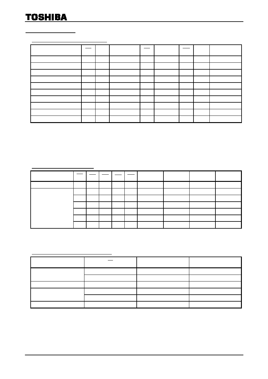
OPERATING MODE
(1) Synchronous Input Truth Table
OPERATION
WE
ADV
CE
BW
Addr. Used
CKE
ZZ
I/O
(2 cycles later)
Read
(begin
burst)
H L
Select
X External L L
Output
Read (continue burst)
X
H
X
X
Internal
L
L
Output
Write (begin burst)
L
L
Select
L
External
L
L
Input
Write (continue burst)
X
H
X
L
Internal
L
L
Input
NOP/Write Abort (begin burst)
L
L
Select
H
X
L
L
Hi-Z
Write Abort (continue burst)
X
H
X
H
Internal
L
L
Hi-Z
Deselected X
L
Deselect
X
X
L
L
Hi-Z
Deselect Continue (Note 2)
X
H
X
X
X
L
L
Hi-Z
Ignore Clock Edge (Note 3)
X
X
X
X
X
H
L
Previous value
Snooze X
X
X
X
X
X
H
Hi-Z
Notes: 1. H means logical High and L means logical Low. X means Don't care.
2. A Deselect Continue cycle can only be entered if a Deselect cycle is executed before it.
3. When the Ignore Clock Edge command is asserted during a Read operation, the output data for the previous cycle still
appear on the I/O pins. When the command is asserted during a Write operation, the I/O pins remain at Hi-Z and the
Write operation is not executed.
4. All synchronous Inputs must exhibit adequate setup and hold times either side of the rising edge of the CLK pin.
5. ZZ input is asynchronous, but is included is this table.
(2) Write Enable Truth Table
OPERATION
WE
BW1
BW2
BW3
BW4
I/O1 to I/O8
I/OP1
I/O9 to I/O16
I/OP2
I/O17 to I/O24
I/OP3
I/O25 to I/O32
I/OP4
Read
H
X
X
X
X
Output Output Output Output
L
L
L
L
L
Input Input Input Input
L L H H H Input
Hi-Z
Hi-Z
Hi-Z
L H L H H
Hi-Z
Input
Hi-Z
Hi-Z
L
H
H
L
H
Hi-Z Hi-Z Input Hi-Z
L H H H L
Hi-Z
Hi-Z
Hi-Z
Input
Write
L
H
H
H
H
Hi-Z Hi-Z Hi-Z Hi-Z
Notes: 1. H means logical High and L means logical Low. X means Don't care.
2. The status for I/O pins described in this column appears two clock cycles after the cycle in which the Read or Write
command is asserted.
(3) Asynchronous Inputs Truth Table
OPERATION
OE
ZZ I/O
L L
Dout
Read
H L
Hi-Z
Write X
L
Din,
Hi-Z
H L
Hi-Z
Stop clock (Note 2)
L L
Low-Z
Snooze (Note 3)
X
H
Hi-Z
Notes: 1. H means logical High and L means logical Low. X means Don't care.
2. The Stop CLK Mode achieves Low-Power Standby by stopping the input clock.
3. The Snooze Mode achieves Low-Power Standby by asserting the ZZ pin.
4. The cycle immediately prior to a Snooze brought about by the ZZ pin must be a Read Mode or Deselect Mode cycle.
5. Memory data is retained during Snooze Mode cycles.