TC55VZM216AJJN/AFTN08,10,12
2003-01-17 1/11
∑ Single power supply voltage of 3.3 V ± 0.3 V
∑ Fully static operation
∑ All inputs and outputs are LVTTL compatible
∑ Output buffer control using OE
∑ Data byte control using LB (I/O1 to I/O8) and
UB (I/O9 to I/O16)
∑ Package:
SOJ44-P-400-1.27 (AJJN)
(Weight: 1.64 g typ)
TSOP II44-P-400-0.80 (AFTN) (Weight: 0.45 g typ)
TOSHIBA MOS DIGITAL INTEGRATED CIRCUIT SILICON GATE CMOS
262,144-WORD BY 16-BIT CMOS STATIC RAM
DESCRIPTION
The TC55VZM216AJJN/AFTN is a 4,194,304-bit high-speed static random access memory (SRAM) organized as
262,144 words by 16 bits. Fabricated using CMOS technology and advanced circuit techniques to provide high
speed, it operates from a single 3.3 V power supply. Chip enable ( CE ) can be used to place the device in a
low-power mode, and output enable ( OE ) provides fast memory access. Data byte control signals ( LB , UB ) provide
lower and upper byte access. This device is well suited to cache memory applications where high-speed access and
high-speed storage are required. All inputs and outputs are directly LVTTL compatible. The
TC55VZM216AJJN/AFTN is available in plastic 44-pin SOJ and TSOP with 400mil width for high density surface
assembly.
FEATURES
∑ Fast access time (the following are maximum values)
TC55VZM216AJJN/AFTN08:8
ns
TC55VZM216AJJN/AFTN10:10 ns
TC55VZM216AJJN/AFTN12:12 ns
∑ Low-power dissipation (I
DDO2
)
(the following are maximum values)
Cycle Time
8
10
12
ns
Operation (max)
140
130
120
mA
Standby:4 mA (both devices)
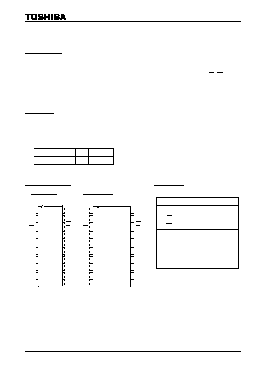
PIN ASSIGNMENT
(TOP VIEW)
PIN NAMES
44 PIN SOJ 44
PIN
TSOP
A0 to A17
Address Inputs
I/O1 to I/O16 Data Inputs/Outputs
CE
Chip
Enable
Input
WE
Write Enable Input
OE
Output Enable Input
LB
,
UB
Data Byte Control Inputs
V
DD
Power
(
+3.3 V)
GND Ground
NU
Not Usable (Input)
A4
A3
A2
A1
A0
I/O1
I/O2
I/O3
I/O4
V
DD
GND
I/O5
I/O6
I/O7
I/O8
A15
A14
A13
A12
A16
A5
A6
A7
I/O16
I/O15
I/O14
I/O13
GND
V
DD
I/O12
I/O11
I/O10
I/O9
NU
A8
A9
A10
A11
A17
1 44
2 43
3 42
4 41
5 40
6 39
7 38
8 37
9 36
10 35
11 34
12 33
13 32
14 31
15 30
16 29
17 28
18 27
19 26
20 25
21 24
22 23
CE
OE
UB
LB
WE
1 44
2 43
3 42
4 41
5 40
6 39
7 38
8 37
9 36
10 35
11 34
12 33
13 32
14 31
15 30
16 29
17 28
18 27
19 26
20 25
21 24
22 23
A4
A3
A2
A1
A0
I/O1
I/O2
I/O3
I/O4
V
DD
GND
I/O5
I/O6
I/O7
I/O8
A15
A14
A13
A12
A16
A5
A6
A7
I/O16
I/O15
I/O14
I/O13
GND
V
DD
I/O12
I/O11
I/O10
I/O9
NU
A8
A9
A10
A11
A17
OE
UB
LB
CE
WE
(TC55VZM216AJJN)
(TC55VZM216AFTN)

TC55VZM216AJJN/AFTN08,10,12
2003-01-17 2/11
BLOCK DIAGRAM
MAXIMUM RATINGS
SYMBOL RATING
VALUE
UNIT
V
DD
Power Supply Voltage
-0.5 to 4.6
V
V
IN
Input Terminal Voltage
-0.5* to 4.6
V
V
I/O
Input/Output Terminal Voltage
-0.5* to V
DD
+ 0.5** V
P
D
Power Dissipation
1.4
W
T
solder
Soldering Temperature (10s)
260
∞C
T
stg
Storage Temperature
-65 to 150
∞C
T
opr
Operating Temperature
-10 to 85
∞C
*:
-1.5 V with a pulse width of 20% of t
RC
min (4 ns max)
**: V
DD
+ 1.5 V with a pulse width of 20% of t
RC
min (4 ns max)
I/O1
CE
V
DD
GND
I/O8
WE
CE
CE
I/O9
OE
UB
LB
CE
A2 A3 A6 A7 A10 A11 A12
A0
A1
A4
A5
A8
A9
A13
A14
A15
A17
A16
CLOCK
GENERATOR
COLUMN ADDRESS BUFFER
COLUMN DECODER
SENSE AMP
MEMORY CELL ARRAY
1,024
◊ 256 ◊ 16
(4,194,304)
I/O2
I/O3
I/O4
I/O5
I/O6
I/O7
I/O10
I/O11
I/O12
I/O13
I/O14
I/O15
I/O16
DA
T
A
OUTP
UT
BU
FFER
DA
T
A
IN
PU
T
BU
FFER
DA
T
A
IN
PU
T
BU
FFER
DA
T
A
OUTP
UT
BU
FFER
RO
W
A
DDRE
SS
BU
F
F
ER
RO
W
DE
CODE
R

TC55VZM216AJJN/AFTN08,10,12
2003-01-17 3/11
DC RECOMMENDED OPERATING CONDITIONS
(Ta
=
=
=
= 0∞ to 70∞C)
SYMBOL PARAMETER MIN TYP MAX UNIT
V
DD
Power Supply Voltage
3.0
3.3
3.6
V
V
IH
Input High Voltage
2.0
V
DD
+ 0.3** V
V
IL
Input Low Voltage
-0.3*
0.8 V
*:
-1.0 V with a pulse width of 20% of t
RC
min (4 ns max)
**: V
DD
+ 1.0 V with a pulse width of 20% of t
RC
min (4 ns max)
DC CHARACTERISTICS
(Ta
=
=
=
= 0∞ to 70∞C, V
DD
=
=
=
= 3.3 V ±±±± 0.3 V)
SYMBOL PARAMETER
TEST
CONDITION
MIN
TYP
MAX
UNIT
I
IL
Input Leakage Current
(Except NU pin)
V
IN
= 0 to V
DD
-1
1 µA
I
LO
Output Leakage
Current
CE
= V
IH
or WE
= V
IL
or
OE
= V
IH
,
V
OUT
= 0 to V
DD
-1
1 µA
I
I (NU)
Input Leakage Current
(NU pin)
V
IN
= 0 V
-1
1 µA
I
OH
= -2 mA
2.4
V
OH
Output High Voltage
I
OH
= -100 µA V
DD
- 0.2
I
OL
= 2 mA
0.4
V
OL
Output Low Voltage
I
OL
= 100 µA
0.2
V
t
cycle
= 8 ns
170
t
cycle
= 10 ns
160
I
DDO1
CE
= V
IL
, I
OUT
= 0 mA,
OE
= V
IH
,
Other Input
= V
IH
/V
IL
t
cycle
= 12 ns
150
t
cycle
= 8 ns
140
t
cycle
= 10 ns
130
I
DDO2
Operating Current
CE
= 0.2 V, I
OUT
= 0 mA,
OE
= V
DD
- 0.2 V,
Other Input
= V
DD
- 0.2 V/0.2 V
t
cycle
= 12 ns
120
mA
I
DDS1
CE
= V
IH
, Other Input
= V
IH
or V
IL
55
I
DDS2
Standby Current
CE
= V
DD
- 0.2 V, Other Input = V
DD
- 0.2 V or 0.2 V
4
mA
CAPACITANCE
(Ta
=
=
=
= 25∞C, f ==== 1 .0 MHz)
SYMBOL PARAMETER
TEST
CONDITION
MAX
UNIT
C
IN
Input
Capacitance
V
IN
= GND
6
pF
C
I/O
Input/Output
Capacitance
V
I/O
= GND
8
pF
Note: This parameter is periodically sampled and is not 100% tested.

TC55VZM216AJJN/AFTN08,10,12
2003-01-17 4/11
OPERATING MODE
MODE
CE
OE
WE
LB
UB
I/O1 to I/O8
I/O9 to I/O16
POWER
L L
Output
Output
I
DDO
H L
High
Impedance
Output
I
DDO
Read L
L
H
L H
Output
High
Impedance I
DDO
L L
Input
Input
I
DDO
H L
High
Impedance
Input
I
DDO
Write L
*
L
L H
Input
High
Impedance I
DDO
L H H * *
Outputs Disable
L
* * H H
High Impedance
High Impedance
I
DDO
Standby H
* * * *
High Impedance
High Impedance
I
DDS
* : Don't care
Note: The NU pin must be left unconnected or tied to GND.
You must not apply a voltage of more than 0.8 V to the NU.

TC55VZM216AJJN/AFTN08,10,12
2003-01-17 5/11
AC CHARACTERISTICS
(Ta
=
=
=
= 0∞ to 70∞C
(See Note 1)
, V
DD
=
=
=
= 3.3 V ±±±± 0.3 V)
READ CYCLE
TC55VZM216AJJN/AFTN
08 10 12
SYMBOL PARAMETER
MIN MAX MIN MAX MIN MAX
UNIT
t
RC
Read
Cycle
Time
8
10 12
t
ACC
Address
Access
Time
8 10 12
t
CO
Chip Enable Access Time
8 10 12
t
OE
Output Enable Access Time
4 5 6
t
BA
Upper Byte, Lower Byte Access Time
4 5 6
t
OH
Output Data Hold Time from Address Change
3
3 3
t
COE
Output Enable Time from Chip Enable
3
3 3
t
OEE
Output Enable Time from Output Enable
0
0 0
t
BE
Output Enable Time from Upper Byte, Lower Byte
0
0 0
t
COD
Output Disable Time from Chip Enable
4 5 6
t
ODO
Output Disable Time from Output Enable
4 5 6
t
BD
Output Disable Time from Upper Byte, Lower Byte
4 5 6
ns
WRITE CYCLE
TC55VZM216AJJN/AFTN
08 10 12
SYMBOL PARAMETER
MIN MAX MIN MAX MIN MAX
UNIT
t
WC
Write
Cycle
Time
8
10 12
t
WP
Write
Pulse
Width
6
7 8
t
CW
Chip Enable to End of Write
6
7 8
t
BW
Upper Byte, Lower Byte Enable to End of Write
6
7 8
t
AW
Address Valid to End of Write
6
7 8
t
AS
Address
Setup
Time
0
0 0
t
WR
Write Recovery Time
0
0 0
t
DS
Data
Setup
Time
4
5 6
t
DH
Data
Hold
Time
0
0 0
t
OEW
Output Enable Time from Write Enable
3
3 3
t
ODW
Output Disable Time from Write Enable
4 5 6
ns
AC TEST CONDITIONS Fig.1
PARAMETER TEST
CONDITION
Input Pulse Level
3.0 V/ 0.0 V
Input Pulse Rise and Fall Time
2 ns
Input Timing Measurement
Reference Level
1.5 V
Output Timing Measurement
Reference Level
1.5 V
Output Load
Fig.1
I/O pin
C
L
= 30 pF
Z
0
= 50
R
L
= 50
V
L
= 1.5 V
I/O pin
C
L
= 5 pF
870
(For t
COE
, t
OEE
, t
BE
, t
COD
,
t
BD
, t
ODO
, t
OEW
and t
ODW
)
3.3 V
1200