
TC58FVT641/B641FT/XB-70,-10
2002-10-24 1/53
∑ Block erase architecture
8 ◊ 8 Kbytes / 127 ◊ 64 Kbytes
∑ Boot block architecture
TC58FVT641FT/XB: top boot block
TC58FVB641FT/XB: bottom boot block
∑ Mode control
Compatible with JEDEC standard commands
∑ Erase/Program cycles
10
5
cycles typ.
∑ Access time
70 ns (C
L
: 30 pF)
100 ns (C
L
: 100 pF)
∑ Power consumption
10 µA (Standby)
30 mA (Read operation)
15 mA (Program/Erase operations)
∑ Package
TC58FVT641/B641FT:
TSOPI48-P-1220-0.50 (weight: 0.52 g)
TC58FVT641/B641XB:
P-TFBGA63-0911-0.80AZ (Weight: 0.170 g)
TOSHIBA MOS DIGITAL INTEGRATED CIRCUIT SILICON GATE CMOS
64-MBIT (8M
◊ 8 BITS / 4M ◊ 16 BITS) CMOS FLASH MEMORY
DESCRIPTION
The TC58FVT641/B641 is a 67,108,864-bit, 3.0-V read-only electrically erasable and programmable flash memory
organized as 8,388,608 words ◊ 8 bits or as 4,194,304 words ◊ 16 bits. The TC58FVT641/B641 features commands
for Read, Program and Erase operations to allow easy interfacing with microprocessors. The commands are based
on the JEDEC standard. The Program and Erase operations are automatically executed in the chip. The
TC58FVT641/B641 also features a Simultaneous Read/Write operation so that data can be read during a Write or
Erase operation.
FEATURES
∑ Power supply voltage
V
DD
= 2.7 V~3.6 V
∑ Operating temperature
Ta = -40∞C~85∞C
∑ Organization
8M ◊ 8 bits / 4M ◊ 16 bits
∑ Functions
Simultaneous Read/Write
Auto Program, Auto Erase
Fast Program Mode / Acceleration Mode
Program Suspend/Resume
Erase Suspend/Resume
data polling / Toggle bit
block protection, boot block protection
Automatic Sleep, support for hidden ROM area
common flash memory interface (CFI)
Byte/Word Modes
∑ TOSHIBA is continually working to improve the quality and reliability of its products. Nevertheless, semiconductor devices in general
can malfunction or fail due to their inherent electrical sensitivity and vulnerability to physical stress. It is the responsibility of the
buyer, when utilizing TOSHIBA products, to comply with the standards of safety in making a safe design for the entire system, and
to avoid situations in which a malfunction or failure of such TOSHIBA products could cause loss of human life, bodily injury or
damage to property.
In developing your designs, please ensure that TOSHIBA products are used within specified operating ranges as set forth in the
most recent TOSHIBA products specifications. Also, please keep in mind the precautions and conditions set forth in the "Handling
Guide for Semiconductor Devices," or "TOSHIBA Semiconductor Reliability Handbook" etc..
∑ The TOSHIBA products listed in this document are intended for usage in general electronics applications (computer, personal
equipment, office equipment, measuring equipment, industrial robotics, domestic appliances, etc.). These TOSHIBA products are
neither intended nor warranted for usage in equipment that requires extraordinarily high quality and/or reliability or a malfunction or
failure of which may cause loss of human life or bodily injury ("Unintended Usage"). Unintended Usage include atomic energy
control instruments, airplane or spaceship instruments, transportation instruments, traffic signal instruments, combustion control
instruments, medical instruments, all types of safety devices, etc.. Unintended Usage of TOSHIBA products listed in this document
shall be made at the customer's own risk.
∑ The products described in this document are subject to the foreign exchange and foreign trade laws.
∑ The information contained herein is presented only as a guide for the applications of our products. No responsibility is assumed by
TOSHIBA CORPORATION for any infringements of intellectual property or other rights of the third parties which may result from its
use. No license is granted by implication or otherwise under any intellectual property or other rights of TOSHIBA CORPORATION or
others.
∑ The information contained herein is subject to change without notice.
000707EBA1
TC58FVT641/B641FT/XB-70,-10
2002-10-24 4/53
MODE SELECTION
BYTE
MODE
WORD
MODE
MODE
CE
OE
WE A9 A6 A1 A0
RESET
/ACC
WP
DQ0~DQ7
(1)
DQ0~DQ15
Read L
L
H
A9
A6
A1
A0
H
*
D
OUT
D
OUT
ID Read (Manufacturer Code)
L L H
V
ID
L L L
H
* Code Code
ID Read (Device Code)
L L H
V
ID
L L H
H
* Code Code
Standby
H
*
*
*
*
*
* H
* High-Z
High-Z
Output Disable
*
H H *
*
*
*
*
* High-Z
High-Z
Write L
H
(2)
A9 A6 A1 A0
H
*
D
IN
D
IN
Block Protect 1
L
V
ID
(2)
V
ID
L H L
H
*
*
*
Verify Block Protect
L
L
H
V
ID
L H L
H
* Code Code
Temporary Block Unprotect
*
*
*
*
*
*
*
V
ID
*
*
*
Hardware Reset / Standby
*
*
*
*
*
*
* L
* High-Z
High-Z
Boot Block Protect
*
*
*
*
*
*
*
* L
*
*
Notes: *
= V
IH
or V
IL
, L
= V
IL
, H
= V
IH
(1) DQ8~DQ14 are High-Z and DQ15/A-1 is Address Input in Byte Mode.
Addresses are A21~A0 in Word Mode ( BYTE
= V
IH
), A21~A-1 in Byte Mode ( BYTE
= V
IL
).
(2) Pulse input
ID CODE TABLE
CODE TYPE
A21~A12
A6
A1
A0
CODE (HEX)
(1)
Manufacturer Code
* L L L
0098H
TC58FVT641
* L L H
0093H
Device Code
TC58FVB641
* L L H
0095H
Verify Block Protect
BA
(2)
L H L Data
(3)
Notes: *
= V
IH
or V
IL
, L
= V
IL
, H
= V
IH
(1) DQ8~DQ14 are High-Z and DQ15/A-1 is Address Input in Byte Mode.
(2) BA: Block Address
(3) 0001H - Protected Block
0000H - Unprotected Block

TC58FVT641/B641FT/XB-70,-10
2002-10-24 5/53
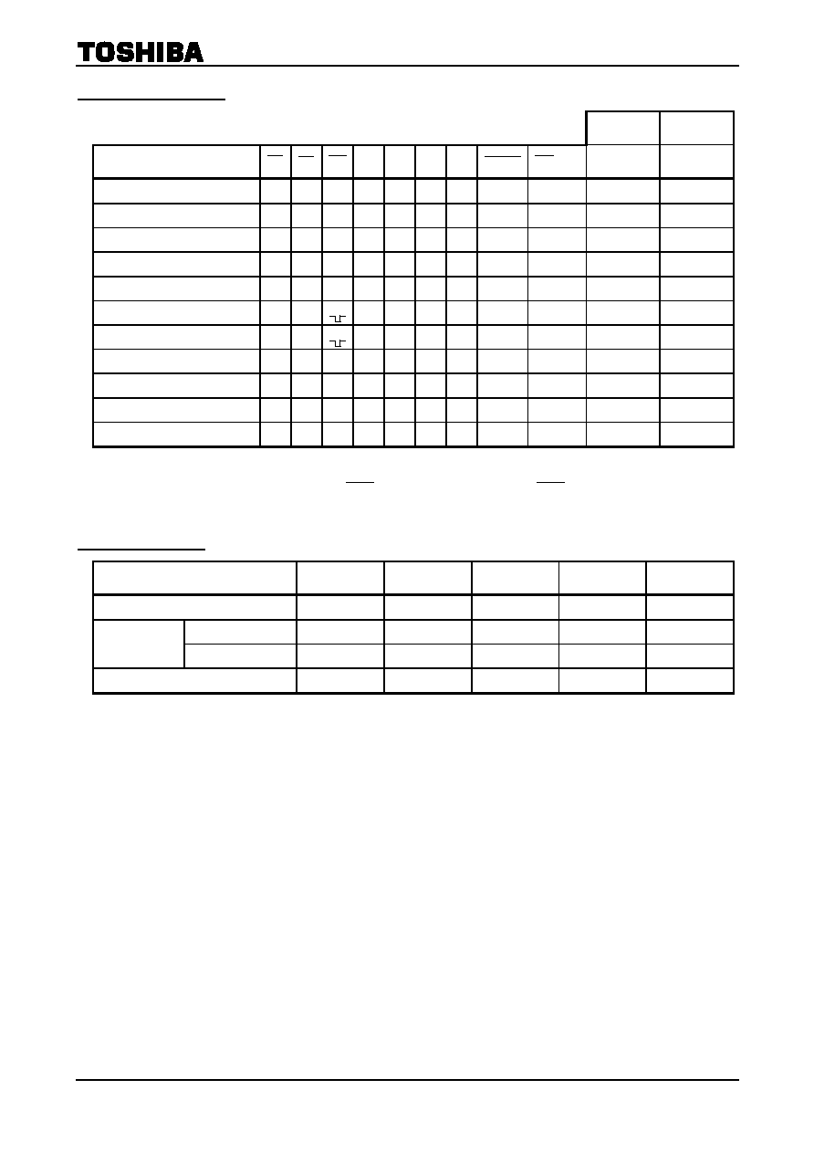
COMMAND SEQUENCES
FIRST BUS
WRITE CYCLE
SECOND BUS
WRITE CYCLE
THIRD BUS
WRITE CYCLE
FOURTH BUS
WRITE CYCLE
FIFTH BUS
WRITE CYCLE
SIXTH BUS
WRITE CYCLE
COMMAND
SEQUENCE
BUS
WRITE
CYCLES
REQ'D
Addr. Data Addr. Data Addr. Data Addr. Data Addr. Data Addr. Data
Read/Reset 1
XXXH
F0H
Word 555H
2AAH 555H
Read/Reset
Byte
3
AAAH
AAH
555H
55H
AAAH
F0H RA
(1)
RD
(2)
Word 555H
2AAH
BK
(3)
+
555H
ID Read
Byte
3
AAAH
AAH
555H
55H
BK
(3)
+
AAAH
90H IA
(4)
ID
(5)
Word 555H
2AAH 555H
Auto-Program
Byte
4
AAAH
AAH
555H
55H
AAAH
A0H PA
(6)
PD
(7)
Program Suspend
1
BK
(3)
B0H
Program Resume
1
BK
(3)
30H
Word 555H
2AAH 555H
555H 2AAH
555H
Auto Chip
Erase
Byte
6
AAAH
AAH
555H
55H
AAAH
80H
AAAH
AAH
555H
55H
AAAH
10H
Word 555H
2AAH 555H
555H 2AAH
Auto Block
Erase
Byte
6
AAAH
AAH
555H
55H
AAAH
80H
AAAH
AAH
555H
55H BA
(8)
30H
Block Erase Suspend
1
BK
(3)
B0H
Block Erase Resume
1
BK
(3)
30H
Block Protect 2
4
XXXH
60H
BPA
(9)
60H XXXH
40H
BPA
(9)
BPD
(10)
Word 555H
2AAH
BK
(3)
+
555H
Verify Block
Protect
Byte
3
AAAH
AAH
555H
55H
BK
(3)
+
AAAH
90H BPA
(9)
BPD
(10)
Word 555H
2AAH 555H
Fast Program
Set
Byte
3
AAAH
AAH
555H
55H
AAAH
20H
Fast Program
2
XXXH
A0H
PA
(6)
PD
(7)
Fast Program Reset
2
XXXH
90H
XXXH
F0H
(13)
Word 555H
2AAH 555H
Hidden ROM
Mode Entry
Byte
3
AAAH
AAH
555H
55H
AAAH
88H
Word 555H
2AAH 555H
Hidden ROM
Program
Byte
4
AAAH
AAH
555H
55H
AAAH
A0H PA
(6)
PD
(7)
Word 555H
2AAH 555H
555H 2AAH
Hidden ROM
Erase
Byte
6
AAAH
AAH
555H
55H
AAAH
80H
AAAH
AAH
555H
55H BA
(8)
30H
Word 555H
2AAH 555H
Hidden ROM
Mode Exit
Byte
4
AAAH
AAH
555H
55H
AAAH
90H XXXH 00H
Word
BK
(3)
+
55H
Query
Command
Byte
2
BK
(3)
+
AAH
98H CA
(11)
CD
(12)
Notes: The system should generate the following address patterns:
Word Mode: 555H or 2AAH on address pins A10~A0
Byte Mode: AAAH or 555H on address pins A10~A-1
DQ8~DQ15 are ignored in Word Mode.
(1) RA: Read
Address
(2) RD: Read
Data
(3) BK: Bank
Address
= A21~A15
(4) IA: Bank Address and ID Read Address (A6, A1, A0)
Bank Address
= A21~A15
Manufacturer Code
= (0, 0, 0)
Device Code
= (0, 0, 1)
(5) ID: ID
Data
(6) PA: Program
Address
(7) PD: Program Data
(8) BA: Block Address
= A21~A12
(9) BPA: Block Address and ID Read Address (A6, A1, A0)
Block Address
= A21~A12
ID Read Address
= (0, 1, 0)
(10) BPD:
Verify Data
(11) CA: CFI Address
(12) CD: CFI Data
(13) F0H: 00H is valid too

