
TC58FVM7(T/B)2AFT(65/80)
2002-10-24 1/68
∑
Access Time (Random/Page)
TC58FVM7T2A/B2AFT65
TC58FVM7T2A/B2AFT80
V
DD
CL
=
30 pF CL
=
100 pF CL
=
30 pF CL
=
100 pF
2.7~3.6V 65 ns/25 ns 70 ns/30 ns 80 ns/30 ns 85 ns/35 ns
2.3~3.6V 70 ns/30 ns 75 ns/35 ns 85 ns/35 ns 90 ns/40 ns
∑
Power consumption
10
µ
A (Standby)
15 mA (Program/Erase operation)
55 mA (Random Read operation)
11 mA (Address Increment Read operation)
5 mA (Page Read operation)
∑
Package
TSOP56-P-1420-0.50A (weight: 0.61g)
TOSHIBA MOS DIGITAL INTEGRATED CIRCUIT SILICON GATE CMOS
128-MBIT (16M
◊
8 BITS / 8M
◊
16 BITS) CMOS FLASH MEMORY
DESCRIPTION
The TC58FVM7T2A/B2A is a 134217728-bit, 3.0-V read-only electrically erasable and programmable flash
memory organized as 16777216 words
◊
8 bits or as 8388608 words
◊
16 bits. The TC58FVM7T2A/B2A features
commands for Read, Program and Erase operations to allow easy interfacing with microprocessors. The commands
are based on the JEDEC standard. The Program and Erase operations are automatically executed in the chip. The
TC58FVM7T2A/B2A also features a Simultaneous Read/Write operation so that data can be read during a Write or
Erase operation.
FEATURES
∑
Power supply voltage
V
DD
=
2.3 V~3.6 V
∑
Operating temperature
Ta
=
-
40
∞
C~85
∞
C
∑
Organization
16M
◊
8 bits/8M
◊
16 bits
∑
Functions
∑
Simultaneous Read/Write
Page Read
Auto Program, Auto Page Program
Auto Block Erase, Auto Chip Erase
Fast Program Mode / Acceleration Mode
Program Suspend/Resume
Erase Suspend/Resume
data polling/Toggle bit
block protection, boot block protection
Automatic Sleep, support for hidden ROM area
common flash memory interface (CFI)
Byte/Word Modes
∑
Block erase architecture
8
◊
8 Kbytes/255
◊
64 Kbytes
∑
Boot block architecture
TC58FVM7T2A: top boot block
TC58FVM7B2A: bottom boot block
∑
Mode control
Compatible with JEDEC standard commands
∑
Erase/Program cycles
10
5
cycles typ.
TC58FVM7(T/B)2AFT(65/80)
2002-10-24 2/68
Ordering information
TC58 F V M7 T2 A FT 65
Speed
version
65
=
65 ns, 80
=
80 ns
Package
FT
=
TSOP
Design
rule
A
=
0.16
µ
m
Function/Boot block architecture/Bank ratio
T2
=
Page mode/Top boot block/1:3:3:1
B2
=
Page mode/Bottom boot block/1:3:3:1
Capacity
M7
=
128Mbits
Supply
Voltage
V
=
3V system
Device
type
F
=
NOR Flash memory
Toshiba CMOS E
2
PROM
Ordering type
Boot block
Speed version
Package
TC58FVM7T2AFT65 Top
TC58FVM7B2AFT65 Bottom
65ns
TC58FVM7T2AFT80 Top
TC58FVM7B2AFT80 Bottom
85ns
TSOP
I56
-P-1420-0.50

TC58FVM7(T/B)2AFT(65/80)
2002-10-24 3/68
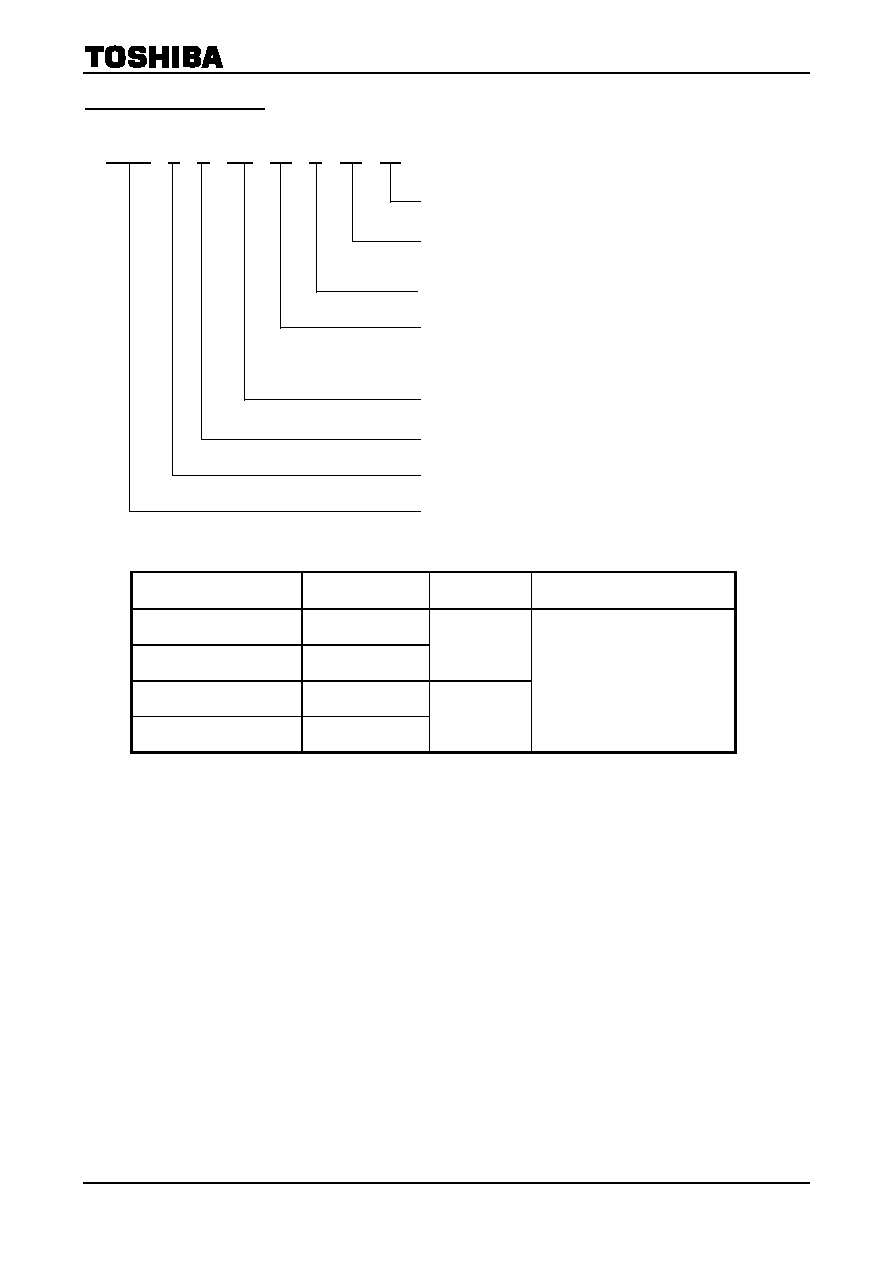
PIN ASSIGNMENT
(TOP VIEW)
PIN NAMES
A-1, A0~A22 Address Input
DQ0~DQ15 Data
Input/Output
CE
Chip
Enable
Input
OE
Output Enable Input
BYTE Word/Byte
Select
Input
WE
Write Enable Input
BY
/
RY
Ready/Busy
Output
RESET
Hardware
Reset
Input
/ACC
WP
Write Protect /
Program Acceleration Input
V
DD
Power
Supply
V
SS
Ground
1
2
3
4
5
6
7
8
9
10
11
12
13
14
15
16
17
18
19
20
21
22
23
24
25
26
27
28
56
55
54
53
52
51
50
49
48
47
46
45
44
43
42
41
40
39
38
37
36
35
34
33
32
31
30
29
N.C
A22
A15
A14
A13
A12
A11
A10
A9
A8
A19
A20
A21
A18
A17
A7
A6
A5
A4
A3
A2
A1
N.C
N.C
WE
RESET
ACC
/
WP
BY
/
RY
N.C
N.C
A16
V
SS
DQ15/A-1
DQ7
DQ14
DQ6
DQ13
DQ5
DQ12
DQ4
V
DD
DQ11
DQ3
DQ10
DQ2
DQ9
DQ1
DQ8
DQ0
V
SS
A0
N.C
N.C
BYTE
OE
CE

TC58FVM7(T/B)2AFT(65/80)
2002-10-24 5/68
MODE SELECTION
BYTE
MODE
WORD
MODE
MODE
CE
OE
WE A9 A6 A1 A0
RESET
/ACC
WP
DQ0~DQ7
(1)
DQ0~DQ15
Read / Page Read
L
L
H
A9
A6
A1
A0
H
*
D
OUT
D
OUT
ID Read (Manufacturer Code)
L L H
V
ID
L L L
H
*
Code Code
ID Read (Device Code)
L L H
V
ID
L L H
H
*
Code Code
Standby
H
*
*
*
*
*
*
H
*
High-Z High-Z
Output Disable
*
H H
*
*
*
*
*
*
High-Z High-Z
Write L
H
(2)
A9 A6 A1 A0 H
*
D
IN
D
IN
Block Protect 1
L
V
ID
(2)
V
ID
L H L
H
*
*
*
Verify Block Protect
L
L
H
V
ID
L H L
H
*
Code Code
Temporary Block Unprotect
*
*
*
*
*
*
*
V
ID
*
*
*
Hardware Reset / Standby
*
*
*
*
*
*
*
L
*
High-Z High-Z
Boot Block Protect
*
*
*
*
*
*
*
*
L
*
*
Notes:
*
=
V
IH
or V
IL
, L
=
V
IL
, H
=
V
IH
(1) DQ8~DQ14 are High-Z and DQ15/A-1 is Address Input in Byte Mode.
Addresses are A22~A0 in Word Mode ( BYTE
=
V
IH
), A22~A-1 in Byte Mode ( BYTE
=
V
IL
).
(2) Pulse input
ID CODE TABLE
CODE TYPE
A22~A12
A6
A1
A0
CODE (HEX)
(1)
Manufacturer Code
*
L L L
0098h
TC58FVM7T2A
*
L L H
007Ch
Device Code
TC58FVM7B2A
*
L L H
0082h
Verify Block Protect
BA
(2)
L H L Data
(3)
Notes:
*
=
V
IH
or V
IL
, L
=
V
IL
, H
=
V
IH
(1) DQ8~DQ14 are High-Z and DQ15/A-1 is Address Input in Byte Mode.
(2) BA: Block Address
(3) 0001h - Protected Block
0000h - Unprotected Block
