
TC74LCX07F/FN/FT
2002-01-11
1
TOSHIBA CMOS Digital Integrated Circuit Silicon Monolithic
TC74LCX07F,TC74LCX07FN,TC74LCX07FT
Low-Voltage HEX Buffer with 5-V Tolerant Inputs and Outputs (open drain)
The TC74LCX07F/FN/FT is a high-performance CMOS buffer.
Designed for use in 3.3-V systems, it achieves high-speed
operation while maintaining the CMOS low power dissipation.
The TC74LCX07 has high performance MOS N-channel
transistor. (open-drain outputs)
The device is designed for low-voltage (3.3 V) V
CC
applications,
but it could be used to interface to 5-V supply environment for
inputs.
All inputs are equipped with protection circuits against static
discharge.
Features
∑ Low-voltage operation: V
CC
= 2.0 to 3.6 V
∑ High-speed operation: t
pz
= 3.7 ns (max) (V
CC
= 3.0 to 3.6 V)
∑ Output current: I
OL
= 24 mA (min) (V
CC
= 3.0 V)
∑ Latch-up performance: -500 mA
∑ Available in JEDEC SOP, JEITA SOP and TSSOP
∑ Open-drain outputs
∑ Power-down protection provided on all inputs and outputs
∑ Pin and function compatible with the 74 series
(74AC/VHC/HC/F/ALS/LS etc.) 07 type
Note: xxxFN (JEDEC SOP) is not available in
Japan.
TC74LCX07F
TC74LCX07FN
TC74LCX07FT
Weight
SOP14-P-300-1.27: 0.18 g (typ.)
SOL14-P-150-1.27: 0.12 g (typ.)
TSSOP14-P-0044-0.65: 0.06 g (typ.)

TC74LCX07F/FN/FT
2002-01-11
2
Pin Assignment
(top view)
IEC Logic Symbol
Truth Table
Systm Diagram
(per gate)
Inputs Outputs
A Y
L L
H Z
Z: High impedance
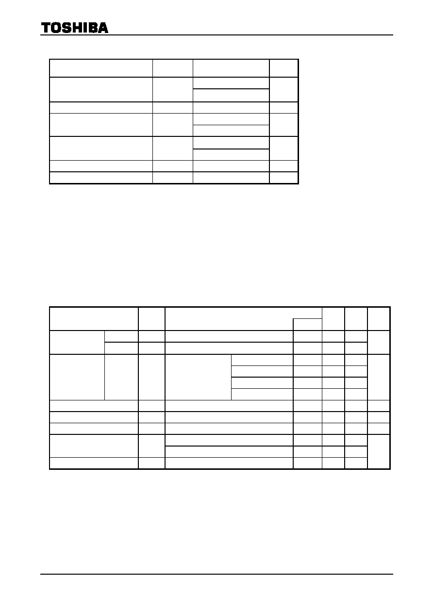
Maximum Ratings
Characteristics Symbol Rating
Unit
Power supply voltage
V
CC
-
0.5 to 7.0
V
DC input voltage
V
IN
-
0.5 to 7.0
V
-
0.5 to 7.0 (Note 1)
DC output voltage
V
OUT
-
0.5 to V
CC
+
0.5
(Note 2)
V
Input diode current
I
IK
-
50 mA
Output diode current
I
OK
-
50 (Note
3)
mA
DC output current
I
OUT
50 mA
Power dissipation
P
D
180 mW
DC V
CC
/ground current
I
CC
/I
GND
±
100 mA
Storage temperature
T
stg
-
65 to 150
∞C
Note 1: Output in OFF state
Note 2: Low state. I
OUT
absolute maximum rating must be observed.
Note 3: V
OUT
<
GND
V
CC
14
6A
6Y
5A
5Y
4A
13
12
11
10
9
8
1A
1
2
3
4
5
6
7
1Y
2A
2Y
3A
3Y
GND
4Y
1A
2A
3A
4A
5A
6A
1Y
2Y
3Y
4Y
5Y
6Y
1
3
5
9
11
13
2
4
6
8
10
12
1
A
Y
TC74LCX07F/FN/FT
2002-01-11
3
Recommended Operating Conditions
Characteristics Symbol Rating
Unit
2.0 to 3.6
Power supply voltage
V
CC
1.5 to 3.6 (Note 4)
V
Input voltage
V
IN
0 to 5.5
V
0 to 5.5 (Note 5)
Output voltage
V
OUT
0
to
V
CC
(Note 6)
V
24
(Note
7)
Output current
I
OL
12
(Note
8)
mA
Operating temperature
T
opr
-
40 to 85
∞C
Input rise and fall time
dt/dv
0 to 10 (Note 9)
ns/V
Note 4: Data retention only
Note 5: Output in OFF state
Note 6: Low state
Note 7: V
CC
=
3.0 to 3.6 V
Note 8: V
CC
=
2.7 to 3.0 V
Note 9: V
IN
=
0.8 to 2.0 V, V
CC
=
3.0 V
Electrical Characteristics
DC Characteristics
(Ta
=
=
=
=
-
-
-
-
40 to 85∞C)
Characteristics Symbol
Test
Condition
V
CC
(V)
Min Max
Unit
H-level V
IH
æ
2.7 to 3.6
2.0
æ
Input voltage
L-level V
IL
æ
2.7 to 3.6
æ
0.8
V
I
OL
=
100
m
A
2.7 to 3.6
æ
0.2
I
OL
=
12 mA
2.7
æ
0.4
I
OL
=
16 mA
3.0
æ
0.4
Output voltage
L-level V
OL
V
IN
=
V
IL
I
OL
=
24 mA
3.0
æ
0.55
V
Input leakage current
I
IN
V
IN
=
0 to 5.5 V
2.7 to 3.6
æ
±
5.0
m
A
Output OFF state current
I
OZ
V
IN
=
V
IH,
V
OUT
=
0 to 5.5 V
2.7 to 3.6
æ
±
5.0
m
A
Power-off leakage current
I
OFF
V
IN
/V
OUT
=
5.5 V
0
æ
10.0
m
A
V
IN
=
V
CC
or GND
2.7 to 3.6
æ
10.0
Quiescent supply current
I
CC
V
IN
/V
OUT
=
3.6 to 5.5 V
2.7 to 3.6
æ
±
10.0
Increase in Icc per input
D
I
CC
V
IH
=
V
CC
-
0.6
2.7 to 3.6
æ
500
m
A

TC74LCX07F/FN/FT
2002-01-11
4
AC Characteristics
(Ta
=
=
=
=
-
-
-
-
40 to 85∞C)
Characteristics Symbol
Test
Condition
V
CC
(V)
Min Max
Unit
2.7 1.0 4.4
Output enable time
t
pZL
Figure 1, Figure 2
3.3
±
0.3
0.8
3.7
ns
2.7 1.0 4.4
Output disable time
t
pLZ
Figure
1,
Figure
2
3.3
±
0.3
0.8
3.7
ns
2.7
æ
æ
Output to output skew
t
osZL
(Note
10)
3.3
±
0.3
æ
1.0
ns
Note 10: Parameter guaranteed by design.
(t
osZL
=
|t
pZLm
-
t
pZLn
|)
Dynamic Switching Characteristics
(Ta
=
=
=
=
25∞C, input: t
r
=
=
=
=
t
f
=
=
=
=
2.5 ns, C
L
=
=
=
=
50 pF, R
L
=
=
=
=
500
W
W
W
W
)
Characteristics Symbol
Test Condition
V
CC
(V)
Typ.
Unit
Quiet output maximum
dynamic V
OL
V
OLP
V
IH
=
3.3 V, V
IL
=
0 V
3.3
0.8
V
Quiet output minimum
dynamic V
OL
|V
OLV
| V
IH
=
3.3 V, V
IL
=
0 V
3.3
0.8
V
Capacitive Characteristics
(Ta
=
=
=
=
25∞C)
Characteristics Symbol
Test Condition
V
CC
(V)
Typ.
Unit
Input capacitance
C
IN
3.3
7
pF
Output capacitance
C
OUT
æ
3.3 8 pF
Power dissipation capacitance
C
PD
f
IN
=
10 MHz
(Note 11)
3.3
5
pF
Note 11: C
PD
is defined as the value of the internal equivalent capacitance which is calculated from the operating
current consumption without load.
Average operating current can be obtained by the equation:
I
CC (opr)
=
C
PD
V
CC
f
IN
+
I
CC
/6 (per gate)
