 | –≠–ª–µ–∫—Ç—Ä–æ–Ω–Ω—ã–π –∫–æ–º–ø–æ–Ω–µ–Ω—Ç: TC9455F | –°–∫–∞—á–∞—Ç—å:  PDF PDF  ZIP ZIP |
TC9455,88F/N
2002-02-05
1
TOSHIBA CMOS Digital Integrated Circuit Silicon Monolithic
TC9455F,TC9455N,TC9488F,TC9488N
Digital Echo IC for Karaoke
The TC9455 series are digital echo ICs for karaoke. The ICs
incorporate microphone amps and volume controllers, enabling a
digital echo system to be configured on a single chip.
Features
∑ Incorporates a two-channel microphone amp with auto level
control (ALC), AD/DA converter, delay memory, and electronic
volume controllers.
∑ Incorporates a 32-kHz sampling, 12-bit successive comparison
AD/DA converter.
∑ Incorporates a delay memory (16-Kbit DRAM) which enables
128-ms (typ.) delay.
∑ Microphone and echo levels are controlled by built-in volume
controllers. They are controlled either by DC voltage or
controlled in serial by the MCU.
TC9455F/N: Supports I
2
C bus interface
TC9488F/N: Supports three-lead interface
∑ The system clock is generated by the CR oscillator circuit.
∑ The echo feedback amount is configured using analog circuits.
The feedback level can be freely set
.
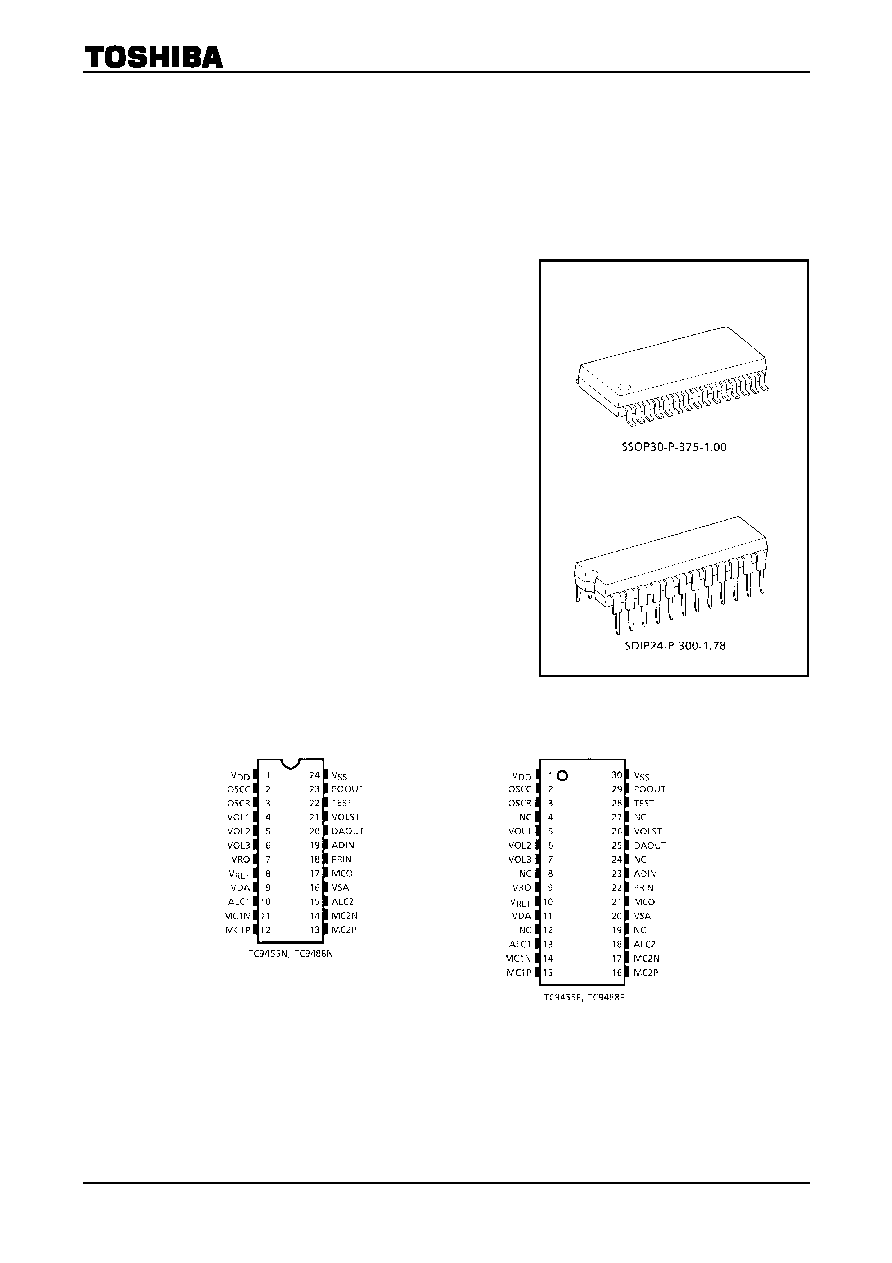
∑ The IC comes in 30-pin flat package or 24-pin shrink DIP.
Pin Connection
TC9455F
TC9488F
TC9455N
TC9488N
Weight:
SSOP30-P-375-1.00: 1.08 g (typ.)
SDIP24-P-300-1.78: 1.2 g (typ.)

TC9455,88F/N
2002-02-05
2
Block Diagram
System Block Diagram

TC9455,88F/N
2002-02-05
3
Pin Description
(Note 1)
Pin Number
TC9455N
TC9488N
TC9455F
TC9488F
Symbol I/O
Function
Remarks
1 1 V
DD
Digital supply voltage pin
2
2
CSCC
I
Capacitor connecting pin for CR oscillator (C = 68 pF)
3
3
OSCR
I
Resistor connecting pin for CR oscillator (R = 5.6 k)
4 5
VOL1
(
CS
) I When VOLST = "H" level,
CS
signal input pin
When VOLST = "L" level, DC control pin for MIC1 volume
5 6
VOL2
(SCL)
I
When VOLST = "H" level, clock input pin
When VOLST = "L" level, DC control pin for MIC2 volume
Open drain output
6 7
VOL3
(SDA)
I
When VOLST = "H" level, data input pin
When VOLST = "L" level, DC control pin for echo volume
Open drain output
7 9 VRO
Reference
voltage
pin
8 10 V
REF
Reference voltage pin (1/2 V
DD
)
9 11 VDA
Analog supply voltage pin
10
13
ALC1
I
Auto level control pin 1
11
14
MC1N
I
MIC1 feedback signal input pin
12
15
MC1P
I
MIC1 signal input pin
13
16
MC2P
I
MIC2 signal input pin
14
17
MC2N
I
MIC2 feedback signal input pin
15
18
ALC2
I
Auto level control pin 2
16 20 VSA
Analog ground pin
17
21
MCO
O MIC addition signal output pin
18
22
PRIN
I
Pre-filter input pin
19
23
ADIN
I
Pre-filter output signal or DC input pin
20
25
DAOUT
O Post-filter output pin
21 26
VOLST
I
Electronic volume control mode select pin
When VOLST = "H" level, serial control (I
2
C bus/three-lead)
When VOLST = "L" level, DC level control
22 28
TEST
I
Test pin. Fix to "H" level for normal use
23
29
POOUT
O Microphone echo signal output pin
24 30 V
SS
Digital ground pin
Note 1: With the TC9455F and TC9488F, pins 4, 8, 12, 19, 24, and 27 are not connected (NC pins).
NC pins are normally open.
TC9455,88F/N
2002-02-05
4
Operation
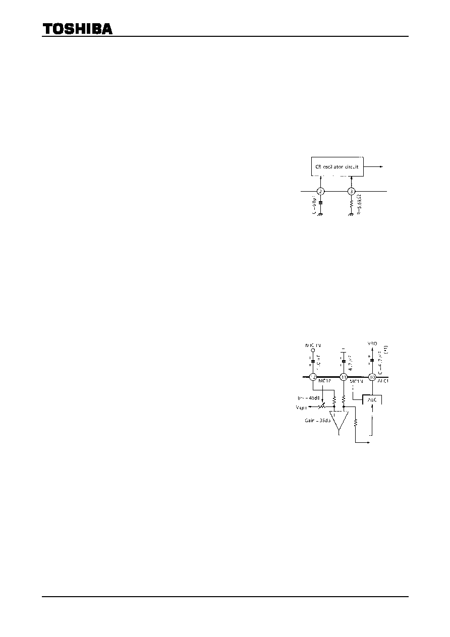
1. Oscillator
circuit
The TC9455F/N and TC9488F/N generate an internal system clock using the CR oscillator circuit.
Connecting a capacitance (C) of 68 pF and a resistance (R) of 5.6 k sets the oscillator frequency to approx.
4 MHz and the sampling frequency to 32 kHz.
Varying the external capacitance enables the oscillator frequency and sampling frequency for the system
clock to be adjusted. Varying the system clock enables the delay time to be adjusted.
Figure 1 shows the CR oscillator circuit.
1.1
How to determine oscillator frequency (f)
f [MHz] = 1532/(C [pF] ◊ R [k])
= 1532/(68 ◊ 5.6)
4.0 MHz (Note 2)
Note 2: The oscillator frequency is a typical value (Ta =
25∞C). Set the resistance to between 4.7 k and
6.8 k.
1.2
How to determine sampling frequency (fs)
fs [kHz] = f/128
=
4.0/128
32 kHz
2. Microphone
amps
The IC incorporates microphone amps with auto level control (ALC).
The microphone amp gain is typically 36dB.
When a signal from 0 to -46dB is input, the ALC circuit can control the output signal level.
Changing the external capacitor connected to the ALC circuit to a resistor sets the ALC circuit to off.
Figure 2 shows the microphone amp circuit.
When C = 4.7 µF, the attack and release times are as follows:
Attack time = Approx. 29 ms
Release time = Approx. 1.6 s
Setting the capacitance (C) to a smaller value enables the
attack and release times to be adjusted. When the ALC circuit
is not used, change the capacitor (*1) to a resistor (approx. 10
k), and connect to GND line.
At power on, while the capacitor is being charged, no sound is
output. So, use a capacitance of 4.7 µF or less.
Figure 1
CR Oscillator circuit
Figure 2
Microphone amp with ALC
TC9455,88F/N
2002-02-05
5
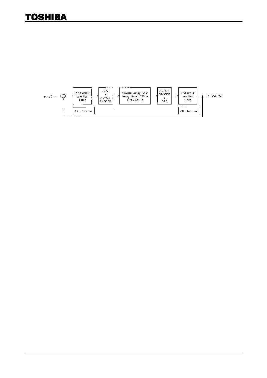
3.
AD/DA converter and digital delay circuit
The AD/DA converter is a 12-bit successive comparison type. The sampling frequency when the system
clock operates at 4 MHz is 32 kHz.
The analog signal input from the AD converter is converted to 12-bit digital data. The digital delay circuit
compresses the 12-bit signal to 4-bit, writes it to delay RAM, then reads it. The 4-bit data read from delay
RAM is de-compressed to 12-bit. The 12-bit data are converted to analog signals by the DA converter and
output.
The area for delay RAM memory is 4096 words ◊ 4 bits.
The echo delay time is 4096 words ◊ (1/32 kHz) = 128 ms.
Figure 3 is a block diagram of the echo circuit.
Figure 3 Block diagram of echo circuit