Dual Output
+Vo
Bipolar
Push-Pull
Inverter
+Vin
-Vin
Com.
-Vo
Positive
Regulator
Negative
Regulator
LC
Filter
Single Output
+Vo
Bipolar
Push-Pull
Inverter
+Vin
-Vin
-Vo
Low
Dropout
Regulator
LC
Filter
Block Diagram
Low Noise
EN55022
EMI
I/O Isolation
4000
VAC
Low Cost
$
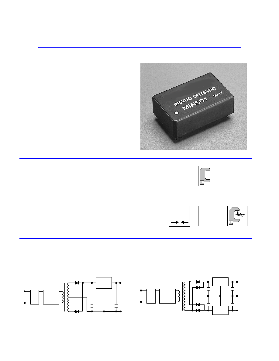
MIR500 2W DC/DC's are specially designed to
provide ultra-high levels of isolation 5600VDC in a
low-profile DIP package.
The series consists of 18 models with input voltages of
5V, 12V and 24V, and offers regulated output voltages of 5V,
12V, 15V in both single and dual output configurations.
The MIR500 series is an excellent selection for a wide
variety of applications including mixed analog/digital
subsystems, railroad/transportation equipments, medical
equipment subsystems, process/machine control equipments
and automatic test instrumentation.
MTBF > 600,000 Hours
EMI Complies With EN55022 Class A
Low Cost
Short Circuit Protection
Regulated Outputs
Low Leakage Current
Low Isolation Capacitance
I/O Isolation 4000VAC
Key Features
Single and Dual Outputs
2 Watts High In/Out Isolation DIP DC/DC Converters
MIR500
Series
TOTAL POWER INT'L

58
142
{66
{15
MIR526
58
143
{83
{12
MIR525
45
93
{100
{5
MIR524
64
130
133
15
MIR523
63
131
165
12
MIR522
62
3
30
134
0
400
5
24
(21.6 ~ 26.4)
MIR521
59
280
{66
{15
MIR516
59
281
{83
{12
MIR515
45
185
{100
{5
MIR514
64
260
133
15
MIR513
63
262
165
12
MIR512
62
8
50
269
0
400
5
12
(10.8 ~ 13.2)
MIR511
57
695
{66
{15
MIR506
57
699
{83
{12
MIR505
42
476
{100
{5
MIR504
64
623
133
15
MIR503
63
629
165
12
MIR502
62
15
100
645
0
400
5
5
(4.5 ~ 5.5)
MIR501
% (Typ.)
mA (Typ.)
mA (Typ.)
mA (Typ.)
mA
mA
VDC
VDC
@Max. Load
@No Load
@Max. Load
Min.
Max.
Efficiency
Reflected
Ripple
Current
Input Current
Output Current
Output
Voltage
Input
Voltage
Model
Number
Model Selection Guide
EN55022 Class A
Conducted EMI
Free-Air Convection
Cooling
%
95
---
Humidity
]
+125
-40
Storage Temperature
]
+90
-25
Case
Operating Temperature
]
+60
-25
Ambient
Operating Temperature
Unit
Max.
Min.
Conditions
Parameter
Environmental Specifications
Exceeding these values can damage the module. These are not continuous
operating ratings.
mW
2,000
---
Internal Power Dissipation
]
260
---
Lead Temperature (1.5mm from case for 10 Sec.)
VDC
30
-0.7
24VDC Input Models
VDC
15
-0.7
12VDC Input Models
VDC
7.5
-0.7
5VDC Input Models
Input Surge Voltage
( 1000 mS )
Unit
Max.
Min.
Parameter
Note :
1. Specifications typical at Ta=+25], resistive
load, nominal input voltage, rated output
current unless otherwise noted.
2. Transient recovery time is measured to within
1% error band for a step change in output load
of 50% to 100%.
3. Ripple & Noise measurement bandwidth is
0-20 MHz.
4. All DC/DC converters should be externally
fused at the front end for protection.
5. Other input and output voltage may be
available, please contact factory.
6. Specifications subject to change without notice.
Absolute Maximum Ratings
MIR500 Series

K Hours
---
---
600
MIL-HDBK-217F @ 25], Ground Benign
MTBF
KHz
80
---
25
Switching Frequency
pF
30
20
---
100KHz,1V
Isolation Capacitance
G[
---
---
10
500VDC
Isolation Resistance
uA
2
---
---
240VAC,60Hz
Leakage Current
VDC
---
---
8000
Flash Tested for 1 Second
Isolation Test Voltage
VDC
---
---
6000
60 Seconds
Isolation Test Voltage
VDC
---
---
5600
Rated Isolation Voltage
Unit
Max.
Typ.
Min.
Conditions
Parameter
General Specifications
Continuous
Output Short Circuit
%/]
{0.02
{0.01
---
Temperature Coefficient
%
{6
---
---
Transient Response Deviation
uS
50
---
---
50% Load Step Change
Transient Recovery Time
%
---
---
120
Over Load
mV rms.
5
---
---
Ripple & Noise (20MHz)
mV P-P
100
---
---
Over Line,Load & Temp
Ripple & Noise (20MHz)
mV P-P
50
30
---
Ripple & Noise (20MHz)
%
{1.0
{0.5
---
Io=10% to 100%
Load Regulation
%
{0.5
{0.3
---
Vin=Min. to Max.
Line Regulation
%
{4.0
{2.0
---
Dual Output Balance Load
Output Voltage Balance
%
{4.0
{2.0
---
Output Voltage Accuracy
Unit
Max.
Typ.
Min.
Conditions
Parameter
Output Specifications
Pi Filter
Input Filter
mW
2000
---
---
Short Circuit Input Power
A
0.5
---
---
All Models
Reverse Polarity Input Current
26.4
24
21.6
24V Input Models
13.2
12
10.8
12V Input Models
VDC
5.5
5
4.5
5V Input Models
Input Voltage Range
Unit
Max.
Typ.
Min.
Model
Parameter
Input Specifications
Note: # For each output .
270
270
270
680
680
680
Maximum Capacitive Load
{15V #
{12V #
{5V #
15V
12V
5V
Models by Vout
Capacitive Load
250mA Slow - Blow Type
500mA Slow - Blow Type
1000mA Slow - Blow Type
24V Input Models
12V Input Models
5V Input Models
Input Fuse Selection Guide
MIR500 Series

Derating Curve
]
Ambient Temperature
Output Power (%)
0
20
40
60
80
100
-40
50
60
80
100
110
90
70
400LFM
200LFM
100LFM
Natural
convection
Efficiency vs Output Load ( Dual Output )
Efficiency vs Output Load ( Single Output )
20
30
40
50
60
70
80
90
Load Current (%)
Efficiency (%)
100
60
40
20
10
80
20
30
40
50
60
70
80
90
Load Current (%)
Efficiency (%)
100
60
40
20
10
80
Efficiency vs Input Voltage ( Dual Output )
Efficiency vs Input Voltage ( Single Output )
30
40
50
60
70
80
Efficiency (%)
Input Voltage (V)
Nom
Low
High
30
40
50
60
70
80
Efficiency (%)
Input Voltage (V)
Nom
Low
High
MIR500 Series

Test Configurations
Input Reflected-Ripple Current Test Setup
Input reflected-ripple current is measured with a inductor
Lin (4.7uH) and Cin (220uF, ESR < 1.0[ at 100 KHz) to
simulate source impedance.
Capacitor Cin, offsets possible battery impedance.
Current ripple is measured at the input terminals of the
module, measurement bandwidth is 0-500 KHz.
Peak-to-Peak Output Noise Measurement Test
Use a Cout 0.33uF ceramic capacitor.
Scope measurement should be made by using a BNC
socket, measurement bandwidth is 0-20 MHz. Position the
load between 50 mm and 75 mm from the DC/DC Converter.
Design & Feature Considerations
Maximum Capacitive Load
The MIR500 series has limitation of maximum connected
capacitance at the output.
The power module may be operated in current limiting
mode during start-up, affecting the ramp-up and the startup
time.
For optimum performance we recommend 220uF
maximum capacitive load
for dual outputs and 470
u
F
capacitive load
for single outputs.
The maximum capacitance can be found in the data.
Input Source Impedance
The power module should be connected to a low
ac-impedance input source. Highly inductive source
impedances can affect the stability of the power module.
In applications where power is supplied over long lines and
output loading is high, it may be necessary to use a capacitor
at the input to ensure startup.
Capacitor mounted close to the power module helps
ensure stability of the unit, it is recommended to use a good
quality low Equivalent Series Resistance (ESR < 1.0[ at 100
KHz) capacitor of a 4.7uF for the 5V input devices and a 2.2uF
for the 12V and 24V devices.
Output Ripple Reduction
A good quality low ESR capacitor placed as close as
practicable across the load will give the best ripple and noise
performance.
To reduce output ripple, it is recommended to use 1.5uF
capacitors at the output.
Thermal Considerations
Many conditions affect the thermal performance of the
power module, such as orientation, airflow over the module
and board spacing. To avoid exceeding the maximum
temperature rating of the components inside the power
module, the case temperature must be kept below 85�C.
The derating curves are determined from measurements
obtained in an experimental apparatus.
MIR500 Series
+Out
-Out
+Vin
-Vin
DC / DC
Converter
Load
Battery
+
Lin
+
Cin
To Oscilloscope
Current
Probe
+Out
-Out
+Vin
-Vin
Dual Output
DC / DC
Converter
Resistive
Load
Scope
Copper Strip
Cout
Com.
Scope
Cout
+Out
-Out
+Vin
-Vin
Single Output
DC / DC
Converter
Resistive
Load
Scope
Copper Strip
Cout
+
+Out
-Out
+Vin
-Vin
DC / DC
Converter
Load
DC Power
Source
+
-
Cin
+Out
-Out
+Vin
-Vin
Load
DC Power
Source
+
-
Cout
Com.
Dual Output
DC / DC
Converter
+Out
-Out
+Vin
-Vin
Load
DC Power
Source
+
-
Cout
Single Output
DC / DC
Converter
DUT
Position of air velocity
probe and thermocouple
50mm / 2in
Air Flow
15mm / 0.6in
Units are encapsulated in a low thermal resistance molding compound which has excellent chemical resistance and electrical
properties in high humidity environment and over a wide operating temperature range.
The encapsulant and outer shell of the unit have UL94V-0 ratings. The leads are tin plated for better soldering.
-Vin
-Vin
24
-Vin
-Vin
23
UL94V-0
:
Flammability
+Vout
No Pin
15
-Vout
+Vout
13
12.4g
:
Weight
No Pin
-Vout
12
Common
No Pin
11
Non-Conductive Black Plastic
:
Case Material
Common
No Pin
10
+Vin
+Vin
2
1.25*0.8*0.4 inches
+Vin
+Vin
1
31.8*20.3*10.2 mm
:
Case Size
Dual Output
Single Output
Pin
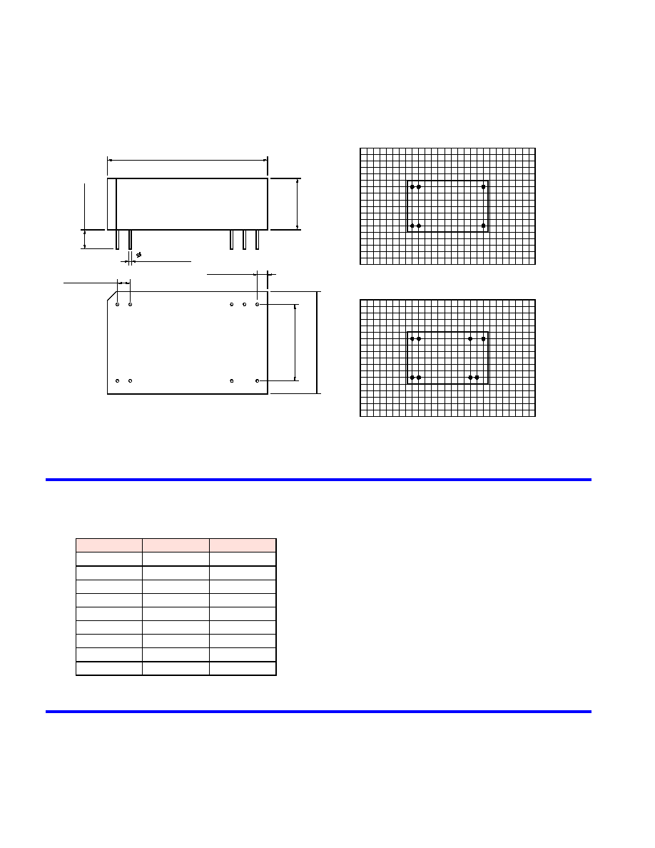
Physical Characteristics
Pin Connections
{0.002
{0.05
Pin
.XXX{0.01
.XX{0.25
.XX{0.01
.X{0.25
Inches
Millimeters
Tolerance
Dual Output
Single Output
31.8 [1.25]
10.2 [0.40
]
20.3 [0.80
]
2.0 [0.08]
Bottom
3.8 [0.15
]
Side
1 2
10 11 12
15
13
24 23
0.50 [0.020]
2.54 [0.100]
15.22 [0
.600]
Connecting Pin Patterns
Top View ( 2.54 mm / 0.1 inch grids )
Mechanical Data
MIR500 Series