February 11, 2003
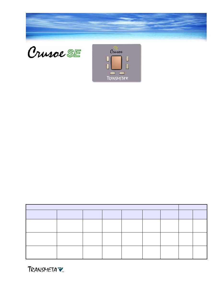
CrusoeTM SE
TM55E/TM58E
Version 2.1
Data Book
Crusoe SE Embedded Processors Described in this Document
Processor
Memory
SKU
Package
Marking
L2 Cache
Max Core
Frequency
Core
Voltage
Temp
Range
TDP
DDR
SDR
TM58EX-933
100�C
DDR/SDR
58EXAE093321 512 KBytes 933 MHz
0.80-1.30 V
0 - 100 �C 9.0 W
Yes
Yes
TM58EL-800
100�C
DDR/SDR
58ELAD080021 512 KBytes 800 MHz
0.80-1.20 V
0 - 100 �C 6.8 W
Yes
Yes
TM55EL-667
100�C
DDR/SDR
55ELAC066721 256 KBytes 667 MHz
0.80-1.10 V
0 - 100 �C 5.1 W
Yes
Yes

Property of:
Transmeta Corporation
3990 Freedom Circle
Santa Clara, CA 95054
USA
(408) 919-3000
http://www.transmeta.com
The information contained in this document is provided solely for use in connection with Transmeta products, and Transmeta
reserves all rights in and to such information and the products discussed herein. This document should not be construed as
transferring or granting a license to any intellectual property rights, whether express, implied, arising through estoppel or
otherwise. Except as may be agreed in writing by Transmeta, all Transmeta products are provided "as is" and without a
warranty of any kind, and Transmeta hereby disclaims all warranties, express or implied, relating to Transmeta's products,
including, but not limited to, the implied warranties of merchantability, fitness for a particular purpose and non-infringement of
third party intellectual property. Transmeta products may contain design defects or errors which may cause the products to
deviate from published specifications, and Transmeta documents may contain inaccurate information. Transmeta makes no
representations or warranties with respect to the accuracy or completeness of the information contained in this document, and
Transmeta reserves the right to change product descriptions and product specifications at any time, without notice.
Transmeta products have not been designed, tested, or manufactured for use in any application where failure, malfunction, or
inaccuracy carries a risk of death, bodily injury, or damage to tangible property, including, but not limited to, use in factory
control systems, medical devices or facilities, nuclear facilities, aircraft, watercraft or automobile navigation or communication,
emergency systems, or other applications with a similar degree of potential hazard.
Transmeta reserves the right to discontinue any product or product document at any time without notice, or to change any
feature or function of any Transmeta product or product document at any time without notice.
Trademarks: Transmeta, the Transmeta logo, Crusoe, the Crusoe logo, Code Morphing, LongRun, and combinations thereof
are trademarks of Transmeta Corporation in the USA and other countries. Other product names and brands used in this
document are for identification purposes only, and are the property of their respective owners.
Copyright � 2001-2003 Transmeta Corporation. All rights reserved.
February 11, 2003
2
CrusoeTM SE TM55E/TM58E Version 2.1
Data Book
CrusoeTM SE Model TM55E/TM58E Version 2.1 Embedded Processor
Data Book
Revision 1.00
Revision History:
1.00
February 11, 2003 - first release of version 2.1embedded data book

February 11, 2003
3
Table of Contents
List of Tables .......................................................................................................................................... 5
List of Figures ......................................................................................................................................... 7
Introduction
............................................................................................................................................. 9
Chapter 1
Functional Interface Description ......................................................................................................... 13
1.1
Power and Thermal Management............................................................................................. 13
1.1.1
Power Management States ........................................................................................ 13
1.1.2
LongRun Power Management .................................................................................... 16
1.1.3
LongRun Thermal Management ................................................................................. 18
1.1.4
Processor Thermal Monitoring.................................................................................... 18
1.1.5
SDRAM Power Saving Modes.................................................................................... 18
1.2
Memory Interfaces .................................................................................................................... 19
1.2.1
DDR SDRAM Interface ............................................................................................... 19
1.2.2
DDR Memory Interface Constraints............................................................................ 20
1.2.3
DDR Interface Reference Voltage Circuit ................................................................... 20
1.2.4
SDR SDRAM Interface ............................................................................................... 21
1.2.5
SDR Memory Interface Constraints ............................................................................ 22
1.3
System Memory Configurations ................................................................................................ 23
1.3.1
Recommended Memory Configurations ..................................................................... 23
1.3.2
Code Morphing Software Memory .............................................................................. 25
1.4
PCI Interface ............................................................................................................................. 26
1.4.1
PCI Bus Commands ................................................................................................... 26
1.4.2
Bus Arbitration ............................................................................................................ 27
1.5
Southbridge Sideband Signals.................................................................................................. 28
1.6
Serial Interfaces ........................................................................................................................ 28
1.7
Clocks ....................................................................................................................................... 29
1.8
JTAG Test Interface .................................................................................................................. 29
1.9
Supply Voltages ........................................................................................................................ 29
1.10
Core Voltage Regulator VRDA Interface................................................................................... 30
1.11
Power-On Sequence................................................................................................................. 30
Chapter 2
Signal Descriptions and Ballouts ....................................................................................................... 31
2.1
Signal Descriptions ................................................................................................................... 31
2.2
I/O Signal Listings ..................................................................................................................... 39
2.3
Footprint and Ballout Assignments ........................................................................................... 44
Chapter 3
Electrical Specifications ...................................................................................................................... 55
3.1
Absolute Maximum Ratings ...................................................................................................... 55
3.2
Recommended Operating Conditions ....................................................................................... 56
3.2.1
Core Voltage............................................................................................................... 56

February 11, 2003
4
Table of Contents
3.2.2
Other Voltages and Temperature Range ....................................................................57
3.2.3
Optional PLL Supply Core Voltage Tracking/Clamp ...................................................58
3.2.4
PLLVDD/CVDD Tracking/Clamp Circuit Bypass.........................................................59
3.3
Power Supply Current ...............................................................................................................60
3.4
Thermal Design and ACPI Power..............................................................................................61
3.5
DC Specifications for I/O Signals ..............................................................................................63
3.6
Timing Specifications for I/O Signals.........................................................................................65
3.6.1
General AC Testing Conditions...................................................................................65
3.6.2
Power On Specifications .............................................................................................66
3.6.3
Input Clocks ................................................................................................................68
3.6.4
DDR SDRAM Interface ...............................................................................................70
3.6.5
SDR SDRAM Interface................................................................................................76
3.6.6
PCI Interface ...............................................................................................................81
3.6.7
Southbridge Sidebands and Power Management Interface........................................81
3.6.8
Debug Interface...........................................................................................................82
3.6.9
Code Morphing Software Boot ROM Interface............................................................83
3.6.10
Configuration (Mode-bit) ROM Interface .....................................................................84
3.6.11
JTAG Interface ............................................................................................................85
Chapter 4
Mechanical Specifications ...................................................................................................................87
4.1
Thermal Specifications ..............................................................................................................87
4.2
Package Dimensions.................................................................................................................87
4.3
Package Marking.......................................................................................................................90

February 11, 2003
5
List of Tables
Table 1:
System Power Management States ........................................................................... 13
Table 2:
Processor Power Management States ....................................................................... 14
Table 3:
LongRun Power Management Specifications (133 MHz Memory) ............................. 17
Table 4:
LongRun Power Management Specifications (100 MHz Memory) ............................. 17
Table 5:
DDR SDRAM Memory Configurations........................................................................ 19
Table 6:
SDR SDRAM Memory Configurations ........................................................................ 21
Table 7:
DDR SDRAM Base Memory Configurations............................................................... 23
Table 8:
SDR SDRAM Base or Expansion Memory Configurations......................................... 24
Table 9:
PCI Bus Commands Supported.................................................................................. 26
Table 10:
Core Clock Multipliers and PCI Interface Divisors ...................................................... 29
Table 11:
Power-On Default VRDA Output Values .................................................................... 30
Table 12:
Signal Summary ......................................................................................................... 31
Table 13:
DDR SDRAM Interface Signals .................................................................................. 32
Table 14:
Logical Alignment of DDR Byte Enables, Data Strobes and Data Bits....................... 32
Table 15:
SDR SDRAM Interface Signals .................................................................................. 33
Table 16:
Logical Alignment of SDR Clocks, Clock Enables, and Chip Selects......................... 33
Table 17:
Logical Alignment of SDR Byte Enables and Data Bits .............................................. 33
Table 18:
Memory Address Translations .................................................................................... 34
Table 19:
PCI Interface Signals .................................................................................................. 35
Table 20:
Southbridge Sideband Interface Signals .................................................................... 36
Table 21:
Serial Interface Signals............................................................................................... 36
Table 22:
Thermal/Power/System Management Signals............................................................ 37
Table 23:
JTAG Interface and Debug Signals ............................................................................ 37
Table 24:
Reserved and No Connection Signals........................................................................ 38
Table 25:
Core Voltage Sniff Signals.......................................................................................... 38
Table 26:
Power and Ground Signals......................................................................................... 38
Table 27:
Input Only Signals....................................................................................................... 39
Table 28:
Output Only Signals.................................................................................................... 41
Table 29:
Bidirectional Signals ................................................................................................... 43
Table 30:
Signal Ballout Assignments - Sorted by Ball Number................................................. 46
Table 31:
Signal Ballout Assignments - Sorted by Signal Name ................................................ 50
Table 32:
Absolute Maximum Ratings ........................................................................................ 55
Table 33:
Core Voltage Specifications........................................................................................ 56
Table 34:
Other Voltage and Temperature Specifications.......................................................... 57
Table 35:
Power Supply Current Specifications ......................................................................... 60
Table 36:
Power Specifications .................................................................................................. 61
Table 37:
DC Specifications for All Signals Except PCI and DDR SDRAM Interfaces............... 63
Table 38:
DC Specifications for DDR SDRAM Interface ............................................................ 63
Table 39:
DC Specifications for PCI Interface ............................................................................ 64
Table 40:
Thermal Diode Specifications ..................................................................................... 64
Table 41:
General AC Testing Conditions .................................................................................. 65
Table 42:
Power On Specifications............................................................................................. 66