 | –≠–ª–µ–∫—Ç—Ä–æ–Ω–Ω—ã–π –∫–æ–º–ø–æ–Ω–µ–Ω—Ç: TMC239-SA | –°–∫–∞—á–∞—Ç—å:  PDF PDF  ZIP ZIP |
TMC239/A DATA SHEET (V2.01 / Oct. 17th, 2003)
1
Copyright © 2003, TRINAMIC Microchips GmbH
TMC 239/A ≠ DATA SHEET
High Current Microstep Stepper Motor Driver
with protection / diagnosis and SPI Interface
TRINAMIC
Æ
Microchips GmbH
Deelbˆgenkamp 4C
D ≠ 22297 Hamburg
GERMANY
T +49 - (0) 40 - 51 48 06 - 0
F +49 - (0) 40 - 51 48 06 - 60
WWW.TRINAMIC.COM
INFO@TRINAMIC.COM
Features
The TMC239 / TMC239A (1) is a dual full bridge driver IC for bipolar stepper motor control
applications. The TMC239 is realized in a HVCMOS technology and directly drives eight external Low-
RDS-ON high efficiency MOSFETs. It supports more than 4000mA coil current. The low power
dissipation makes the TMC239 an optimum choice for drives, where a high reliability is desired. With
additional drivers, motor current and voltage can be increased. The driver transistors can be chosen
depending on output current or environment temperature. Internal DACs allow microstepping as well
as smart current control. The device can be controlled by a serial interface (SPITM
i
) or by analog /
digital input signals. Short circuit, temperature, undervoltage and overvoltage protection are
integrated.
∑ More than 4000mA using 8 external MOS transistors
∑ Control via SPI with easy-to-use 12 bit protocol or external analog / digital signals
∑ Short circuit and overtemperature protection integrated
∑ Overvoltage protection integrated (A-type)
∑ Status flags for overcurrent, open load, over temperature, temperature pre-warning, undervoltage
∑ Integrated 4 bit DACs allow up to 16 times microstepping via SPI, any resolution via analog
control
∑ Mixed decay feature for smooth motor operation
∑ Slope control user programmable to reduce electromagnetic emissions
∑ Chopper frequency programmable via a single capacitor or external clock
∑ Current control allows cool motor and driver operation
∑ 7V to 30V motor supply voltage
∑ External drivers can be added for higher motor voltages and higher currents (e.g. 75V, 10A)
∑ Only 4 external PMOS transistors required for unipolar operation
∑ 3.3V or 5V operation for digital part
∑ Low power dissipation via low RDS-ON power stage
∑ Standby and shutdown mode available
(1) The term TMC239 in this datasheet always refers to the TMC239A and the TMC239. The major
differences in the TMC239 are explicitly marked with "non-A-type"

TMC239/A DATA SHEET (V2.01 / Oct. 17th, 2003)
2
Copyright © 2003, TRINAMIC Microchips GmbH
Life support policy
TRINAMIC Microchips GmbH does not authorize
or warrant any of its products for use in life
support systems, without the specific written
consent of TRINAMIC Microchips GmbH.
Life support systems are equipment intended to
support or sustain life, and whose failure to
perform, when properly used in accordance with
instructions provided, can be reasonably
expected to result in personal injury or death.
© TRINAMIC Microchips GmbH 2003
Information given in this data sheet is believed to
be accurate and reliable. However no
responsibility is assumed for the consequences
of its use nor for any infringement of patents or
other rights of third parties, which may result form
its use.
Specifications subject to change without notice.

TMC239/A DATA SHEET (V2.01 / Oct. 17th, 2003)
3
Copyright © 2003, TRINAMIC Microchips GmbH
Pinning
TMC239 / 239A
SO28
1
2
3
4
5
6
7
28
27
26
25
24
23
22
17
SDO
SDI
LA2
HA1
INB
HA2
SRA
LA1
AGND
ANN
SLP
INA
16
BL2
SCK
15
LB1
8
9
10
11
12
13
14
SRB
CSN
HB1
BL1
OSC
LB2
20
GND
19
VS
18
VT
21
VCC
HB2
ENN
SPE
Package codes
Package Temperature
range
Code/marking
SO28 automotive
*)
TMC239-SA
SO28 automotive
*)
TMC239A-SA
LPCC28
6*6mm
automotive
please request
TMC239A-LA
*) ICs are not yet tested according to automotive standards, but are usable within the complete
temperature range.
SO28 Dimensions
REF MIN. MAX.
A 10 10.65
B 17.7 18.1
C 7.4 7.6
D 1.4
E 2.65
F 0.25
G 0.1 0.3
H 0.36 0.49
I 0.4 1.1
K 1.27
All dimensions are in mm.
I
E
F
C
A
K
H
B
D
G
TMC239/A DATA SHEET (V2.01 / Oct. 17th, 2003)
4
Copyright © 2003, TRINAMIC Microchips GmbH
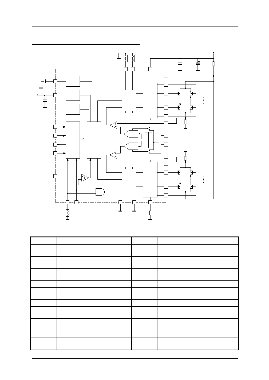
Application Circuit / Block Diagram
R
S
R
SH
Coil A
+V
M
R
S
Coil B
100µF
220nF
N
N
N
N
P
P
P
P
TMC239A
HA1
HA2
LA2
LA1
LB1
LB2
HB2
HB1
SRB
SRA
VT
VS
4
DAC
4
DAC
INA
INB
VREF
REFSEL
PW
M-CTRL
ANN
SPE
1
0
0
1
Current Contr
o
l
l
e
d
Ga
te
D
r
iv
er
s
Current Control
l
e
d
Ga
t
e
D
r
iv
er
s
SLP
R
SLP
PW
M-CTRL
OSC
Control
&
Di
a
gnosi
s
P
a
ra
lle
l
Control
SPI
-
In
t
e
rf
ac
e
REFSEL
GND
AGND
Under-
voltage
Tem-
perature
OSC
VCC
1nF
100nF
+V
CC
SCK
SDI
SDO
CSN
BL2
BL1
[MDBN]
[PHA]
[ERR]
[PHB]
stand alone mode
[MDAN]
[...]: function in stand alone mode
ENN
VCC/2
Pin Functions
Pin Function
Pin Function
VS
Motor supply voltage
VT
Short to GND detection comparator ≠
connect to VS if not used
VCC
3.0-5.5V supply voltage for analog
and logic circuits
GND
Digital / Power ground
AGND
Analog ground (Reference for SRA,
SRB, OSC, SLP, INA, INB)
OSC
Oscillator capacitor or external clock
input for chopper
INA
Analog current control phase A
INB
Analog current control input phase B
SCK
Clock input of serial interface
SDO
Data output of serial interface (tri-
state)
SDI
Data input of serial interface
CSN
Chip select input of serial interface
ENN
Device enable (low active), and
overvoltage shutdown input
SPE
Enable SPI mode (high active). Tie to
GND for non-SPI applications
ANN
Enable analog current control via
INA and INB (low active)
SLP
Slope control resistor. Tie to GND for
fastest slope
BL1, BL2
Digital blank time select
SRA, SRB Bridge A/B current sense resistor input
HA1, HA2,
HB1, HB2
Outputs for high side P-channel
transistors
LA1, LA2,
LB1, LB2
Outputs for low side N-channel
transistors
TMC239/A DATA SHEET (V2.01 / Oct. 17th, 2003)
5
Copyright © 2003, TRINAMIC Microchips GmbH
Selecting Power Transistors
Selection of power transistors for the TMC239 depends on required current, voltage and thermal
conditions. Driving transistors directly with the TMC239 is only limited by the gate capacity of these
transistors. If the total gate charge is too high, slope time increases and leads to a higher switching
power dissipation. Typical applications can reach a current in excess of 4A, while the maximum
voltage is limited to 30V. A total gate charge of below 10nC per transistor is recommended. The table
below shows a choice of transistors which can be driven directly by the TMC239. The maximum
application current mainly is a function of cooling and environment temperature. The given values are
more conservative. Peak currents typically can be higher by a factor of 1.5 for a limited time.
List of recommended transistors
Manufacturer
and type
Package
(#Trans)
Volts N-type
Volts P-type
RDS
ON
[Ohm]
Total gate
charge [nC]
Typical maximum
application current
Siliconix
SI 7501DN
PPack
(1N,1P)
30V
30V
0.03
0.05
5.0
8.0
4000mA
Siliconix
SI 4539ADY
SO8
(1N,1P)
30V
30V
0.04
0.06
7.5
9.0
3500mA
Siliconix
SI 5504
1206-8
(1N,1P)
30V
30V
0.09
0.17
5.0
5.5
2000mA
IRF 9952
SO8
(1N,1P)
30V
30V
0.10
0.25
6.9
6.1
2500mA
IRF 7509
Micro8
(1N,1P)
30V
30V
0.11
0.20
7.8
7.5
2000mA
IRF 5851
TSOP6
(1N,1P)
20V
20V
0.09
0.14
6.0
6.0
1500mA
Siliconix
SI 1901
SOT363-6
(2P)
30V 0.48
0.8 200mA
unipolar
Fairchild Semi
FDS 8333C
SO8
(1N,1P)
30V
30V
0.08
0.13
4.7
4.1
3000mA
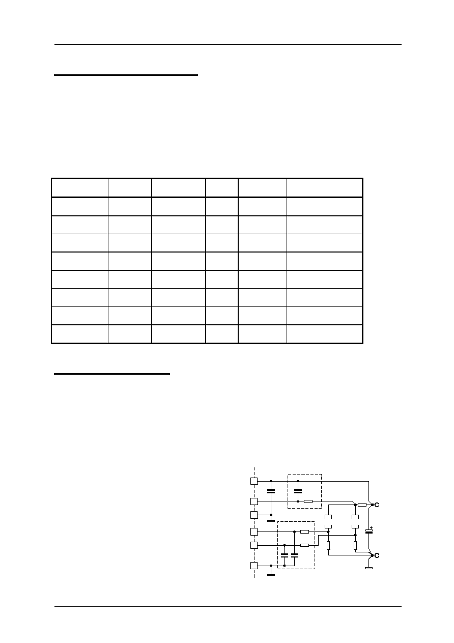
Layout Considerations
For optimal operation of the circuit a careful board layout is important, because of the combination of
high current chopper operation coupled with high accuracy threshold comparators. Please pay special
attention to massive grounding. Depending on the required motor current, either a single massive
ground plane or a ground plane plus star connection of the power traces may be used. The schematic
shows how the high current paths can be routed separately, so that the chopper current does not flow
through the system's GND-plane. Tie the TMC239's AGND and GND to the GND plane. Additionally,
use enough filtering capacitors located near to the board's power supply input and small ceramic
capacitors near to the power supply connections of the TMC239. Use low inductance sense resistors,
or add a ceramic capacitor in parallel to each resistor to avoid high voltage spikes. In some
applications it may become necessary to
introduce additional RC-filtering into the VT and
SRA / SRB line, as shown in the schematic, to
prevent spikes from triggering the short circuit
protection or the chopper comparator. If you
want to take advantage of the thermal
protection and diagnosis, ensure, that the
power transistors are very close to the
package, and that there is a good thermal
contact between the TMC239 and the external
transistors. Please be aware, that long or thin
traces to the sense resistors may add
substantial resistance and thus reduce output
current. The same is valid for the high side
shunt resistor.
+VM
GND
GND-
Plane
R
SB
R
SA
Bridge A
Bridge B
R
SH
C
VM
100R
4.7nF
optional filter
VS
VT
TMC249/
TMC239A
100R
100R
3.3 -
10nF
SRA
SRB
optional filter
AGND
GND
100nF