 | –≠–ª–µ–∫—Ç—Ä–æ–Ω–Ω—ã–π –∫–æ–º–ø–æ–Ω–µ–Ω—Ç: TA2041A | –°–∫–∞—á–∞—Ç—å:  PDF PDF  ZIP ZIP |

T r i p a t h T e c h n o l o g y, I n c . - T e c h n i c a l I n f o r m a t i o n
1
TA2041A ≠ KL/ Rev. 5.4/04.05
TA2041A
FOUR CHANNEL CLASS-T DIGITAL AUDIO AMPLIFIER USING
DIGITAL POWER PROCESSING (DPP
T M
) TECHNOLOGY
T e c h n i c a l I n f o r m a t i o n R e v i s i o n 5 . 4 ≠ A p r i l 2 0 0 5
G E N E R A L D E S C R I P T I O N
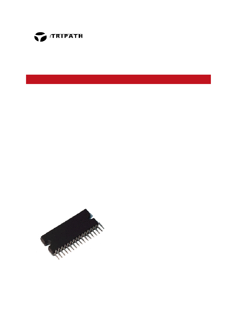
The TA2041A is a four-channel Audio Amplifier that uses Tripath's proprietary Digital Power
Processing (DPP
TM
) technology. Class-T amplifiers offer both the audio fidelity of Class-AB and the
power efficiency of Class-D amplifiers. The TA2041A has been designed specifically for automotive
head unit applications and is configured with four bridged outputs operating on a single 10-21V
supply.
A P P L I C A T I O N S
Automotive Head Units
DVD Receivers
Multimedia Speaker Systems
B E N E F I T S
4-channel (280W) solution ≠ with integrated
FETs - in a single 32-pin SSIP package
High fidelity, high efficiency Class-T
Low external component count
Single-supply operation
F E A T U R E S
Class-T architecture
Four H-Bridge outputs
"Audiophile" Sound Quality
High Efficiency
High Power @20.0V
70W
sat. sq. wave
@
4
50W @ 4
, 10% THD+N
"Audiophile" Quality Sound
0.04% THD+N @ 27W 4
0.02% IHF-IM @ 5W 4
High Efficiency
86% @ 70W 4
AM "Low EMI" mode
Pop-Free startup and shutdown
High Dynamic Range
Mute and Stand-By function
Automatic DC Offset Trim
Clip Detection Output
Protection Modes:
Output Short to VPP and Ground
Output Short across Load
Load Dump Protection
Over-/Under-Voltage Protection
Over-current Protection
Over-temperature Protection
Fortuitous Open Ground

T r i p a t h T e c h n o l o g y, I n c . - T e c h n i c a l I n f o r m a t i o n
2
TA2041A ≠ KL/ Rev. 5.4/04.05
Absolute Maximum Ratings
(Note 1)
SYMBOL PARAMETER
Value
UNITS
VPP
Supply Voltage (VPP)
26
V
VPP
MAX
Peak Supply Voltage (t<50ms) 60
V
VPP
AM
Supply Voltage in AM Mode (Note 2)
18
V
VIN
RANGE
Voltage Range for Input Section Pins (Note 3)
Inputs (Pins 1-4, 6-9)
-0.5 to 5.5
V
T
STORE
Storage Temperature Range
-55 to +150
∫C
I
R
Repetitive Peak Output Current
8
A
Tj
Maximum Junction Temperature
150
∫C
P
D
Total
Power
Dissipation
(Tcase = 70∫C)
80
W
ESD
ESD Susceptibility - Human Body Model (Note 4)
2k
V
ESD
ESD Susceptibility ≠ Machine Model (Note 5)
200
V
Note 1: Absolute Maximum Ratings indicate limits beyond which damage to the device may occur.
See the table below for Operating Conditions.
Note 2: Supply voltage is limited in AM Mode due to additional power dissipation of output stage when
operating in Class B mode. Please note that the TA2041A is still fully protected from load dump transients in AM
Mode.
Note 3
: The in
put section pins (pins 1-9, 11,12) should not be connected to voltages over 5.5V with respect to pin 10
(AGND). Please note that pins 5, 11, and 12 are outputs and can be damaged if a voltage is forced externally.
Note 4: Human body model, 100pF discharged through a 1.5K
resistor.
Note 5: Machine model, 220pF ≠ 240pF discharged through all pins.
Operating Conditions
(Note 6)
SYMBOL PARAMETER MIN.
TYP.
MAX.
UNITS
VPP
Supply Voltage (Note 6)
10
14.4
21
V
VPP
AM
Supply Voltage for AM Mode (Note 7)
10
14.4
16
V
T
A
Operating Free Air Temperature Range
-40
25
85
∫C
Note 6: Recommended Operating Conditions indicate conditions for which the device is functional.
See Electrical Characteristics for guaranteed specific performance limits.
Note 7: Supply voltage is limited in AM Mode due to additional power dissipation of output stage when
operating in Class B mode, as opposed to Switching Mode.
Thermal Characteristics
SYMBOL PARAMETER
Value
UNITS
JC
Junction-to-case Thermal Resistance
1.0
∞
C/W
JA
Junction-to-ambient Thermal Resistance (still air)
20
∞
C/W

T r i p a t h T e c h n o l o g y, I n c . - T e c h n i c a l I n f o r m a t i o n
3
TA2041A ≠ KL/ Rev. 5.4/04.05
Electrical Characteristics
(Note 8)
T
A
= 25
∞
C. Unless otherwise noted, the supply voltage is VPP=14.4V. See Application/Test Circuit.
Note 8: Minimum and maximum limits are guaranteed but may not be 100% tested.
Performance Characteristics
(Note 8)
T
A
= 25
∞
C. Unless otherwise noted, the supply voltage is VPP=14.4V, R
L
= 4
. Measurement
Bandwidth = 20kHz. See Application/Test Circuit.
SYMBOL PARAMETER
Conditions
MIN.
TYP.
MAX.
UNITS
R
IN
Input
Impedance
43 50 57
k
I
Q
Quiescent Current
No load
220
250
mA
I
STBY
Stand-By Current
V
SLEEPB
< 0.15V
100
200
µA
V
IL
Stand-By On Threshold Voltage
SLEEPB Low (amp off)
0.5
V
V
IH
Stand-By Off Threshold Voltage
SLEEPB High (amp on)
2.3
V
V
IL
Mute-On Threshold Voltage
MUTEB Low
1
V
V
IH
Mute-Off Threshold Voltage
MUTEB High
2.3
V
VOS
Output Offset Voltage
(Mute Off) DC trim active
+3 +25
mV
V
OH
Fault Reporting Logic Output High Voltage Open Drain Output
3.5
V
V
OL
Fault Reporting Logic Output Low Voltage R
FAULT
= 51K
1 V
V
IH
AM Mode On Threshold Voltage
AM pin High
2.3
V
V
IL
AM Mode Off Threshold Voltage
AM pin Low
1
V
I
AM
AM Mode Pin Input Current
1
µA
SYMBOL PARAMETER
CONDITIONS MIN.
TYP.
MAX.
UNITS
P
OUT
Output
Power
(Continuous power/ channel)
VPP=20V saturated sq. wave
VPP=20V THD+N=10%
VPP=20V THD+N=1%
VPP=16V saturated sq. wave
VPP=16V THD+N=10%
VPP=16V THD+N=1%
VPP=14.4V saturated sq. wave
VPP=14.4V THD+N=10%
VPP=14.4V THD+N=1%
65
35
72
50
40
49
33
26
39
27
21
W
W
W
W
W
W
W
W
W
A
V
Voltage Gain V
OUT
/V
IN
, R
IN
= 0
25
26
27
dB
THD + N Total Harmonic Distortion Plus
Noise
P
OUT
= 1-5W/Channel, R
L
= 4
BW = 22Hz-20kHz(AES17)
0.04
0.10 %
IHF-IM
IHF Intermodulation Distortion
19kHz, 20kHz, 1:1 (IHF)
P
OUT
= 1W/Channel
0.02
0.10
%
SNR
Signal-to-Noise Ratio
A-Weighted, P
OUT
= 50W/Channel
98
101
dB
PSRR
Power Supply Rejection Ratio
VPP=14.4V, Ripple=200mV, f= 1kHz
60
dB
Power Efficiency
Vs=20.0V, 4 x 70W sat sq wave
83
86
%
CS
Channel Separation
Po=1W, f = 1kHz
Po=1W, f = 10kHz
90
70
dB
dB
e
nOUT
Output Noise Voltage
A-Weighted
125
150
µV

T r i p a t h T e c h n o l o g y, I n c . - T e c h n i c a l I n f o r m a t i o n
4
TA2041A ≠ KL/ Rev. 5.4/04.05
AM Mode
(Note 9)
T
A
= 25
∞
C. Unless otherwise noted, the supply voltage is VPP=14.4V, R
L
= 4
. Measurement
Bandwidth = 20kHz. See Application/Test Circuit.
.
Note 9: The TA2041A heat sinking in AM Mode must be increased (as compared to Class T mode) to sustain the
typical output numbers. This is due to the lower efficiency of Class B output stage operation.
Please note that the
AM Mode operating supply range, due to this increased power dissipation, is 10V-16V.
Protection Circuits
(Note 8)
T
A
= 25
∞
C. Unless otherwise noted, the supply voltage is VPP=14.4V.
SYMBOL PARAMETER
CONDITIONS MIN.
TYP.
MAX.
UNITS
OV
ON
Over-voltage Threshold
Over-voltage turn on (amp muted)
23.0
24.0
26.0
V
OV
OFF
Over-voltage Reset
Over-voltage turn off (mute off)
22.0
22.5
V
UV
OFF
Under-voltage Reset
Under-voltage turn off (mute off)
9.5
10.0
V
UV
ON
Under-voltage Threshold
Under-voltage turn on (amp muted)
7.8
8.1
8.6
V
OT
ON
Over-Temperature Threshold
Over-temperature turn on (amp
muted)
150
160 170
∞C
OT
OFF
Over-Temperature Reset
Over-temperature turn off (mute off)
120
130 140
∞C
I
OC
Over-Current Detect
Cycle in/out of mute mode every 1s
5.5
7
A
VP
MAX
Load Dump Voltage Withstand
Test conditions, t
r
> 2.5ms,
t
pulse
<50mS
60 V
SYMBOL PARAMETER
CONDITIONS MIN.
TYP.
MAX.
UNITS
I
OCD
Over-current
detect
5.5
A
THD+N
Total Harmonic Dist plus Noise
Po=0.5-5W per channel
0.04
%
SNR
Signal to Noise ratio
A-Weighted, Po=15W
92.5
dB
Pout
Output Power (Note 7)
VPP=16V, THD+N=10%
VPP=14.4V, THD+N=10%
20
16
W
W
CS
Channel Separation
Po=1W, f=1kHz
80
dB
en
Output Noise Voltage
A-Weighted
185
µV

T r i p a t h T e c h n o l o g y, I n c . - T e c h n i c a l I n f o r m a t i o n
5
TA2041A ≠ KL/ Rev. 5.4/04.05
TA2041A Pinout
Note: The heat slug of the TA2041A is connected to PGND.
OU
T1
P
CPUMP
PG
ND34
OU
T4
N
OU
T3
N
VPP3
OU
T3
P
FAU
L
T
OU
T2
P
VPP2
OU
T2
N
IN
1
OU
T1
N
PG
ND12
VPP1
DCAP2
OU
T4
P
AG
ND2
VPPA
HMUT
EB
5VG
E
N
AG
ND1
MUTEB
O
V
RLDB
AM
SLEEPB
IN
4
IN
3
IN
2
DCAP1
32-pin SSIP Package
(Top View)
VPP4
BIASCAP
30
16
17
18
19
20
21
22
23
24
25
26
27
28
29
1
15
14
13
11
10
12
9
8
7
6
5
4
3
2
32
31


