 | –≠–ª–µ–∫—Ç—Ä–æ–Ω–Ω—ã–π –∫–æ–º–ø–æ–Ω–µ–Ω—Ç: TCD6001 | –°–∫–∞—á–∞—Ç—å:  PDF PDF  ZIP ZIP |

Tripath Technology, Inc. ≠ Preliminary Technical Information
1
TCD6001 ≠ JL/Rev. 0.9/07.05
TCD6001
6 CHANNEL CLASS-T DIGITAL AUDIO PROCESSOR USING
DIGITAL POWER PROCESSING
TM
TECHNOLOGY
General Description
The TCD6001 is a high-performance 6-channel digital audio amplifier processor. It accepts 6 digital audio
channels (3 pairs), and outputs 4 complementary single-bit digital data streams, suitable for driving Tripath
switching output stages. The other two channels of digital input are converted and routed to a stereo line-out
stage capable of driving headphones.
The TCD6001 accepts data at audio sample rates ranging from 32kHz to 192kHz and incorporates digital
interpolation and sigma-delta conversion to produce streamed digital output signals. When combined with
switching output stages, the TCD6001 allows the implementation of a complete digital audio system
incorporating Class-T Digital Audio Amplification.
Features
Class-T architecture combining ultra-low
distortion with high efficiency
Inputs support I
2
S and other PCM audio
formats
Up to 24-bit resolution (16, 18, 20, and 24
bit)
4 channel complementary output stream
capable of interfacing with various power
stages
2 channel line-out / headphone drive with
discrete digital input
Wide dynamic range
THD+N less than 0.03%
Input sampling rates up to 192kHz
I
2
C compatible interface
Seamless connection with Tripath TPS4070
or TPS4100 power stage
Low EMI AM Mode
Predictive Gain Control
Digital volume control
128dB range
1/2 dB step size in 1/8 dB increments
Zero crossing detection for click free
transitions
Automatic DC offset cancellation
Digital de-emphasis filtering for 32, 44.1 and
48kHz sampling rates
MCK
Channel HP1 & HP2
Channel 1 & 2
Channel 3 & 4
BITCK
LRCK
GAI
N
0
/
1
SC
K
SD
A
R
ESET
B
REX
T
V2
BG
VC
L
A
M
P
S
E
/
B
R
FAUL
T
HM
U
T
E
TS
T_E
N
AM
_
I
N
Y1/B
Y2/B
Y3/B
Y4/B
FB1P/N
FB2P/N
FB3P/N
FB4P/N
S
e
r
i
a
l
I
n
p
u
t
D
a
ta
P
o
r
t
Class-T Signal Processor
Class-T Signal Processor
Class-T Signal Processor
Class-T Signal Processor
Class-T Signal Processor
Class-T Signal Processor
Digital Filter Engine
Digital Filter Engine
Digital Filter Engine
Digital Filter Engine
Digital Filter Engine
Digital Filter Engine
HP1
HP2
I2C Port
Reference
Voltages
Control Signals
VPPSENSE
VNNSENSE
H
M
U
T
E_
SE
T
SL
EEPB
_
O
UT
AM
_
O
U
T
SE
/
B
R
G
B
BY
P_
CAL
O
V
RL
DB
PRELIMINARY INFORMATION
Revision 0.9≠ July 2005

Tripath Technology, Inc. ≠ Preliminary Technical Information
2
TCD6001 ≠ JL/Rev. 0.9/07.05
Absolute Maximum Ratings
(Note 1)
SYMBOL PARAMETER
Min
Max
UNITS
VD33
3.3V Digital Power Supply
-0.3
4.0
V
VA33
3.3V Analog Power Supply
-0.3
4.0
V
VA50
5V Analog Power Supply
-0.3
6.0
V
Vlogic3
Input Logic Level (DATAx, MCK, BITCLK, LRCLK, SCK,
SDA, RESET, ADDRx)
-0.3 VD33+0.3
V
Vin5
Input Level (VCLAMP, FBxx, FAULT)
-0.3
VD50+0.3
TA
Operating Free-air Temperature Range
-40
85
∞C
T
STORE
Storage Temperature Range
-55
150
∞C
T
JMAX
Maximum Junction Temperature
150
∞C
ESD
HB
ESD Susceptibility ≠ Human Body Model (Note 2) All pins
2000
V
ESD
MM
ESD Susceptibility ≠ Machine Model (Note 3) All pins
200
V
Note 1: Absolute Maximum Ratings indicate limits beyond which damage to the device may occur.
See the table below for Operating Conditions.
Note 2: Human body model, 100pF discharged through a 1.5K
resistor.
Note 3: Machine model, 220pF ≠ 240pF discharged through all pins.
Recommended Operating Conditions
(Note 4)
SYMBOL PARAMETER
MIN
TYP
MAX
UNITS
VA50
5V Analog Power Supply
4.5
5
5.5
V
VA33
3.3V Analog Power Supply
3.0
3.3
3.6
V
VD33
3.3V Digital Power Supply
3.0
3.3
3.6
V
T
A
Operating Temperature Range
-40
25
85
C
Note 4: Recommended Operating Conditions indicate conditions for which the device is functional.
See Digital, Analog, and Switching Characteristics for guaranteed specific performance limits.
Power and Thermal Characteristics
T
A
= 25
∞
C. MCK frequency is 12.288 MHz. See Application/Test Circuit on page 8.
SYMBOL PARAMETER
CONDITIONS
MIN
TYP
MAX
UNITS
PTOTAL
Total Power Dissipation
VD33 = 3.3V
VA33 = 3.3V
VA50 = 5.0V
600
mW
IA50
VA50 Power Supply Current
VA50 = 5.0V
75
100
mA
IA33
VA33 Power Supply Current
VA33 = 3.3V
50
mA
ID33
VD33 Power Supply Current
VD33 = 3.3V
20
mA
I33
Combined VD33+VA33 Power Supply
Current (Note 5)
VD33 = 3.3V
VA33 = 3.3V
100
mA
JA
Junction-to-ambient Thermal Resistance
(still air)
35
∞
C/W
Note 5: Separate IA33 and ID33 maximums are not tested.

Tripath Technology, Inc. ≠ Preliminary Technical Information
3
TCD6001 ≠ JL/Rev. 0.9/07.05
Electrical Characteristics
T
A
= 25
∞
C. Unless otherwise noted, the MCK frequency is 12.288 MHz. See Application/Test Circuit on
page 9.
SYMBOL PARAMETER
CONDITIONS MIN
TYP
MAX
UNITS
V
IH33
High-Level Input Voltage
VD33 = 3.3V
2.1
V
V
IL33
Low-Level Input Voltage
VD33 = 3.3V
0.8
V
V
OL33
Low-Level Output Voltage
VD33 = 3.0V, I
OL
= -50uA
0.1
V
VD33 = 3.0V, I
OL
= -4mA
0.44
V
V
OH5
High-Level Output Voltage
VA50 = 4.5V, I
OL
= 50uA
4.4
V
VA50 = 4.5V, I
OL
= 4mA
3.8
V
V
OL5
Low-Level Output Voltage
VA50 = 4.5V, I
OL
= -50uA
0.1
V
VA50 = 4.5V, I
OL
= -4mA
0.8
V
V
OLSLEEPB
SLEEPB Low-Level Output Voltage VA50 = 4.5V, I
OL
= -50uA
TBD
V
VA50 = 4.5V, I
OL
= -4mA
TBD
V
V
OHSLEEPB
SLEEPB High-Level Output Voltage VA50 = 4.5V, I
OL
= 50uA
TBD
V
VA50 = 4.5V, I
OL
= 4mA
TBD
V
FAULT
IH5
FAULT High-Level Trigger Voltage VA50 = 5.0V, I
FAULT
= -400uA
3.5
V
FAULT
IL5
FAULT Low-Level Trigger Voltage VA50 = 5.0V, I
FAULT
= 400uA
0.8
V
FAULT
TRIS
FAULT Tristate Leakage Limit
VA50 = 5.0V
5
5
uA
I2C
OH
I2C Tristate Leakage (SCL, SDA)
VD33 = 3.3V, V
I2C
= 3.3V
TBD
TBD
uA
V
OL33
Low-Level Output Voltage
VD33 = 3.0V, I
OL
= -50uA
TBD
V
VD33 = 3.0V, I
OL
= -4mA
TBD
V
I
VPPSENSE
VPPSENSE Threshold Currents
Over-voltage turn on (muted)
Over-voltage recover (mute off)
Under-voltage recover (mute off)
Under-voltage turn on (muted)
95
36
112
109
44
41.5
125.5
50
µ
A
µ
A
µ
A
µ
A
V
VPPSENSE
Threshold Voltages with
R
VPP1
= R
VPP2
= 576K
(Note 6)
Over-voltage turn on (muted)
Over-voltage recover (mute off)
Under-voltage recover (mute off)
Under-voltage turn on (muted)
54.7
20.7
64.5
62.8
25.3
23.9
72.3
28.8
V
V
V
V
I
VNNSENSE
VNNSENSE Threshold Currents
Over-voltage turn on (muted)
Over-voltage recover (mute off)
Under-voltage recover (mute off)
Under-voltage turn on (muted)
91
32
109
106
40.5
38
123.5
46.5
µ
A
µ
A
µ
A
µ
A
V
VNNSENSE
Threshold Voltages with
R
VNN1
= 576K
R
VNN2
= 1.74M
(Note 6)
Over-voltage turn on (muted)
Over-voltage recover (mute off)
Under-voltage recover (mute off)
Under-voltage turn on (muted)
52.4
18.4
62.8
61.1
23.3
21.9
71.1
26.8
V
V
V
V
Note 6: These supply voltages are calculated using the I
VPPSENSE
and I
VNNSENSE
values shown in the
Electrical Characteristics table. The typical voltage values shown are calculated using R
VPP
and
R
VNN
values without any tolerance variation. The minimum and maximum voltage limits shown
include either a +1% or ≠1% (+1% for Over-voltage turn on and Under-voltage turn off, -1% for Over-
voltage turn off and Under-voltage turn on) variation for RVPP1 or RVNN1 off the nominal 576k
value. These voltage specifications are examples to show both typical and worst case voltage
ranges for the given R
VPP
and R
VNN
resistor values. Please refer to the Application Information
section for a more detailed description of how to calculate the over and under voltage trip voltages
for a given resistor value.

Tripath Technology, Inc. ≠ Preliminary Technical Information
4
TCD6001 ≠ JL/Rev. 0.9/07.05
Performance Characteristics
T
A
= 25
∞
C. Unless otherwise noted, the power stage used for testing is the TPS4100, the supply voltage is
VPP=20V, R
L
= 4
, PGC = 1, post-gain = +2.5dB, coarse gain = 4x, channel volume = 255, feedback
resistor values (1% tolerance) are RFB2 = 1.0K and RFB3 = 5.6K, the MCK frequency is 12.288 MHz, fs =
48kHz, the input frequency is 1kHz, and the measurement bandwidth is 20kHz. See Application/Test Circuit
on page 9.
SYMBOL
PARAMETER
CONDITIONS
MIN TYP MAX UNITS
P
OUT
Output Power (Note 7)
(Continuous power / channel)
THD+N = 0.1%
THD+N = 1.0%
THD+N = 10%
saturated sq. wave
30
40
51
74
W
W
W
W
THD + N
Total Harmonic Distortion Plus Noise P
OUT
= 20W/Channel
0.02 0.1
%
IHF-IM
IHF Intermodulation Distortion
19kHz, 20kHz, 1:1 (IHF),
P
OUT
= 10W/Channel
0.02
0.1 %
SNR Signal-to-Noise
Ratio
A-Weighted
P
OUT
= 70W/Channel
101 dB
CS
Channel Separation
0dBr = 1W
70
80
dB
A
VERROR
Gain
Error
P
OUT
= 1W/Channel
Same chip, channel to channel
Chip to chip
0.5
TBD
0.5
TBD
dB
dB
e
NOUT
Output Noise Voltage
A-Weighted
150 180
µ
V
V
OFFSET
Output Offset Voltage
After automatic DC calibration
TBD
TBD
mV
Note 7: Typical output power performance shown for reference only. Please refer to TPS4100 data sheet
for additional information.
AM Mode Performance Characteristics
(Note 9)
T
A
= 25
∞
C. Unless otherwise noted, the power stage used for testing is the TPS4100, the supply voltage is
VPP=20V, R
L
= 4
, PGC = 1, post-gain = +2.5dB, coarse gain = 4x, channel volume = 255, feedback
resistor values are RFB2 = 1.0K and RFB3 = 5.6K, the MCK frequency is 12.288 MHz, fs = 48kHz, the input
frequency is 1kHz, and the measurement bandwidth is 20kHz. See Application/Test Circuit on page 9.
SYMBOL
PARAMETER
CONDITIONS
MIN TYP MAX UNITS
P
OUT
Output Power (Notes 7,8)
(continuous RMS/Channel)
VDD = 14.4V, THD+N = 0.1%
VDD = 14.4V, THD+N = 10%
10
16
W
W
THD + N
Total Harmonic Distortion Plus Noise P
OUT
= 1W/Channel
0.02 0.1
%
SNR
Signal-to-Noise Ratio
A-Weighted,
P
OUT
= 15W/Channel
92 94 dB
CS
Channel Separation
0dBr = 1W
70
80
dB
e
NOUT
Output Noise Voltage
A-Weighted
145 175
µ
V
V
OFFSET
Output Offset Voltage
After automatic DC calibration
TBD
TBD
mV
Note 8: Power stage heat sinking in AM Mode must be increased (as compared to Class T mode) to sustain
the typical output numbers. This is due to the lower efficiency of Class B output stage operation.

Tripath Technology, Inc. ≠ Preliminary Technical Information
5
TCD6001 ≠ JL/Rev. 0.9/07.05
Switching Characteristics
T
A
= 25
∞
C. Unless otherwise specified, VA50 = 5.0V, VD33 = 3.3V, VA33 = 3.3V.
SYMBOL PARAMETER
CONDITIONS MIN
TYP
MAX
UNITS
f
MCK0
d
MCK0
f
MCK1
d
MCK
Master Clock Timing
Frequency
Duty Cycle
Frequency
Duty Cycle
HFR bit = 0
HFR bit = 0
HFR bit = 1
HFR bit = 1
8.192
TBD
16.384
TBD
12.288
TBD
24.576
TBD
MHz
%
MHz
%
d
BITCKL
t
BITCKH
t
DATAset
t
DATAhold
I2S Control Interface Timing
BITCK Pulse Width Low
BITCK Pulse Width High
DATA Setup Time
DATA Hold Time
See section titled "Digital
Input Format".
TBD
TBD
TBD
TBD
ns
ns
ns
ns
f
SCK
t
SCKL
t
SCKH
t
SDAset
t
SDAhold
t
SDA rise
t
SDAfall
I2C Control Interface Timing
SCK Frequency
SCK Pulse Width Low
SCK Pulse Width High
SDA Setup Time
SDA Hold Time
SDA Rise Time
SDA Fall Time
0
1.3
0.6
100
90
400
300
300
KHz
us
us
ns
ns
ns
ns

Tripath Technology, Inc. ≠ Preliminary Technical Information
6
TCD6001 ≠ JL/Rev. 0.9/07.05
TCD6001 Pin Layout
1
2
3
4
5
6
7
8
9
10
11
12
13
14
15
16
17
18
19
20
21
22
23
24
25
26
27
28
29
30
31
32
33
34
35
36
37
38
39
40
41
42
43
44
45
46
47
48
49
50
51
52
53
54
55
56
57
58
59
60
61
62
63
64
65
66
67
68
69
70
71
72
73
74
75
76
77
78
79
80
81
82
83
84
85
86
87
88
89
90
91
92
93
94
95
96
97
98
99
100
VNNSENSE
GA
FB1N
FB1P
NC
NC
FB2P
FB2N
FAULT
FB3N
FB3P
FB4P
FB4N
AM_OUT
HMUTE
Y4B
Y4
Y3B
Y3
Y2B
Y2
NC
NC
Y1B
Y1
NC
NC
SLEEPB_OUT
GA
HMUTE_SET
O
V
RLDB
TST_
EN
BYP_CAL
VA50
GA5
0
AM_IN
SE/BRGB
GAIN
0
GAIN
1
TEST
NC
GA
VA33
VA33
NC
GA
GA
GD
VD18CAP
VD33
TEST
NC
NC
NC
NC
GA
GA
TEST
TEST
GD
MCK
SCK
SDA
DATA12
DATA34
DATAHP
BITCK
LRCK
VD18EN
RESETB
TESTMODE
ADDR2
TEST
ADDR1
GD
GA
NC
NC
TEST
TEST
TEST
VD33
VD18CAP
GD
GA
GA
REXT
V2BGFILT
VA33
GA
NC
NC
V2BG
HP1
HP2
GA5
0
VA50
VCLAMP_SE
VCLAMP_BR
VPPSENSE

Tripath Technology, Inc. ≠ Preliminary Technical Information
7
TCD6001 ≠ JL/Rev. 0.9/07.05
TCD6001 Pin Description
Pin Function
Type
Description
1
VNNSENSE
Input
Overvoltage and Undervoltage sensing for the VNN supply.
2 GA
Ground
Analog
Ground
3 FB1N
Input
Switching
feedback
4 FB1P
Input
Switching
feedback
5
NC
Float
Not internally connected
6
NC
Float
Not internally connected
7 FB2P
Input
Switching
feedback
8 FB2N
Input
Switching
feedback
9
FAULT
Input
3-level digital input to detect power stage fault condition
10 FB3N
Input
Switching
feedback
11 FB3P
Input
Switching
feedback
12 FB4P
Input
Switching
feedback
13 FB4N
Input
Switching
feedback
14
AM_OUT
5V Logic Output
Used to activate AM mode on external power stage
15
HMUTE
5V Logic Output
Indicates processor channels are muted. Polarity is selectable.
16
Y4B
5V Logic Output
Switching modulator output
17
Y4
5V Logic Output
Switching modulator output
18
Y3B
5V Logic Output
Switching modulator output
19
Y3
5V Logic Output
Switching modulator output
20
Y2B
5V Logic Output
Switching modulator output
21
Y2
5V Logic Output
Switching modulator output
22
NC
Float
Not internally connected
23
NC
Float
Not internally connected
24
Y1B
5V Logic Output
Switching modulator output
25
Y1
5V Logic Output
Switching modulator output
26
NC
Float
Not internally connected
27
NC
Float
Not internally connected
28
SLEEPB_OUT
5V Logic Output
Digital Output used to activate sleep mode on external power stage
29 GA
Ground
Analog
Ground
30
HMUTE_SET
5V Logic Input
Determines the state of HMUTE (pin 15) during a fault condition. If
HMUTE_SET is cleared to 0, the HMUTE will be low during a fault
condition. If HMUTE_SET is set to 1, then HMUTE will be high during a
fault condition.
31
OVRLDB
5V Logic Output
Indicates that one or more channels are near saturation
32
TST_EN
5V Logic Output
Digital output to put power stage in to test mode. Can be used as a
general purpose I/O during normal operation.
33
BYP_CAL
5V Logic Input
If BYP_CAL is set to 1, the automatic DC calibration function is disabled.
If BYP_CAL is set to 0, the DC calibration function is performed at startup.
34
VA50
Power
5V analog power supply
35
GA50
Ground
Analog ground for VA50
36
AM_IN
5V Logic Input
If AM_IN is set to 1, the system uses AM mode.
37
SE/BRGB
5V Logic Input
Sets DCB control bit power up defaults and selects VCLAMP_SE or
VCLAMP_BR
38,
39
GAIN0, GAIN1
5V Logic Input
Digital inputs which set the power up default modulator gain. GAIN0,
GAIN1=0 set the lowest gain, while GAIN0,GAIN1=1 set the highest gain
which is used for maximum output power for bridged applications.
40
TEST
Float
Test pin ≠ must be kept floating
41
NC
Float
Not internally connected
42 GA
Ground
Analog
ground
43
VA33
Power
3.3V analog power supply
44
VA33
Power
3.3V analog power supply
45
NC
Float
Not internally connected
46 GA
Ground
Analog
ground
47 GA
Ground
Analog
ground
48 GD
Ground
Digital
ground
49
VD18CAP
Output
Decoupling point for internal 1.8V regulator
50
VD33
Power
3.3V digital power supply
51
TEST
Float
Test pin ≠ must be kept floating
52
NC
Float
Not internally connected
53
NC
Float
Not internally connected
54
NC
Float
Not internally connected
55
NC
Float
Not internally connected
56 GA
Ground
Analog
ground
57 GA
Ground
Analog
ground

Tripath Technology, Inc. ≠ Preliminary Technical Information
8
TCD6001 ≠ JL/Rev. 0.9/07.05
58
TEST
Float
Test pin ≠ must be kept floating
59
TEST
Float
Test pin ≠ must be kept floating
60 GD
Power
Digital
ground
61
MCK
3.3V Logic Input
Master clock digital input
62
SCK
3.3V Logic Input
I
2
C clock input
63
SDA
3.3V Logic Input
I
2
C serial data input
64
DATA12
3.3V Logic Input
PCM audio input for channels 1 and 2
65
DATA34
3.3V Logic Input
PCM audio input for channels 3 and 4
66
DATAHP
3.3V Logic Input
PCM audio input for headphone output channels 1 and 2
67
BITCK
3.3V Logic Input
PCM audio bit clock input
68
LRCK
3.3V Logic Input
PCM audio left/right clock input
69
VD18EN
3.3V Logic Input
1.8V internal regulator enable
70
RESETB
3.3V Logic Input
Reset input ≠ resets internal registers
71
TESTMODE
3.3V Logic Input
Test mode enable ≠ must be kept grounded
72
ADDR2
3.3V Logic Input
Chip address select 2
73
TEST
Float
Test pin ≠ must be kept floating
74
ADDR1
3.3V Logic Input
Chip address select 1
75 GD
Ground
Digital
ground
76 GA
Ground
Analog
ground
77
NC
Float
Not internally connected
78
NC
Float
Not internally connected
79
TEST
Float
Test pin ≠ must be kept floating
80
TEST
Float
Test pin ≠ must be kept floating
81
TEST
Float
Test pin ≠ must be kept floating
82
VD33
Power
3.3V digital power supply
83
VD18CAP
Output
Decoupling point for internal 1.8V regulator
84 GD
Ground
Digital
ground
85 GA
Ground
Analog
ground
86 GA
Ground
Analog
ground
87
REXT
Output
Analog current reference output ≠ requires 10K ohms +/- 1% to GA
88 V2BGFILT
Output
Reference
Voltage
89
VA33
Power
3.3V analog power supply
90 GA
Ground
Analog
ground
91
NC
Float
Not internally connected
92
NC
Float
Not internally connected
93 V2BG
Output
Reference
Voltage
94
HP1
Output
Headphone amplifier output channel 1
95
HP2
Output
Headphone amplifier output channel 2
96
GA50
Ground
Analog ground for VA50
97
VA50
Power
5V analog power supply
98
VCLAMP_SE
Input
Soft clamp threshold voltage input to control audio signal clipping with
single ended stages (see SE/BRGB pin)
99
VCLAMP_BR
Input
Soft clamp threshold voltage input to control audio signal clipping with
bridged output stages (see SE/BRGB pin)
100
VPPSENSE
Input
Overvoltage and Undervoltage sensing for the VPP supply

Tripath Technology, Inc. ≠ Preliminary Technical Information
9
TCD6001 ≠ JL/Rev. 0.9/07.05
TCD6001 Connection Diagram
SLEEPB
Y3B
3.3V
VNN
Y2B
Ra
Rfb2
0.1uF
0.1uF
Rp
Rfb3
FB4P
+
Ch
100u;10V
Cs
0.1uF
Rfb3
5.0V
FB2P
PCM AUDIO
SOURCE
Rfb3
+
Ch
100u;10V
AM_MODE
Rfb2
Cs
0.1uF
FB2N
FB3P
Cs
0.1uF
Ra
Cs
0.1uF
3.3V
VPP
10
3.3V
Y4B
RVNN2
ADDRESS
VNN
Rp
RVPP1
Cs
0.1uF
I2C
CONTROL
Rfb3
Rfb3
Rd
Cs
0.1uF
Cs
0.1uF
FB1N
FB1P
10
VA50
Cv2bg
0.1uF
99
7
8
2
10
11
9
13
12
15
32
31
25
24
21
20
29
19
18
17
16
34
35
51
43
44
46
47
84
49
50
58
57
59 73
48
61
62
63
64
65
66
67
68
69
70
71
72
79
74
75
80 81
82
83
60
76
86
87
88
89
93
94
95
96
97
4
3
56
98
1
100
28
14
37
36
85
40
33
30
38
39
42
90
VCLAMP_BR
FB2P
FB2N
GA
FB3N
FB3P
FAULT
FB4N
FB4P
HMUTE
TST_EN
OVRLDB
Y1
Y1B
Y2
Y2B
GA
Y3
Y3B
Y4
Y4B
VA50
GA
T
EST
VA33
VA33
GA
GA
GD
VD18CAP
VD33
T
EST
GA
T
EST
T
EST
GD
MCK
SCK
SDA
DATA12
DATA34
DATAHP
BITCK
LRCK
VD18EN
RESETB
TESTMODE
ADDR2
T
EST
ADDR1
GD
T
EST
T
EST
VD33
VD18CAP
GD
GA
GA
REXT
V2BGFILT
VA33
V2BG
HP1
HP2
GA
VA50
FB1P
FB1N
GA
VCLAMP_SE
VNNSENSE
VPPSENSE
SLEEPB_OUT
AM_OUT
SE/BRGB
AM_IN
GA
T
EST
BYP_CAL
HMUTE_SET
GAIN0
GAIN1
GA
GA
Rb
Rfb2
Rfb3
HMUTEB
Rfb2
3.3V
5V
3.3V
RVNN1
+
4.7uF
Y3
Rb
VPP
Y2
Cs
0.1uF
Rfb2
VPP
0.1uF
RESET
FB3N
5V
RVPP2
Y1
Y4
FB4N
Ra
FAULT
Rfb3
Rext
10K 1%
Cs
0.1uF
QB
Rfb3
5V
QA
Rfb2
Connect ground planes at a
single location near
TCD6001.
3.3V
Y1B
Cv2bg
0.1uF
2
3
4
5
1
Rfb2
3.3V
5V
5V
Rfb2
AM MODE
SELECT

Tripath Technology, Inc. ≠ Preliminary Technical Information
10
TCD6001 ≠ JL/Rev. 0.9/07.05
TPS4100 Connection Diagram
VPP
Cs
0.1uF
Do
VPP
Y2B
CPUMP
close to
PIN18
FAULT
FB1P
Ccp
0.1uF
VPP
Do
VPP
Co
0.47uF
Cz
0.22uF
FB4P
Do
FB3P
Do
Lo
10uH
Cz
0.22uF
Cbr
0.1uF
RL
SLEEPB
Cbr
0.1uF
Ccp
0.1uF
Cbr
390uF
Do
Y4B
FB3N
Y1B
Cbr
0.1uF
VPP
VPP
TPS4100
1
3
4
5
6
7
8
9
10
11
12
13
14
15
16
17
18
19
20
21
22
23
24
25
26
27
28
29
30
31
32
2
SLEEPB
Y1B
Y2
Y2B
Y3
Y3B
Y4
Y4B
M
U
TEB
AM
V5G
E
N
GNDA
GNDA
CP
UMP
OUT
4
P
VPP4
PG
N
D
OUT
4
N
OUT
3
N
VPP3
OUT
3
P
FAU
LT
OUT
2
P
VPP2
OUT
2
N
OUT
1
N
PG
N
D
VPP1
OUT
1
P
D
C
AP2
PG
N
D
Y1
close to
PIN18
FB2P
Co
0.47uF
HMUTEB
Do
Do
FB1N
RL
Do
FB2N
Lo
10uH
Y3B
Do
Co
0.47uF
Rz
10;2W
VPP
close to
PIN28
VPP
Y1
Co
0.47uF
Y4
VPP
FB4N
Cz
0.22uF
close to
PIN28
Do
Cz
0.22uF
Co
0.47uF
VPP
Do
Do
Rz
10;2W
Ccp
0.1uF
RL
Do
Y3
Do
Lo
10uH
Do
Do
Lo
10uH
Rz
10;2W
Dcp
AM_MODE
Cbr
0.1uF
Dcp
Co
0.47uF
RL
VPP
Cs
3.3uF
Co
0.47uF
VPP
Y2
Rz
10;2W
Ccp
3.3uF
Co
0.47uF

Tripath Technology, Inc. ≠ Preliminary Technical Information
11
TCD6001 ≠ JL/Rev. 0.9/07.05
Typical Performance
-120
+0
-110
-100
-90
-80
-70
-60
-50
-40
-30
-20
-10
d
B
V
20
20k
50
100
200
500
1k
2k
5k
10k
Hz
Noise Floor
V
PP
= 20.0V
R
L
= 4
32k FFT
F
S
= 65kHz
BW = 22Hz - 20kHz(AES17)
-130
+0
-120
-110
-100
-90
-80
-70
-60
-50
-40
-30
-20
-10
d
B
r
A
20
30k
50
100
200
500
1k
2k
5k
10k
20k
Hz
Intermodulation Distortion
19kHz, 20kHz 1:1
P
O
= 1W
V
PP
= 20.0V
R
L
= 4
32k FFT
F
S
= 65kHz
BW = <10Hz - 80kHz
0.001
1
0.002
0.005
0.01
0.02
0.05
0.1
0.2
0.5
%
10
20k
20
50
100
200
500
1k
2k
5k
10k
H z
THD+N versus Frequency
P
O
= 1W
V
PP
= 20.0V
R
L
= 4
BW = 30kHz
BW = 22kHz
0.001
1
0.002
0.005
0.01
0.02
0.05
0.1
0.2
0.5
%
10
20k
20
50
100
200
500
1k
2k
5k
10k
H z
THD+N versus Frequency
P
O
= 1W
V
PP
= 20.0V
R
L
= 8
BW = 30kHz
BW = 22kHz
-110
+0
-100
-90
-
80
-70
-60
-50
-40
-30
-20
-10
d
B
r
A
20
20k
50
100
200
500
1k
2k
5k
10k
Hz
T
T
T
T
T
T
T
T
T
T
T
T
T
T
T
T
T
T
T
T
T
T
T
T
T
Channel Separation
V
PP
= 20V
R
L
= 4
P
O
= 1W
BW = 22Hz - 22kHz

Tripath Technology, Inc. ≠ Preliminary Technical Information
12
TCD6001 ≠ JL/Rev. 0.9/07.05
Typical Performance (continued)
0.001
1
0.002
0.00
5
0.01
0.02
0.05
0.1
0.2
0.5
%
10
20k
20
50
100
200
500
1k
2k
5k
10k
Hz
THD+N versus Frequency
AM MODE
P
O
= 1W
V
PP
= 14.4V
R
L
= 4
BW = 30kHz
BW = 22kHz
-110
+0
-100
-90
-80
-70
-60
-50
-40
-30
-20
-10
d
B
r
A
20
20k
50
100
200
500
1k
2k
5k
10k
H z
Channel Separation
AM MODE
V
PP
= 14.4V
R
L
= 4
P
O
= 1W
BW = 22Hz - 22kHz

Tripath Technology, Inc. ≠ Preliminary Technical Information
13
TCD6001 ≠ JL/Rev. 0.9/07.05
TCD6001 Operation Overview
POWER SUPPLY
The TCD6001 requires both 3.3V and 5V supplies. Pins labeled VD33 correspond to the digital power
networks, and pins labeled VA33 and VA50 correspond to the analog power networks. All should be
separately decoupled to their respective grounds.
All TCD6001 logic inputs are 3.3V unless otherwise specified.
VD18EN
VD18EN is a logic input that enables the internal 1.8V regulator. It should be tied to VD33.
REXT
The REXT pin should be connected to ground through an external 10K
. This connection is used by the
TCD6001 as a current reference. The 10K
resistor must have an accuracy of +/- 1%.
V2BG and V2BGFILT
The V2BG and V2BGFILT pin should each be AC coupled to GA with a 0.1uF capacitor.
RESETB
When pulled low, the RESETB pin will force all control registers from sub-address 00h to 6Fh and 80h to
EFh to their default state. Registers from sub-address 70h to 7Fh and F0h to FFh remain unchanged.
FAULT
The TCD6001 has the ability to detect Over and Under-voltage faults via external sense resistors. The
TCD6001 does not detect over current or over temperature faults. These are expected to be done
externally. However, a FAULT input has been provided as an alternate "mute" input. The default (non-
muted) state for FAULT is "floating". The pin will self-bias to approximately 2.5V. If FAULT is taken to either
5V or 0V the TCD6001 will go in to hard mute. If FLD (register 3Ah bit D2) is set to `1', the TCD6001 will
automatically un-mute after FAULT is released (forced or floated back to 2.5V). If FLD is cleared to `0', the
TCD6001 will remain latched in this FAULT-based muted condition until the FAULT pin is released and FLC
(register 3Ah bit D1) undergoes a `0' to `1' transition.
AUTOMATIC DC OFFSET CALIBRATION
When the TCD6001 comes out of hard mute (register 2Ch bit D1 transitions from `1' to `0') an automatic DC
offset calibration sequence is started. During this sequence, the TCD6001 calibrates itself and its external
components to minimize DC offset at the speaker outputs that can be caused by process variations and
component tolerance.
The automatic DC offset calibration sequence takes a maximum of 1 second if the PGC is disabled and 4
seconds if the PGC is enabled. The additional time is required because each different amplifier gain level
may require a different calibration level. Therefore, each of the four PGC levels will require calibration upon
un-muting.
Automatic DC offset calibration produces 10 bit offset values for each channel that are stored in internal
registers. When Automatic DC offset calibration is enabled, the 10 bit values that are in use can be read in
the Calibration Readback registers (registers 02h ≠ 09h). When the PGC is enabled, four different values
are stored for each channel. The values that are seen in the Calibration Readback registers will change as
the PGC Setting changes.

Tripath Technology, Inc. ≠ Preliminary Technical Information
14
TCD6001 ≠ JL/Rev. 0.9/07.05
AM MODE
The TCD6001 is typically configured as a high power, high efficiency, four channel switching amplifier. The
TCD6001 also has an additional amplifier mode named "AM Mode." When used with a Tripath Technology
power stage also equipped with AM Mode, the TCD6001 can be configured as a Class B amplifier as
opposed to the normal Class T amplifier by pulling the AM_IN pin to a logic high level.
AM mode significantly reduces EMI generation since the output amplifiers are now operated in linear mode.
Operating in Class B mode also reduces the power stage's efficiency especially at low to medium output
powers. Due to this increased power dissipation, it is recommended that the AM mode is used for
applications such as AM radio playback where the average output level is minimal and a switching amplifier
would most effect radio reception.
PREDICTIVE GAIN CONTROL
The Predictive Gain Control (PGC) automatically sets one of four different pre-gain levels depending on the
Channel Volume level (registers 25h ≠ 2Ah). The PGC allows less gain to be used for lower volume levels.
This results in greater digital resolution and lower noise floor. When PGC is enabled (register 3Dh bit D7 is
set to `1'), PGC settings are changed automatically by the Channel Volume. When PGC is disabled, the
system's pre-gain level is always set to full gain.
Channel Volume Range
PGC Setting
FFh ≠ F4h
Full Gain
F3h ≠ E8h
1/2 Gain
E7h ≠ DCh
1/4 Gain
DBh ≠ 00h
1/8 Gain
POST-GAIN
The TCD6001 has four "post-gain" settings: -6.5dB, -3.5dB, 0dB, and +2.5dB. A post-gain setting of 0dB is
considered nominal and allows the power stage to achieve rail to rail clipping of approximately 10% THD.
Post-gain settings of ≠6.5dB and ≠3.5 dB have lower noise floor but the TCD6001 may clip internally before
the power stage reaches its own clipping points ≠ reducing maximum output power. A post-gain setting of
+2.5dB allows for extreme clipping at the power stage outputs at the cost of a higher noise floor.
The user may use low post-gain at low volume levels to take advantage of the lower noise floor and use high
post-gain at higher volume levels to take advantage of the full range of the power stage. Precautions must
be taken while changing post-gain to prevent DC offset. The automatic DC offset cancellation settings will
have been affected by changes in post-gain. To avoid this problem, the software that is controlling the
TCD6001 through the I
2
C port should store DC calibration values for each post-gain setting and swap
between them as in the following procedure:
1. Set post-gain to low and channel volumes to 00h.
2. Un-mute.
3. Wait for calibration to complete.
4. Read values in the "Calibration Readback" registers and write them to the "Calibration Bank"
registers.
5. Mute.
6. Set post-gain to high and channel volumes to 00h.
7. Un-mute.
Now the calibration bank contains the DC calibration values for low post-gain and the TCD6001 has stored
the DC calibration values for high post-gain in its internal registers. When the CFn bits (register 2Fh bits
D5..D0) are set to `1', the values stored in the Calibration Bank are used. When the CFn bits are cleared to
`0', the internal registers that hold the automatic DC calibration values for high post-gain are used. If the
PGC is enabled, the software should only switch between low and high post-gain modes when the PGC is in
1/8 Gain mode. This is because the values stored in the Calibration Bank will only be valid for the PGC
mode that was in effect when the channel volumes were set to 00h and automatic DC calibration took place.

Tripath Technology, Inc. ≠ Preliminary Technical Information
15
TCD6001 ≠ JL/Rev. 0.9/07.05
Special care should be taken when using this scheme to prevent events from interfering with DC calibration.
FAULT should be latched so that a proper calibration can take place during un-mute. Clocks should be kept
synchronized to prevent automatic reset.
I
2
C INTERFACE
The I
2
C interface is a simple bi-directional bus interface for allowing a microcontroller to read and write
control registers in the TCD6001. Every component hooked up to the I
2
C bus has its own unique address
whether it is a CPU, memory or some other complex function chip. Each of these chips can act as a receiver
and/or transmitter depending on its functionality. The TCD6001 acts as a slave while a microcontroller would
act as a master.
The TCD6001 device address is 80h, 82h, 84h, or 86h depending on the state of the ADDRn pins. The
TCD6001 constantly monitors the I
2
C data input and waits until its device address appears before writing
into or reading from its control registers. The 8
th
bit of the address determines whether the master is reading
or writing. When the last bit is HIGH, the master is reading from a register on the slave. When the last bit is
LOW, the master is writing to a register on the slave.
ADDR2 ADDR1 TCD6001
write
address
TCD6001 read
address
0 0 80h
81h
0 1 82h
83h
1 0 84h
85h
1 1 86h
87h
The I
2
C interface consists of a serial data input (SDA) and a clock input (SCK) and is capable of both
reading and writing. Both SCK and SDA are bi-directional lines connected to VD33 via a pull-up resistor.
When the bus is free both lines are HIGH.
The SCK clock frequency is typically less than 400 kHz. Data is transmitted serially in groups of 8 bits,
followed by an acknowledge bit. The data on the SDA line is expected to be stable while SCK is HIGH.
start
stop
A7
A6
A5
A4
A3
A2
A1
R/W
D7
D6
D5
D4
D3
D2
D1
D0
ACK
ACK
SCK
SDA
A START condition is defined as a HIGH to LOW transition on the data line while the SCL line is held HIGH.
After this has been transmitted by the master, the bus is considered busy. The next byte of data transmitted
after the start condition contains the address of the slave in the first 7 bits and the eighth bit tells whether the
master is receiving data from the slave or transmitting data to the slave. When an address is sent, each
device in the system compares the first seven bits after a start condition with its address. If they match, the
device considers itself addressed by the master. Data transfer with acknowledge is obligatory. The
transmitter must release the SDA line during the acknowledge pulse. The receiver must then pull the data
line LOW so that it remains stable low during the HIGH period of the acknowledge clock pulse. A receiver
which has been addressed is obliged to generate an acknowledge after each byte of data has been
received. The receiver can hold the SCK line LOW after an acknowledge to force the transmitter to wait until
the receiver is ready to accept another byte.
When addressed as a slave, the following protocol must be adhered to, once a slave acknowledge has been
returned, an 8-bit sub-address will be transmitted. If the LSB of the slave address was `1', a repeated
START condition will have to be issued after the address byte; if the LSB is `0' the master will transmit to the
slave with direction unchanged.
When the master writes data to the slave, the following events occur:
0. SDA and SCK are both HIGH.
1. A start condition is generated when the master pulls SDA LOW.
2. The master begins toggling SCK and transmits the slave's device address on SDA with a 0 in
the LSB (ex. 80h).

Tripath Technology, Inc. ≠ Preliminary Technical Information
16
TCD6001 ≠ JL/Rev. 0.9/07.05
3. On the ninth SCK pulse, the master releases SDA and the slave acknowledges by pulling SDA
LOW.
4. The slave holds SCK low until it is ready to receive the next byte.
5. The slave releases SCK and the master begins toggling SCK and transmits the control register
address on SDA.
6. On the ninth SCK pulse, the master releases SDA and the slave acknowledges by pulling SDA
LOW.
7. The slave holds SCK low until it is ready to receive the next byte.
8. The slave releases SCK and the master begins toggling SCK and transmits the data byte on
SDA.
9. On the ninth SCK pulse, the master releases SDA and the slave acknowledges by pulling SDA
LOW.
10. The slave holds SCK low until it is ready to receive the next byte.
11. To transmit additional data bytes, repeat steps 8 through 10.
12. A stop condition is generated when SCK is released and SDA goes HIGH while SCK is still
high.
When the master reads data from the slave, the following events occur:
0. SDA and SCK are both HIGH.
1. A start condition is generated when the master pulls SDA LOW.
2. The master begins toggling SCK and transmits the slave's device address on SDA with a 1 in
the LSB (ex. 81h).
3. On the ninth SCK pulse, the master releases SDA and the slave acknowledges by pulling SDA
LOW.
4. The slave holds SCK low until it is ready to receive the next byte.
5. The slave releases SCK and the master begins toggling SCK and transmits the control register
address on SDA.
6. On the ninth SCK pulse, the master releases SDA and the slave acknowledges by pulling SDA
LOW.
7. The slave holds SCK low until it is ready to transmit data.
8. The slave releases SCK and the master begins toggling SCK and the slave transmits the data
byte on SDA.
9. On the ninth SCK pulse, the slave releases SDA and the master acknowledges by pulling SDA
LOW.
10. The slave holds SCK low until it is ready to transmit the next byte.
11. To read additional data bytes, repeat steps 8 through 10.
12. A stop condition is generated when SCK is released and SDA goes HIGH while SCK is still
high.
When writing to the TCD6001, the first data byte after the device address is a sub-address. Subsequent
data will be written to TCD6001 control registers referred to by the sub-address. When reading from the
TCD6001, data will be read starting from the most recently written sub-address.
Control registers from sub-addresses 00h through 7Fh can also be accessed at sub-addresses 80h through
FFh. The difference is that sub-addresses 80h through FFh are auto-increment registers. Repeated reads
and writes to these registers will automatically increment the sub-address.
For example, if a microcontroller wanted to write a value of E6h to all of the volume registers, it would write
the following bytes through its I
2
C port: <start> 80h A5h E6h E6h E6h E6h E6h E6h <stop>. If it wanted to
read those values back it would send: <start> 80h A5h <stop> <start> 81h <read> <read> <read> <read>
<read> <read> <stop>.

Tripath Technology, Inc. ≠ Preliminary Technical Information
17
TCD6001 ≠ JL/Rev. 0.9/07.05
Control Registers
This section describes the user-programmable registers controlling many features of the TCD6001. They are
programmed using the I
2
C interface.
Control bits shown in gray are for Tripath use only and should be set to the values shown. All registers not
shown are reserved and should not be changed.
Control Register Mapping
Sub-Addr
Register
Name
D7 D6 D5 D4 D3 D2 D1 D0
00h Mute
Status
0
0
0
MUS SMU FMU HMU AMU
01h Volume
Status
0
0
VZH2 VZH1 VZ4 VZ3 VZ2
VZ1
02h
Calibration
Readback CR19 CR18 CR17 CR16 CR15 CR14 CR13 CR12
03h
Calibration
Readback CR29 CR28 CR27 CR26 CR25 CR24 CR23 CR22
04h
Calibration
Readback CR39 CR38 CR37 CR36 CR35 CR34 CR33 CR32
05h Calibration
Readback
0
0
CR31 CR30 CR21 CR20 CR11 CR10
06h
Calibration
Readback CR49 CR48 CR47 CR46 CR45 CR44 CR43 CR42
07h Calibration
Readback
0
0
0
0
0
0
0
0
08h Calibration
Readback
0
0
0
0
0
0
0
0
09h Calibration
Readback
0
0
0
0
0
0
CR41 CR40
20h Freeze
Control
0
0
0
0
0
0
0
CHG
21h
Filter Bypass Control
DCB
DEB
DRB
0
0
0
0
0
22h
Sampling Rate Control
0
0
0
1Xf 1Xs 0
S4X S2X
23h Operation
Control
0
1
0
0
HFR
0
R1 R0
24h
Digital Input Format
0
DP BCK CCK I2S DA DW1 DW0
25h
Channel
1
Volume V17 V16 V15 V14 V13 V12 V11 V10
26h
Channel
2
Volume V27 V26 V25 V24 V23 V22 V21 V20
27h
Channel
3
Volume V37 V36 V35 V34 V33 V32 V31 V30
28h
Channel
4
Volume V47 V46 V45 V44 V43 V42 V41 V40
29h
Channel
HP1
Volume VH17 VH16 VH15 VH14 VH13 VH12 VH11 VH10
2Ah
Channel
HP2
Volume VH27 VH26 VH25 VH24 VH23 VH22 VH21 VH20
2Bh
Volume
Ramp
Rate RR7 RR6 RR5 RR4 RR3 RR2 RR1 RR0
2Ch
Channel Mute Control
MH2
MH1
M4
M3
M2
M1
HM
AM
2Dh
Auto-Mute
Timing AM7 AM6 AM5 AM4 AM3 AM2 AM1 AM0
2Eh Volume
Change
Control
0
0
0
0
VR1 VR0 VRE ZCE
2Fh
DC Calibration Control
0
CAB CFH2
CFH1 CF4 CF3 CF2 CF1
30h Calibration
Bank
CB19
CB18
CB17 CB16 CB15 CB14 CB13 CB12
31h Calibration
Bank
CB29
CB28
CB27 CB26 CB25 CB24 CB23 CB22
32h Calibration
Bank
CB39
CB38
CB37 CB36 CB35 CB34 CB33 CB32
33h Calibration
Bank
0
0
CB31 CB30 CB21 CB20 CB11 CB10
34h Calibration
Bank
CB49
CB48
CB47 CB46 CB45 CB44 CB43 CB42
35h
Calibration
Bank
CH19 CH18 CH17 CH16 CH15 CH14 CH13 CH12
36h
Calibration
Bank
CH29 CH28 CH27 CH26 CH25 CH24 CH23 CH22
37h Calibration
Bank
0
0
CH21 CH20 CH11 CH10 CB41 CB40
38h
Force
DC
FD7 FD6 FD5 FD4 FD3 FD2 FD1 FD0
39h
Dither
Control
DT7 DT6 DT5 DT4 DT3 DT2 DT1 DT0

Tripath Technology, Inc. ≠ Preliminary Technical Information
18
TCD6001 ≠ JL/Rev. 0.9/07.05
3Ah
Fault Latch Control
0
0
0
0
0
FLD FLC 0
3Bh
Saturation Clamp LSB
1
1
1
1
1
1
1
1
3Ch
Saturation Clamp MSB
1
1
1
0
0
1
1
1
3Dh
Predictive Gain Control
PGC
0
0
0
0
0
0
0
71h
Output
Delay
Control YD23 YD22 YD21 YD20 YD13 YD12 YD11 YD10
72h
Output
Delay
Control YD43 YD42 YD41 YD40 YD33 YD32 YD31 YD30
73h
Startup Burst Control
0
0
0
0
0
0
STB1 STB0
74h Headphone
and
Logic
0
YSN HPO TO
0
0
0
0
75h Test
0
0
0
0
0
0
0
0
76h Output
Timing
Control
DEL
DCB
DCX
0
HMF BB2 BB1 BB0
77h
Individual Hard Mute
0
HM4 HM3 HM2 HM1 0
0
0
78h Test
0
0
0
0
0
0
0
0
79h Test
0
0
0
0
0
0
0
0
7Ah
Gain
Control
GN41 GN40 GN31 GN30 GN21 GN20 GN11 GN10
7Bh Test
0
0
0
0
0
0
0
0
7Ch
OV and SLEEPB control
0
0
SLPB OVDB 0
0
0
0
7Dh B-Cal
Control
0
0
0
BC4 BC3 BC2 BC1 0

Tripath Technology, Inc. ≠ Preliminary Technical Information
19
TCD6001 ≠ JL/Rev. 0.9/07.05
Mute Status
Addr
Register
Name
D7 D6 D5 D4 D3 D2 D1 D0
00h Mute
Status 0
0
0
MUS SMU FMU HMU AMU
Default
0
0
0
0 0 0 0 0
This is a read only register that indicates the status of various mute conditions. A `1' indicates that that
particular mute is active. MUS indicates that a mute has occurred. Bits D0 through D3 indicate what kind of
mute has occurred.
AMU = Auto Mute
HMU = Hard Mute
FMU = Fault Mute
SMU = Sync Mute
Volume Status
Addr
Register
Name
D7 D6 D5 D4 D3 D2 D1 D0
01h Volume
Status 0
0
VZH2 VZH1 VZ4 VZ3 VZ2
VZ1
Default
0
0
0 0 0
0 0
0
These are read only bits that are set to `1' when their respective volume registers are cleared to 0. For
example, when register 27h has a value of 8Ch, VZ3 is cleared to `0'. When register 27h has a value of 00h,
VZ3 is set to `1'.
Calibration Readback
Addr
Register
Name
D7 D6 D5 D4 D3 D2 D1 D0
02h
Calibration
Readback
CR19 CR18 CR17 CR16 CR15 CR14 CR13 CR12
03h
Calibration
Readback
CR29 CR28 CR27 CR26 CR25 CR24 CR23 CR22
04h
Calibration
Readback
CR39 CR38 CR37 CR36 CR35 CR34 CR33 CR32
05h Calibration
Readback 0
0
CR31 CR30 CR21 CR20 CR11 CR10
06h
Calibration
Readback
CR49 CR48 CR47 CR46 CR45 CR44 CR43 CR42
07h Calibration
Readback 0
0
0
0
0
0
0
0
08h Calibration
Readback 0
0
0
0
0
0
0
0
09h Calibration
Readback 0
0
0
0
0
0
CR41 CR40
Default
0 0 0 0 0 0 0 0
These read only registers show the current automatic DC calibration values. The DC calibration values are
10 bit words so they are stored in separate bytes. For example, for channel 1, the 8 most significant bits are
stored in register 02h, while the 2 least significant bits are stored in register 05h ≠ bits D1 and D0.
When PGC is enabled, four different automatic DC calibration values are stored internally ≠ one for each
PGC setting. As the channel volume is changed across PGC boundaries, the Calibration Readback value
will change to reflect the new PGC setting.
For example, if the user changes channel 1 volume from FFh down to F0h, the PGC level has changed from
"full" down to "1/2". Internally, the TCD6001 switches from the DC calibration value that it calculated for full
PGC to the DC calibration value that it calculated for 1/2 PGC. The value present in the channel 1
Calibration Readback register also changes to indicate the 1/2 PGC DC calibration value.
Tripath Technology, Inc. ≠ Preliminary Technical Information
20
TCD6001 ≠ JL/Rev. 0.9/07.05
Freeze Control
Addr
Register
Name
D7 D6 D5 D4 D3 D2 D1 D0
20h Freeze
Control 0
0
0
0
0
0
0
CHG
Default
0
0
0
0
0
0
0
0
While CHG is set to `1', any value that is written to a register takes effect immediately. However, while CHG
is cleared to `0', any changes that are made to registers 00h through 6Fh and 80h through EFh will not take
effect until CHG is set to `1'. For example, if the user wanted to set all channels to a volume of F6h at the
same time, the user could clear CHG, set registers 25h through 2Ah to F6h one at a time, then set CHG to
`1'.
Registers 70h through 7Fh and F0h through FFh are not affected by CHG.
Filter Bypass Control
Addr
Register
Name
D7 D6 D5 D4 D3 D2 D1 D0
21h
Filter Bypass Control
DCB
DEB
DRB
0
0
0
0
0
Default 0
0
0
0
0
0
0
0
This register allows users to bypass any of the 3 digital filters incorporated in the TCD6001:
DCB = DC blocking filter
DEB = De-Emphasis filter
DRB = Droop correction filter
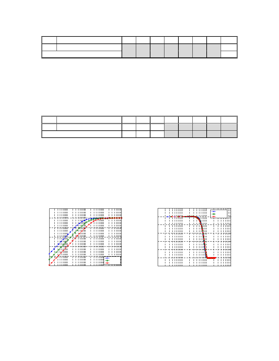
Setting these bits to `1' bypasses the corresponding filter.
The DC blocking filter eliminates the DC component in an incoming signal. The frequency response of the
DC blocking filter is shown in Figure 1 for the 1X, 2X, and 4X modes.
Figure 1. DC Blocking Filter Characteristics
Figure 2. De-Emphasis Filter Characteristics
The De-Emphasis filter is used to re-shape the frequency response and reduce gain for frequencies above
3.183 kHz. It is only available in the 1X mode. If enabled, it needs to be selected for 1 of 4 possible input
data rates (32 kHz, 44.1kHz, or 48 kHz), as specified by bits D4 and D3 in the Sampling Rate and De-
Emphasis Control Register (address 22h).
The frequency response of the De-emphasis filter is shown in Figure 2 for all 3 input data rates.
The De-Emphasis Filter Selection bit is ignored for the 2X and 4X input data-sampling modes.
10
-2
10
-1
10
0
10
1
10
2
-50
-40
-30
-20
-10
0
10
Frequency in Hz
A
tte
n
u
a
t
i
o
n i
n
d
B
Behaviour of D C Filter in Various Modes
1x mode
2x mode
4x mode
10
2
10
3
10
4
10
5
-12
-10
-8
-6
-4
-2
0
2
Frequency in Hz
A
t
t
e
n
u
a
t
i
on
i
n
dB
Spectrum of D e-emphasis Filter
32 kHz
44.1 kHz
48 kHz

Tripath Technology, Inc. ≠ Preliminary Technical Information
21
TCD6001 ≠ JL/Rev. 0.9/07.05
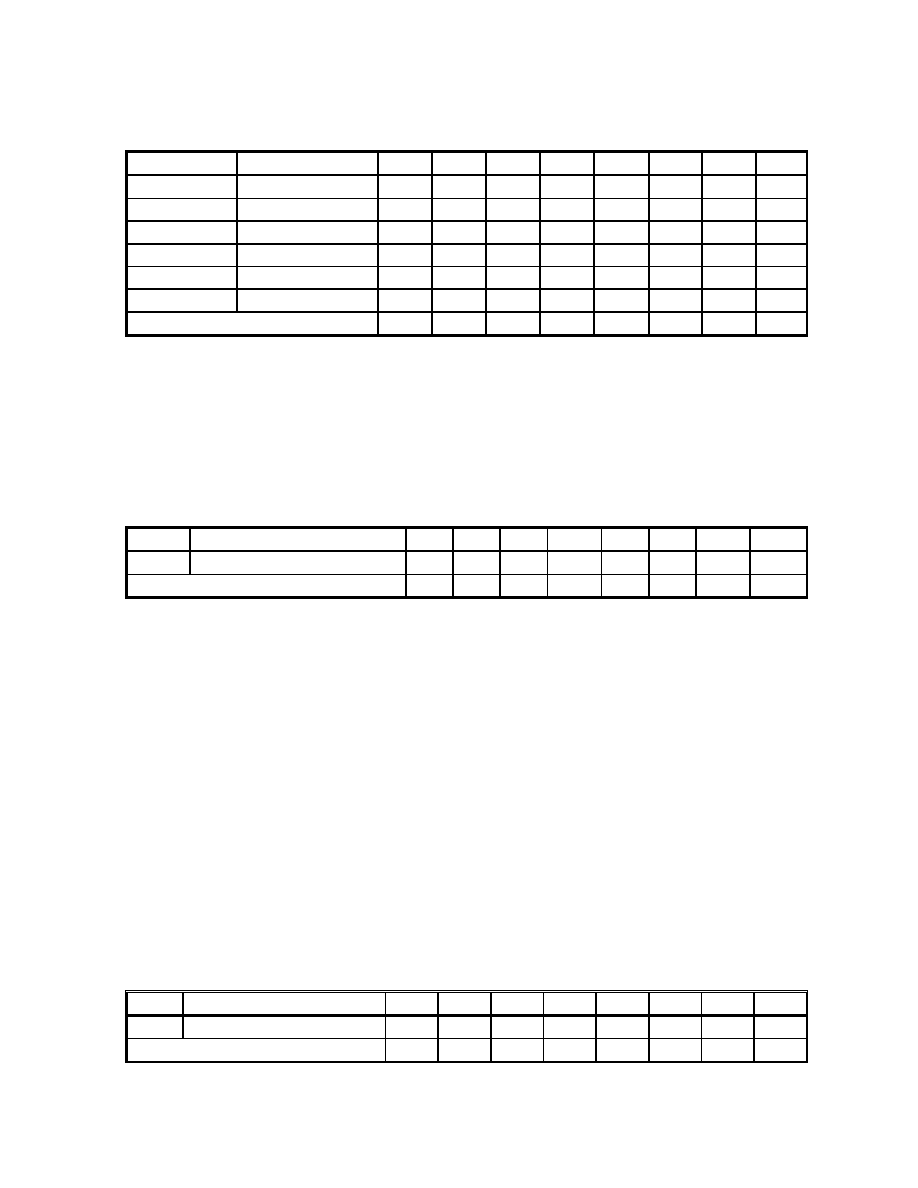
A Droop correction filter is included in the TCD6001 to correct for droop and ripple in the frequency response
of the entire signal processing chain. The frequency response of the droop filter for the 1X, 2X, and 4X
sampling modes is shown below.
Figure 3. Frequency response of the Droop Correction Filter
Sampling Rate Control
Addr
Register
Name
D7 D6 D5 D4 D3 D2 D1 D0
22h
Sampling Rate Control
0
0
0
1Xf 1Xs 0
S4X S2X
Default
0
0
0
0 0 0
0 0
This register allows the user to specify the data-sampling rate (1X, 2X or 4X). When the 1X mode is selected
and the de-emphasis filter is enabled, 1Xf and 1Xs select between 32 kHz, 44.1kHz, and 48 kHz de-
emphasis filters.
Bits S4X S2X
0
0
1X mode (32 kHz, 44.1 kHz, or 48 kHz)
0
1
2X mode (96 kHz)
1
0 or 1
4X mode (192 kHz)
Bits 1Xf 1Xs
0
0
data-sampling rate is 44.1 kHz
0
1
data-sampling rate is 32 kHz
1
0
data-sampling rate is 48 kHz
1 1 not
used
If the 2X or the 4X modes are selected, the de-emphasis filter is automatically disabled, and the setting of bit
D6 in the Filter Bypass Control register (address 21h) will be ignored.
Operation Control
Addr
Register
Name
D7 D6 D5 D4 D3 D2 D1 D0
23h Operation
Control 0
1
0
0
HFR
0
R1 R0
Default
0
1
0
0
0
0
1 1
This register allows the user to specify 2 operational characteristics of the TCD6001:
0
2
4
6
8
10
x 10
4
-0.5
-0.4
-0.3
-0.2
-0.1
0
0.1
0.2
0.3
0.4
0.5
Frequency in kHz
db
Total Effective D roop, After Correction
1x mode
2x mode
4x mode

Tripath Technology, Inc. ≠ Preliminary Technical Information
22
TCD6001 ≠ JL/Rev. 0.9/07.05
-
The Sync Reset mode (control bits R0 and R1)
-
The High Frequency Master Clock option (control bit HFR)
If the Left/Right channel clock (LRCK) and Bit clock (BITCK) are not properly synchronized with the Master
clock (MCK) and R0 is set to `1', a "Sync Reset" is generated. If R1 is also set to `1' a hard mute is issued
during the Sync Reset and released after the Sync Reset is released.
During a Sync Reset the DATAnn inputs are ignored and digital silence is substituted. The TCD6001 waits
for the clocks to be synchronized before coming out of reset. During Sync Reset, the internal automatic DC
offset calibration values are cleared. When the clocks are restored, the system will need to be re-calibrated
by hard muting and un-muting or by forcing a DC calibration value in the Calibration Bank.
The Sync Reset is different from an external reset, which is created by pulling the RESETB pin low. A Sync
Reset will not change the values of I2C addressable read/write registers.
R1 enables a "Hard-mute" upon Sync Reset. When the Sync Reset condition is removed, an auto-calibration
will take place before the outputs are restored. R0 must be set to `1' for R1 to have any effect.
The Master Clock (MCK) input frequency is determined by a combination of the S4X, S2X, and HFR bits and
the sampling frequency. The phase of MCK is not critical, as long as the frequency is correctly set. When the
HFR bit (register 23h, bit D3) is set to `1', the TCD6001 divides MCK by 2 so that higher frequency system
clocks may be used. The duty cycle of MCK should be between 48% and 52% unless HFR is set to `1'. In
this case, the division automatically creates a 50% duty cycle internal clock.
HFR S4X
S2X
MCK pulses
per sample
0 0
0
256
0 0
1
128
0 1
0
64
0 1
1
64
1 0
0
512
1 0
1
256
1 1
0
128
1 1
1
128
The following table shows some examples of the MCK clock frequency based on sampling rate and HFR:
Data sampling rate
32 kHz
44.1 kHz
48 kHz
96 kHz
192 kHz
MCK frequency (HFR = `0')
8.192 MHz
11.289 MHz
12.288 MHz
12.288 MHz
12.288 MHz
MCK frequency (HFR = `1')
16.384 MHz
22.578 MHz
24.576 MHz
24.576 MHz
24.576 MHz
Digital Input Format
Addr
Register
Name
D7 D6 D5 D4 D3 D2 D1 D0
24h
Digital Input Format
0
DP BCK CCK I2S LRA DW1 DW0
Default
0
0 1 0 0 0 1 1
This register allows the user to specify the following digital interface characteristics:
-
Input data width (DW0 and DW1)
-
Input data alignment with respect to LRCK clock edges (LRA)
-
Polarity of the LRCK clock (CCK)
-
Polarity of the BITCK clock (BCK)
-
Polarity of the input data (DP)
The TCD6001 receives PCM digital audio data in I2S format or variations thereof. The format consists of an
audio data input (DATAnn), a bit clock (BITCK) that runs at 64x the sampling frequency, and a 1x sampling

Tripath Technology, Inc. ≠ Preliminary Technical Information
23
TCD6001 ≠ JL/Rev. 0.9/07.05
frequency clock (LRCK). In addition, a master clock (MCK) synchronizes all digital operations inside the
device. Each DATAnn input carries serial data for 2 channels. The LRCK clock differentiates between odd
and even channel data. BITCK is synchronized with the serial data input, and latches data on either rising
edges or falling edges of BITCK (programmable option).
The TCD6001 has 3 serial data inputs (DATA12, DATA34, and DATA56) and therefore can receive 6
channels of audio data. The group of bits received on a DATAnn input during a half period of LRCK clock is
called a PCM data sample. It is a 2's complement representation of the amplitude of sound on that channel
at that time.
There are 32 pulses of BITCK for every half period of LRCK. So, in theory, it is possible to read up to 32 bits
of data per sample. However, only a maximum of 24 bits are read. The device will also accept 16, 18, and
20 bit formats depending on what has been specified in the control registers.
The most significant bit of data always arrives first and the least significant bit last. Data can be left aligned
or right aligned to the LRCK clock. If data is left aligned, the most significant bit of data arrives at the
beginning of the LRCK half-period. If data is right aligned, the least significant bit of data arrives just before
the end of the LRCK half-period.
DW1 and DW0 define the input data width. Any data outside of the selected data width will be ignored.
DW1
DW0
Input Data Width
0 0
16
bit
0 1
18
bit
1 0
20
bit
1 1
24
bit
LRA specifies the left/right data alignment scheme. When LRA is `0', data is left aligned to LRCK transitions.
When LRA is `1', data is right aligned to LRCK transitions.
If data is left aligned, the most significant bit of data can arrive on the first or the second BITCK pulse. The
I2S format specifies that it arrive on the second BITCK pulse. When the I2S control bit is `1', the data
conforms to the I2S standard - the most significant data bit is read during the second BITCK pulse. When
the I2S control bit is `0', the most significant data bit is read during the first BITCK pulse. If data is right
aligned, the I2S control bit has no effect.
When CCK is `0', even channel data (channels 2, 4, and 6) is read while LRCK is high and odd channel data
(channels 1, 3, and 5) is read while LRCK is low. When CCK is `1', odd channel data is read while LRCK is
high and even channel data is read while LRCK is low.
When BCK is `1', data is latched on the falling edge of BITCK. When BCK is `0', data is latched on the rising
edge of BITCK.
DP is used to specify the polarity of the 2's complement audio data. If DP is `0', the data is non-inverted. If
DP is `1', the data is inverted.
Figure 1 shows several examples of digital input format. Notice that for a given stereo audio sample, the
TCD6001 reads even channels first and then the odd channels. I2S and most of its variations first send left
channel data and then right channel data within stereo audio sample frames. Therefore, the TCD6001 sends
left channel input data to output channels 2, 4 and 6 and right channel input data to output channels 1, 3,
and 5.
Inverting CCK to send left channel data to odd channels can potentially cause phase shift problems. For
example, if standard I2S data is received with register 24h = 0Bh instead of 1Bh, stereo data frames are
read beginning with the rising edge of LRCK instead of the falling edge. This means that left and right
channel data will be out of phase by Ω of a LRCK cycle.

Tripath Technology, Inc. ≠ Preliminary Technical Information
24
TCD6001 ≠ JL/Rev. 0.9/07.05
MSB
LSB
MSB
LSB
ch 2, 4, 6
ch 1, 3, 5
ch 2, 4, 6
ch 1, 3, 5
LRCK
BITCK
DATAnn
LRCK
BITCK
DATAnn
DW
0
DW
1
LR
A
I2S
CCK
BC
K
REG 24h
1
1
0
0
0
0
0
0
DP
TE
S
T
1
1
0
1
1
0
0
0
ch 2, 4, 6
ch 1, 3, 5
LRCK
BITCK
DATAnn
LRCK
BITCK
DATAnn
1
1
0
0
1
0
0
0
1
1
0
1
0
0
0
0
ch 2, 4, 6
ch 1, 3, 5
MSB
LSB
ch 2, 4, 6
ch 1, 3, 5
LRCK
BITCK
DATAnn
0
0
1
0
0
0
0
0
MSB
LSB
LSB
16
Bits
16
Bits
STEREO AUDIO SAMPLE
MSB
LSB
ch 2, 4, 6
ch 1, 3, 5
LRCK
BITCK
DATAnn
1
0
1
0
0
0
0
0
MSB
LSB
LSB
18
Bits
18
Bits
MSB
LSB
ch 2, 4, 6
ch 1, 3, 5
LRCK
BITCK
DATAnn
0
1
1
0
0
0
0
0
MSB
LSB
LSB
20
Bits
20
Bits
MSB
LSB
ch 2, 4, 6
ch 1, 3, 5
LRCK
BITCK
DATAnn
1
1
1
0
0
0
0
0
MSB
LSB
LSB
24
Bits
24
Bits
24
Bits
MSB
LSB
24
Bits
8
Bits
8
Bits
MSB
LSB
24
Bits
MSB
LSB
24
Bits
8
Bits
8
Bits
24
Bits
7
Bits
MSB
LSB
24
Bits
7
Bits
MSB
LSB
24
Bits
7
Bits
MSB
LSB
24
Bits
7
Bits
16
Bits
16
Bits
14
Bits
14
Bits
12
Bits
12
Bits
8
Bits
8
Bits
Figure 1 Digital Audio Input Formats
Tripath Technology, Inc. ≠ Preliminary Technical Information
25
TCD6001 ≠ JL/Rev. 0.9/07.05
Channel Volume
Addr
Register
Name D7 D6 D5 D4 D3 D2 D1 D0
25h
Channel
1
Volume V17 V16 V15 V14 V13 V12 V11 V10
26h
Channel
2
Volume V27 V26 V25 V24 V23 V22 V21 V20
27h
Channel
3
Volume V37 V36 V35 V34 V33 V32 V31 V30
28h
Channel
4
Volume V47 V46 V45 V44 V43 V42 V41 V40
29h
Channel
HP1
Volume VH17 VH16 VH15 VH14 VH13 VH12 VH11 VH10
2Ah
Channel
HP2
Volume VH27 VH26 VH25 VH24 VH23 VH22 VH21 VH20
Default
0 0 0 0 0 0 0 0
The TCD6001 has 6 channel volume registers, one for each channel. The 8-bit value in each register
represents the volume loudness for the corresponding channel. The least significant bit, D0, represents a
volume increment of 0.5dB. Therefore the total range available is 128dB. Maximum volume is achieved
when the volume register contains a value of FFh, and no sound is heard if its value is 00h.
In addition, a "coarse gain" adjustment (1X, 2X, 4X, and 8X) is made possible by programming the Volume
Change Control Register.
Volume Ramp Rate
Addr
Register
Name
D7 D6 D5 D4 D3 D2 D1 D0
2Bh
Volume
Ramp
Rate
RR7 RR6 RR5 RR4 RR3 RR2 RR1 RR0
Default
1 0 0 0 0 0 0 0
The TCD6001 can be programmed to have volume changes take effect immediately or be ramped at a
predefined rate for all channels. If the Volume Ramp Enable bit is set, the Volume Ramp Rate Register
defines the ramp rate.
Although the Volume Control Registers define the channel volume within an accuracy of Ω dB, volume will
be ramped internally in 1/8 dB steps when ramping is enabled.
The number entered into the Volume Ramp Rate Register can be from 0 (00h) to 255 (FFh). If the number
entered is N, the time delay between two consecutive 1/8 dB volume increments is equal to:
N x (4 periods of LRCK)
As an example, if N = 100 and data samples are coming in at a 44.1kHz rate, the period of LRCK is
22.67usec. The delay between two consecutive 1/8 dB volume increments is:
100 x 4 x 22.67usec = 9068usec
Therefore if the volume change is 60 dB (480 increments of 1/8 dB), the total ramp time will be:
480 x 9068usec = 4.32 second
Channel Mute Control
Addr
Register
Name
D7 D6 D5 D4 D3 D2 D1 D0
2Ch
Channel Mute Control
MH2
MH1
M4
M3
M2
M1
HM
AM
Default
0 0 0 0 0 0 1 0
The TCD6001 has 3 different Mute functions: Soft-Mute, Hard-Mute, and Auto-Mute.

Tripath Technology, Inc. ≠ Preliminary Technical Information
26
TCD6001 ≠ JL/Rev. 0.9/07.05
The Soft-Mute function will turn off volume selectively on any of the 6 channels. Setting control bits M1
through MH2 to `1' will issue a Soft-Mute on the corresponding channels. If the VRE bit in the Volume
Change Control Register is set, the volume will first ramp down at a rate defined by the Volume Ramp Rate
Register. Soft-Mute has no affect on whether the differential outputs (Y1 and Y1B through Y4 and Y4B)
continue to switch or not. Clearing bits M1 through MH2 to `0' will re-establish volume on all channels at a
rate defined by the Volume Ramp Enable settings.
The Hard-Mute function is enabled by setting control bit HM high. This function starts with a Soft-Mute on all
channels simultaneously. If the VRE bit in the Volume Change Control Register is set, the volume will first
ramp down at a rate defined by the Volume Ramp Rate Register. Once volume is turned off on all channels,
all differential outputs (Y1 and Y1B through Y4 and Y4B) stop switching. This will reduce power consumption
in the power stages driven by the TCD6001.
When control bit HM is cleared to `0', the Hard-Mute condition is removed, and the TCD6001 goes through
an automatic DC calibration cycle. Once the calibration cycle is complete, volume is re-established on all
channels at a rate defined by the Volume Ramp Enable settings.
The Auto-Mute function is enabled by setting the AM bit to `1'. This function detects digital silence (all data
input bits at 0) on all 6 channels lasting more than a pre-defined delay. It then issues a Hard-Mute. The
delay is determined by the contents of the Auto-Mute Timing Register (described below). Upon arrival of
non-zero data on any channel, the Hard-Mute condition is automatically removed. The volume on all 6
channels is re-established at a rate defined by the Volume Ramp Enable settings. The Auto-Mute function
reduces power consumption in the power stages during periods of silence.
Auto-Mute Timing
Addr
Register
Name
D7 D6 D5 D4 D3 D2 D1 D0
2Dh
Auto-Mute
Timing
AM7 AM6 AM5 AM4 AM3 AM2 AM1 AM0
Default
0 0 0 0 0 0 0 0
This register is only used if the Auto-Mute function is enabled. Its contents specify the duration of silence on
all 6 channels before a Hard-Mute condition is issued. If the number entered is "N", the duration of silence is
equal to:
(2N + 1) x (1,048,576 periods of LRCK)
As an example, if N = 1 and the period of LRCK is 22.67usec, the period of silence required before a Hard-
Mute condition is issued is:
3 x 1,048,576 x 22.67usec = 71.3 seconds
Volume Change Control
Addr
Register
Name
D7 D6 D5 D4 D3 D2 D1 D0
2Eh Volume
Change
Control 0
0
0
0
VR1 VR0 VRE ZCE
Default
0
0
0
0
0 1 0 0
This register is used to specify 3 characteristics of volume change for all channels:
-
Coarse Gain (control bits VR0 and VR1)
-
Volume Ramp Enable (control bit VRE)
-
Zero-Crossing Enable (control bit ZCE)
Coarse Gain is a simple volume adjustment made by shifting bits to the left. Coarse Gain is set by selecting
one of four combinations for bits VR0 and VR1. Coarse Gain affects all 6 channels globally.
Coarse Gain can cause premature digital clipping when used with PGC because internal digital gain
approaches maximum at each PGC boundary. Therefore when using PGC, Coarse Gain should not be
enabled until maximum volume has been reached on all channels.

Tripath Technology, Inc. ≠ Preliminary Technical Information
27
TCD6001 ≠ JL/Rev. 0.9/07.05
Bits VR1 VR0
0 0 1X
volume
0 1 2X
volume
1 0 4X
volume
1 1 8X
volume
The VRE control bit is the Volume Ramp Enable bit. If VRE = `1', the contents of the Volume Ramp Rate
Register will be read and determine how fast the volume can ramp up or down on all 6 channels. Refer to
the Volume Ramp Rate Register section for a more detailed explanation of how the ramp rate is calculated.
The ZCE control bit is the Zero-Crossing Enable bit. A polarity inversion on the audio input signal is called a
"Zero-Crossing". Changing volume only at Zero-Crossings helps to avoid popping sounds. If ZCE is set to
`1', volume will only be allowed to change at Zero-Crossings. However, if a Zero-Crossing does not occur
within a time defined by the Volume Ramp Rate Register (called "time-out" in the graph below), volume will
change anyway. If the Zero-Crossing feature is enabled, the VRE control bit will still control whether the
volume change occurs in one large step or in 1/8 dB steps at Zero-Crossings.
No zero-crossing, volume change
occurs after time-out
Volume change occurs at every
zero-crossing
Audio signal
Time
Amplitude
time-out

Tripath Technology, Inc. ≠ Preliminary Technical Information
28
TCD6001 ≠ JL/Rev. 0.9/07.05
Volume Change Flowchart
Volume change
requested
VRE = 1
?
Wait for timeout
ZCE = 1
?
Wait for zero
crossing or
timeout (whichever
comes first)
Change volume
by 1/8 dB
Reached
desired
setting?
End
Wait for timeout
ZCE = 1
?
Wait for zero
crossing or
timeout (whichever
comes first)
Change volume to
desired setting
End
No
Yes
No
Yes
Yes
No
No
Yes

Tripath Technology, Inc. ≠ Preliminary Technical Information
29
TCD6001 ≠ JL/Rev. 0.9/07.05
Automatic DC Offset Calibration Control
Addr
Register
Name
D7 D6 D5 D4 D3 D2 D1 D0
2Fh
Automatic DC Calibration Control
0
CAB CFH2
CFH1 CF4 CF3 CF2 CF1
Default
0
0 0 0 0 0 0 0
The CFn bits control which DC offset calibration values will be used. If a particular channel's CFn bit is set to
`1', the value stored in the Calibration Bank registers will be used. If CFn is cleared to `0', the Automatic DC
Offset Calibration values that were calculated after coming out of hard mute will be used.
Setting the CAB bit to `1' will bypass Automatic DC Offset Calibration. DCX works in conjunction with the
CAB bit. DCX should be set to the same value as CAB.
For normal operation, CFH1 and CFH2 should be set to `1'.
Calibration Bank
Addr
Register
Name
D7 D6 D5 D4 D3 D2 D1 D0
30h
Calibration
Bank
CB19 CB18 CB17 CB16 CB15 CB14 CB13 CR12
31h
Calibration
Bank
CB29 CB28 CB27 CB26 CB25 CB24 CB23 CR22
32h
Calibration
Bank
CB39 CB38 CB37 CB36 CB35 CB34 CB33 CR32
33h Calibration
Bank 0
0
CB31 CB30 CB21 CB20 CB11 CR10
34h
Calibration
Bank
CB49 CB48 CB47 CB46 CB45 CB44 CB43 CR42
35h
Calibration
Bank
CH19 CH18 CH17 CH16 CH15 CH14 CH13 CH12
36h
Calibration
Bank
CH29 CH28 CH27 CH26 CH25 CH24 CH23 CH22
37h Calibration
Bank 0
0
CH21 CH20 CH11 CH10 CB41 CR40
Default
0 0 0 0 0 0 0 0
These registers store calibration values that can be forced instead of the automatic DC calibration values.
Register 2Fh controls whether the automatic values will be used or the Calibration Bank values. The DC
calibration values are 10 bit words so they are stored in separate bytes. For example, for channel 1, the 8
most significant bits are stored in register 30h, while the 2 least significant bits are stored in register 05h ≠
bits D1 and D0.
For normal operation, all CH1n and CH2n bits should be cleared to `0'.
Force DC
Addr
Register
Name
D7 D6 D5 D4 D3 D2 D1 D0
38h
Force
DC
FD7 FD6 FD5 FD4 FD3 FD2 FD1 FD0
Default
0 0 0 1 1 1 0 0
This register is used to force a DC offset in the system. It is used for testing purposes. It should be changed
from its default setting to 00h for normal operation.

Tripath Technology, Inc. ≠ Preliminary Technical Information
30
TCD6001 ≠ JL/Rev. 0.9/07.05
Dither Control
Addr
Register
Name
D7 D6 D5 D4 D3 D2 D1 D0
39h
Dither
Control
DT7 DT6 DT5 DT4 DT3 DT2 DT1 DT0
Default
0 0 0 0 0 0 0 0
This register is used to set the amount of dither in the system. It should be set to 3Ch for normal operation.
Fault Latch Control
Addr
Register
Name
D7 D6 D5 D4 D3 D2 D1 D0
3Ah
Fault Latch Control
0
0
0
0
0
FLD FLC 0
Default
0
0
0
0
0
1 0 0
FLD and FLC control the TCD6001 behavior after FAULT has been asserted.
If FLD is set to `1', the TCD6001 will automatically un-mute after FAULT is released (floated).
If FLD is cleared to `0', the TCD6001 will remain latched in this FAULT-based muted condition until the
FAULT pin is released and FLC undergoes a `0' to `1' transition.
Saturation Clamp
Addr
Register
Name
D7 D6 D5 D4 D3 D2 D1 D0
3Bh
Saturation Clamp LSB
1
1
1
1
1
1
1
1
3Ch
Saturation Clamp MSB
1
1
1
0
0
1
1
1
The Saturation Clamp is a 16 bit word that determines the internal digital saturation point. It should be set to
E7FFh for the maximum range of operation.
Predictive Gain Control
Addr
Register
Name
D7 D6 D5 D4 D3 D2 D1 D0
3Dh
Predictive Gain Control
PGC
0
0
0
0
0
0
0
Default 0
0
0
0
0
0
0
0
Predictive Gain Control is enabled when PGC is set to `1'. It is disabled when PGC is cleared to `0'. PGC
should not be turned on or off while not in hard-mute. Doing so will have unpredictable results.
Output Delay Control
Addr
Register
Name
D7 D6 D5 D4 D3 D2 D1 D0
71h
Output
Delay
Control
YD23 YD22 YD21 YD20 YD13 YD12 YD11 YD10
72h
Output
Delay
Control
YD43 YD42 YD41 YD40 YD33 YD32 YD31 YD30
Default
0 0 0 0 0 0 0 0
The loop delay of each channel can be selectively increased by programming its corresponding 4-bit field.
Adjusting loop delay can be used to control power stage switching frequency. Switching frequencies should
be staggered by at least 40kHz to avoid beat frequencies that can increase the noise floor.

Tripath Technology, Inc. ≠ Preliminary Technical Information
31
TCD6001 ≠ JL/Rev. 0.9/07.05
YD<3:0>
Actual count
Processor Y-output delay
0000 1
15
nS
0001 2
30
nS
0010 3
45
nS
0011 4
60
nS
0100 5
75
nS
0101 6
90
nS
0110 7
105
nS
0111 8
120
nS
1000 9
135
nS
1001 10
150
nS
1010 11
165
nS
1011 12
180
nS
1100 13
195
nS
1101 14
210
nS
1110 15
225
nS
1111 16
240
nS
Truth table for Y-output delay control.
Startup Burst Control
Addr
Register
Name
D7 D6 D5 D4 D3 D2 D1 D0
73h
Startup Burst Control
0
0
0
0
0
0
STB1 STB0
Default
0
0
0
0
0
0
0 0
The STBn control bits enable startup bursts for driving bootstrapped output stages such as the TP2150B
and TP2350. When using power stages that do not require startup bursts, STB1 and STB0 should be
cleared to 0 to minimize turn-on pops.
STB<1:0>
Number of startup pulses
00 0
01 4
10 8
11 16
.
Headphone and Logic Output Control
Addr
Register
Name
D7 D6 D5 D4 D3 D2 D1 D0
74h
Headphone and Logic Output
0
YSN HPO TO
0
0
0
0
Default
0
0 0 0 0
0
0
0
Setting the TO control bit to `1' forces the TST_EN output pin to go high. This pin can be used to put the
power stage IC into test mode. If the power stage does not have a TST_EN input, the TST_EN output can
be used as a general purpose logic output.
Setting HPO to `1' immediately stops all switching without muting the headphone amplifier outputs. This
function can be used to mute all power stage outputs while the user listens to the headphone output. If any
of the power stages being used only have single Yn inputs (like the TPD2075 and TPD2125) instead of Y/Yb
combinations, HMF should be used instead. HPO should be cleared to '0' for normal operation.

Tripath Technology, Inc. ≠ Preliminary Technical Information
32
TCD6001 ≠ JL/Rev. 0.9/07.05
The YSN control bit is internally XORed with the SE/BRGB pin to determine the timing of the HMUTE and
Yn/YnB outputs after automatic DC calibration. Normally, after automatic DC calibration, Yn and YnB are
held low while HMUTE is de-asserted. Then, channels begin switching one by one until all are switching.
This can help reduce startup current requirements. However, if the power stage that is being used is single
ended and has no YnB inputs because it generates its own YnB signal internally, the staggered turn-on
timing will cause the power stage outputs to be held to the negative power supply until switching begins.
This will result in a loud pop and possible speaker damage. Therefore, in this case, YSN and SE/BRGB
should be configured for immediate turn-on.
YSN SE/BRGB
Turn-On
Timing
0 0
Staggered
0 1
Immediate
1 0
Immediate
1 1
Staggered
Output Timing Control
Addr
Register
Name
D7 D6 D5 D4 D3 D2 D1 D0
76h Output
Timing
Control DEL
DCB
DCX
0
HMF BB2 BB1 BB0
Default 1
ext
ext
0
0 0 0 0
Control bits BB0 through BB2 are used to program a "break before make" delay in the Y outputs.
Break before make is a dead time at the Y-outputs where both Y and YB of each channel are low together
for a period of time in order to prevent shoot-through current in the output power MOSFET devices.
.
BB<2:0> BBM
Delay
000 0
nS
001 15
nS
010 30
nS
011 45
nS
100 60
nS
101 75
nS
110 90
nS
111 105
nS
Break before make (BBM) delay table
Some Tripath power stages like the TPS4070, the TPS4100, the TPD2075, and the TPD2125 handle BBM
themselves. For these and any other power stages that handle BBM on their own, TCD6001 BBM should be
set to 0 nS.
The HMF control bit, when set to `1', forces the HMUTE output high regardless of the state of the system.
HMUTE operates normally when HMF is cleared to `0'. This function can be used to mute all power stage
outputs while the user listens to the headphone output. During automatic DC calibration the TCD6001
expects to be able to turn off both the high and low side FETs by pulling Y and Yb low. However, some
power stages like the Tripath TPD2075 and TPD2125 only have a single Y input instead of complimentary Y
and Yb inputs. When using this type of power stage, during automatic DC calibration, HMF should be set to
`1'. This keeps the HMUTE output high during automatic DC calibration. After waiting for automatic DC
calibration to complete, HMF can be cleared to `0' to resume normal switching. When using other power
stages, HMF should be kept at `0'.

Tripath Technology, Inc. ≠ Preliminary Technical Information
33
TCD6001 ≠ JL/Rev. 0.9/07.05
When DCX is set to `1', automatic DC calibration is disabled. The default value of DCX is set by the
BYP_CAL input. When BYP_CAL = 5V, DCX will be `1' at power-on. When BYP_CAL = GND, DCX will be
`0' at power-on. DCX works in conjunction with the CAB bit. DCX should be set to the same value as CAB.
DCB controls the method of automatic DC calibration that will be used. DCB should be set to `1' if a bridged
output stage is being used. DCB should be cleared to `0' if a single ended output stage is being used. The
BCn bits work in conjunction with the DCB bit. When DCB is set to '1', the BCn bits that correspond to the
channels that have bridged output stages connected to them should be set to '1'. When DCB is cleared to
'0', all of the BCn bits should be cleared to '0'. The default value of DCB will be the inversion of the
SE/BRGB pin. When SE/BRGB = GND, DCB will be '1' at power-on. When SE/BRGB = 5V, DCB will be '0'
at power-on.
The DEL control bit enables the on-chip delay compensation. Delay compensation corrects for loop
instability that can be caused by propagation delay through power stages. It should always be set to `1'.
Individual Hard Mute Control
Addr
Register
Name
D7 D6 D5 D4 D3 D2 D1 D0
77h
Individual Hard Mute Control
0
HM4 HM3 HM2 HM1 0
0
0
Default
0
0 0 0 0 0
0
0
Setting an HMn bit to `1' stops switching on an individual output channel. Clearing the bit to `0' resumes
normal operation.
Post-Gain Control
Addr
Register
Name
D7 D6 D5 D4 D3 D2 D1 D0
7Ah
Post
Gain
Control
GN41 GN40 GN31 GN30 GN21 GN20 GN11 GN10
Default ext
ext
ext
ext ext ext ext ext
Post-gain adjusts the maximum output level with respect to the power stage supply voltage. Post gain
settings `00' and `01' decrease the noise floor while limiting output power. Post gain setting `11' allows a
signal to be severely clipped for maximum power measurements.
GNn<1:0> Post-gain
00 -6.5
dB
01 -3.5
dB
10 0
dB
11 +2.5
dB
OV and SLEEPB control
Addr
Register
Name
D7 D6 D5 D4 D3 D2 D1 D0
7Ch
OV and SLEEPB Control
0
0
SLPB OVDB 0
0
0
0
Default
0
0
1 1 0
0
0
0
Clearing the OVDB control bit to `0' disables the over voltage sense circuit. Setting the OVDB control bit to
`1' returns the over voltage sense circuit to normal operation. The under voltage sense circuit functions
normally regardless of the state of OVDB.
The SLPB control bit determines the state of the SLEEPB_OUT pin. When SLPB is set to '0', SLEEP_OUT
is 0V. When SLPB is set to '1', SLEEP_OUT is 5V. This pin can be used to put the power stage IC into sleep
mode. The SLPB control bit has no internal affect on the TCD6001. If the power stage does not have a
SLEEPB input, the SLEEPB_OUT output can be used as a general purpose logic output.

Tripath Technology, Inc. ≠ Preliminary Technical Information
34
TCD6001 ≠ JL/Rev. 0.9/07.05
B-Cal control
Addr
Register
Name
D7 D6 D5 D4 D3 D2 D1 D0
7Dh
B Cal Control
0
0
0
BC4 BC3 BC2 BC1 0
Default
0
0
0
0 0 0 0 0
The BCn control bits control the method of automatic DC calibration that will be used for individual channels.
BCn should be set to `1' if a bridged output stage is being used. BCn should be cleared to `0' if a single
ended output stage is being used. The BCn bits work in conjunction with the DCB bit. When DCB is set to
'1', the BCn bits that correspond to the channels that have bridged output stages connected to them should
be set to '1'. When DCB is cleared to '0', all of the BCn bits should be cleared to '0'.

Tripath Technology, Inc. ≠ Preliminary Technical Information
35
TCD6001 ≠ JL/Rev. 0.9/07.05
I2C Programming Examples
Initialization string for a bridged output stage with its own BBM:
sub-address value
20h
00000000b
Un-freeze registers. System starts in mute so the instruction sequence is not
important.
21h
11000000b
Turn off de-emphasis and DC blocking filters. Turn on droop correction filter.
22h
00010000b
48kHz sampling rate.
23h
01000011b
MCK will be 48kHz * 256 = 12.288MHz. Sync Reset is on and it will trigger a
hard-mute.
24h
00011011b
Standard I2S format.
25h
00h
Channel 1 Volume
26h
00h
Channel 2 Volume
27h
00h
Channel 3 Volume
28h
00h
Channel 4 Volume
29h 00h Channel
HP1
Volume
2Ah 00h Channel
HP2
Volume
2Bh
00h
Leave Volume Ramp Rate at 00h while not changing volume.
2Ch
00000010b
Start out in hard-mute. Turn off Auto-Mute.
2Dh 00h Auto-Mute
Timing
2Eh
00000011b
Coarse Gain = 1x. Volume Ramp Enable and Zero Crossing Enable
2Fh
01100000b
Bypass DC calibration for headphone outputs.
30h 00h CalibBank0Ex
31h 00h CalibBank1Ex
32h 00h CalibBank2Ex
33h 00h CalibBank012Ex
34h 00h CalibBank3Ex
35h 00h CalibBank4Ex
36h 00h CalibBank5Ex
37h 00h CalibBank345Ex
38h
00h
Clear Force DC register.
39h
3Ch
Set Dither Control to 3Ch.
3Ah
00000100b
Enable Fault Latch.
3Bh
FFh
Always set Saturation Clamp to these values.
3Ch
E7h
Always set Saturation Clamp to these values.
3Dh
10000000b
Turn on PGC.
71h
10111010b
Stagger switching frequencies.
72h
11011100b
Stagger switching frequencies.
73h
00000000b
Turn of Startup Burst if not needed.
74h
00000000b
YSN = 0, HPO = 0, TST_EN output is low.
75h 00h Test.
76h
10000110b
Enable Delay compensation. Use B-cal for bridged output. Enable automatic
DC calibration. Normal HMUTE operation. No BBM.
77h
00000000b
Individual channel hard mutes are inactive.
78h 00h Test.
79h 00h Test.
7Ah
01010101b
Set Post-Gain for all channels to 0dB.
7Bh 00h Test.
7Ch
00110000b
Normal OV/UV operation. SLEEP_OUT = high.
7Dh
00011110b
All channels use B-cal for bridged output.
To Un-mute a bridged output stage:
sub-address value
77h
01111000b
Prevent switching until after automatic DC calibration is complete.
2Ch
00000000b
Remove Hard-Mute to begin automatic DC calibration.
<If PGC is on, wait 4 seconds for automatic DC calibration. If PGC is off, wait 1 second for calibration.>
77h 00000000b
Begin
switching.

Tripath Technology, Inc. ≠ Preliminary Technical Information
36
TCD6001 ≠ JL/Rev. 0.9/07.05
To change the volume:
sub-address value
2Bh
01h
Set Volume Ramp Rate to a nonzero value to prevent pops.
26h
xxh
Set volume levels.
27h
xxh
Set volume levels.
28h
xxh
Set volume levels.
29h
xxh
Set volume levels.
2Ah xxh Set
volume levels.
2Bh
00h
Clear Volume Ramp Rate to force volume in case zero crossings have not
occurred.
When increasing or decreasing the volume past a PGC boundary (when PGC is enabled), extra care
must be taken to avoid pops. When crossing a PGC boundary, make sure that the boundary is being
crossed by at least two volume steps. See the following two examples:
When increasing the volume past a PGC boundary (for example - from F3h to F4h)
sub-address value
2Bh
01h
Set Volume Ramp Rate to a nonzero value to prevent pops
2Ch
F3h
Volume starts at F3h. PGC boundary is between F3h (1/2 PGC) and F4h (full
PGC).
2Ch
F2h
Instead of changing the volume directly from F3h to F4h, first increase the
volume by 1.
2Ch
F4h
Then set the volume to F4h to allow an additional ramp for avoiding pops.
2Bh
00h
Clear Volume Ramp Rate to force volume in case zero crossings have not
occurred.
When decreasing the volume past a PGC boundary (for example - from DCh to DBh)
sub-address value
2Bh
01h
Set Volume Ramp Rate to a nonzero value to prevent pops
2Ch
DCh
Volume starts at DCh. PGC boundary is between DCh (1/4 PGC) and DBh
(1/8 PGC).
2Ch
DDh
Instead of changing the volume directly from DCh to DBh, first increase the
volume by 1.
2Ch
DBh
Then set the volume to DBh to allow an additional ramp for avoiding pops.
2Bh
00h
Clear Volume Ramp Rate to force volume in case zero crossings have not
occurred.

Tripath Technology, Inc. ≠ Preliminary Technical Information
37
TCD6001 ≠ JL/Rev. 0.9/07.05
Output Characteristics
The TCD6001 outputs consist of four pairs of complementary 1-bit digital data streams, one pair per audio
channel as well as stereo line-out / head phone amplifier. The complementary 1-bit digital streams switch
from 0V to 5V (+/- 10%) and constitute a pulse-density-modulated (PDM) form of the audio signal. They are
used to drive Tripath power stages in a switching amplifier configuration. The head phone amplifier is
capable of driving XXmW into 32 ohm loads.
The output power of a power stage can be expressed as V
2
/R, V being the voltage amplitude of the power
stage output and R the speaker input impedance, typically 4 to 8 ohms.
The audio signal is recovered by filtering the PDM signal through an LC filter located at the inputs of the
speaker. The following figure shows the power stage output waveform and the filtered signal at the speaker
inputs:
Typical waveform at power stage output
Typical waveform at speaker inputs after LC filtering
TCD6001 outputs are pulse density modulated outputs. Their frequency varies constantly over time and can
typically reach a maximum value of 800 kHz.
A Mute output (HMUTE) can be connected to all 4 power stages to force them into a tri-state mode when a
hard mute condition is encountered. The HMUTE output can be programmed to be either active-high or
active-low via the pin HMUTE_SET. The HMUTE_SET input range is 0 to 5V with 3.3V compliant inputs.
Setting HMUTE_SET will result in HUMTE being low during a fault condition. Setting HMUTE_SET high will
result in HMUTE being high during a fault condition.
An overload is detected whenever the combination of input signal amplitude and volume programmed in the
TCD6001 results in output signal saturation and distortion. The OVRLDB pin goes active low when this
condition occurs.
A test output pin is also provided (TST_EN) for external testing purposes. Setting bit D4 in control register
74h will force this output to an active high state.
The HMUTE, OVRLDB, SLEEP_OUTB, AM_OUT and TST_EN outputs are 5V digital outputs.

Tripath Technology, Inc. ≠ Preliminary Technical Information
38
TCD6001 ≠ JL/Rev. 0.9/07.05
FEEDBACK CONNECTIONS
Figure 2 - Feedback network for single ended configurations (1 channel shown)
Differential feedback from the power stage outputs to the TCD6001 FB inputs is required. This feedback is
taken directly from the outputs of the power stage, before the LC filter stage. It allows the TCD6001 to
compensate for power stage distortion (non-linearity, power supply noise, etc.) and to deliver an ultra-low
THD that is unique to class-T technology. Total harmonic distortion is typically less than 0.03% with most
power stages.
Resistors R1, R2, and R3 create a voltage divider structure to reduce the unfiltered output of the power
stage for the feedback pins. In single ended output configurations like the one shown in Figure 2, the
feedback voltage should be approximately 4Vpp. R1 and R2 bias the feedback signal to approximately 2.5V
and R3 scales the large output voltages down to 4Vpp. The input impedance of the TCD6001 feedback pins
is approximately 25K.
To solve for the values of the feedback resistors in a single ended configuration:
=
1K
typically
specified,
User
R1
)
25K
R1
*
VPP
-
4
-
(VPP
VPP
*
R1
R2
=
4
VPP
*
R1
R3
=
The above equations assume that VPP=|VNN|.
For example, in a system with VPP
MAX
=40V and VNN
MAX
=-40V,
R1 = 1k
, 1%
R2 = 1.162k
, use 1.1k
, 1%
R3 = 10.0k
, use 10.0k
, 1%
V+
Y
YB
V-
FBN
FBP
5V
R1
R2
R2
R1
R3
R3
LC filter
C
L
TCD6001

Tripath Technology, Inc. ≠ Preliminary Technical Information
39
TCD6001 ≠ JL/Rev. 0.9/07.05
Figure 3 - Feedback network for bridged configurations (1 channel shown)
In bridged configurations like the one shown in Figure 3, R1 is absent (infinity). Since the feedback is now
bridged, the feedback voltage should be cut in half to 2Vpp.
To solve for the values of the feedback resistors in a bridged configuration:
=
1K
typically
specified,
User
R2
2
2
-
VPP
*
2
R
K
25
R2
*
25K
R3
+
=
For example, in a system with VPP
MAX
=20V,
R2 = 1k
, 1%
R3 = 8.654k
, use 8.66k
, 1%
VCLAMP BIASING
The VCLAMP pins must have DC voltages applied which are proportional to the peak to peak voltage
swings of the power output switching stages in the amplifier system. More explicitly, the potential at the
VCLAMP pins should be 0.525 times the peak to peak differential voltage seen at each channel's feedback
pins (i.e., the full final value voltage swing neglecting any RC settling time effects). This means that the
component values used in the circuitry biasing the VCLAMP pins are direct functions of the chosen feedback
network components.
There are two VCLAMP pins: VCLAMP_SE and VCLAMP_BR. When the SE/BRGB pin is high, the
VCLAMP_SE voltage is used and the VCLAMP_BR voltage is ignored. When the SE/BRGB pin is low, the
VCLAMP_BR voltage is used and the VCLAMP_SE voltage is ignored. In a full bridged system, proper
VCLAMP_BR biasing is achieved via a simple two resistor divider between V+ (the output stage power
supply) and ground, shown in the right-hand portion of the circuit below (excluding the portion in the dotted
line box). In a single ended (half bridge) system, VCLAMP_SE biasing is achieved by the entire six element
circuit below.
Y
YB
FBN
FBP
R2
R2
R3
R3
TCD6001
V+
LC filter
C
L
V+
LC filter
L
C
Power
Stage

Tripath Technology, Inc. ≠ Preliminary Technical Information
40
TCD6001 ≠ JL/Rev. 0.9/07.05
.
In a bridged system, stated in terms of the components described in the feedback section, the values for Ra
and Rb are determined as follows (Rd = 0.176 x Ra):
-
◊
◊
=
0.048
25K
||
R2
R3
0.952
Rb
Ra
where R2||25k is the parallel combination of R2 and 25k Ohms. In a single ended (half bridge) system, the
component value relationships would be, stated in terms of the components in the feedback section:
+
◊
◊
=
0.90
25K
||
R2
||
R1
R3
90
.
1
Rb
Ra
where Rd = 0.176 x Ra, and R1||R2||25k is the parallel combination of R1, R2, and 25k Ohms.
When the entire system is using single ended output stages or the entire system is using bridged output
stages, the unused VCLAMP pin should be grounded.
OVER- AND UNDER-VOLTAGE PROTECTION
The TCD6001 senses the power rails through external resistor networks connected to VNNSENSE and
VPPSENSE. The over- and under-voltage limits are determined by the values of the resistors in the
networks. If the supply voltage falls outside the upper and lower limits determined by the resistor networks,
the TCD6001 shuts off the output stages of the amplifiers. The removal of the over-voltage or under-voltage
condition returns the TCD6001 to normal operation. Please note that trip points specified in the Electrical
Characteristics table are at 25
∞
C and may change over temperature.
The TCD6001 has built-in over and under voltage protection for both the VPP and VNN supply rails. The
nominal operating voltage will typically be chosen as the supply "center point." This allows the supply
voltage to fluctuate, both above and below, the nominal supply voltage.
VPPSENSE performs the over and undervoltage sensing for the positive supply, VPP. VNNSENSE
performs the same function for the negative rail, VNN. When the current through R
VPPSENSE
(or R
VNNSENSE
)
goes below or above the values shown in the Electrical Characteristics section (caused by changing the
power supply voltage), the power stage will be muted. VPPSENSE is internally biased at 2.5V and
VNNSENSE is biased at 1.25V.
Once the supply comes back into the supply voltage operating range (as defined by the supply sense
resistors), the power stage will automatically be unmuted and will begin to amplify. There is a hysteresis
range on both the VPPSENSE and VNNSENSE pins. If the amplifier is powered up in the hysteresis band
the power stage will be muted. Thus, the usable supply range is the difference between the over-voltage
turn-off and under-voltage turn-off for both the VPP and VNN supplies. It should be noted that there is a
timer of approximately 200mS with respect to the over and under voltage sensing circuit. Thus, the supply
voltage must be outside of the user defined supply range for greater than 200mS for the power stage to be
muted.

Tripath Technology, Inc. ≠ Preliminary Technical Information
41
TCD6001 ≠ JL/Rev. 0.9/07.05
Figure 4 shows the proper connection for the Over / Under voltage sense circuit for both the VPPSENSE
and VNNSENSE pins.
R
VPP1
VNN
R
VNN1
R
VPP1
V5
R
VNN2
VPPSENSE
VNNSENSE
VPP
V5
Figure 4 - Over / Under voltage sense circuit
The equation for calculating R
VPP1
is as follows:
VPPSENSE
VPP1
I
VPP
R
=
Set
VPP1
VPP2
R
R
=
.
The equation for calculating R
VNNSENSE
is as follows:
VNNSENSE
VNN1
I
VNN
R
=
Set
VNN1
VNN2
R
3
R
◊
=
.
I
VPPSENSE
or I
VNNSENSE
can be any of the currents shown in the Electrical Characteristics table for
VPPSENSE and VNNSENSE, respectively.
The two resistors, R
VPP2
and R
VNN2
compensate for the internal bias points. Thus, R
VPP1
and R
VNN1
can be
used for the direct calculation of the actual VPP and VNN trip voltages without considering the effect of
R
VPP2
and R
VNN2
.
Using the resistor values from above, the actual minimum over voltage turn off points will be:
RN_OFF)
(MIN_OV_TU
VPPSENSE
VPP1
N_OFF
MIN_OV_TUR
I
R
VPP
◊
=
)
I
R
(
VNN
RN_OFF)
(MIN_OV_TU
VNNSENSE
VNN1
N_OFF
MIN_OV_TUR
◊
-
=
The other three trip points can be calculated using the same formula but inserting the appropriate I
VPPSENSE
(or I
VNNSENSE
) current value. As stated earlier, the usable supply range is the difference between the
minimum overvoltage turn off and maximum under voltage turn-off for both the VPP and VNN supplies.
N_OFF
MAX_UV_TUR
N_OFF
MIN_OV_TUR
RANGE
VPP
-
VPP
VPP
=
N_OFF
MAX_UV_TUR
N_OFF
MIN_OV_TUR
RANGE
VNN
-
VNN
VNN
=

Tripath Technology, Inc. ≠ Preliminary Technical Information
42
TCD6001 ≠ JL/Rev. 0.9/07.05
Package Information
100 Pin TQFP

Tripath Technology, Inc. ≠ Preliminary Technical Information
43
TCD6001 ≠ JL/Rev. 0.9/07.05
PRELIMINARY INFORMATION ≠ This product is still in development. Tripath Technology Inc.
reserves the right to make any changes without further notice to improve reliability, function or
design.
This data sheet contains the design specifications for a product in development. Specifications
may change in any manner without notice. Tripath and Digital Power Processing are trademarks
of Tripath Technology Inc. Other trademarks referenced in this document are owned by their
respective companies
.
Tripath Technology Inc. reserves the right to make changes without further notice to any products
herein to improve reliability, function or design. Tripath does not assume any liability arising out of
the application or use of any product or circuit described herein; neither does it convey any
license under its patent rights, nor the rights of others.
TRIPATH'S PRODUCTS ARE NOT AUTHORIZED FOR USE AS CRITICAL COMPONENTS IN
LIFE SUPPORT DEVICES OR SYSTEMS WITHOUT THE EXPRESS WRITTEN CONSENT OF
THE PRESIDENT OF TRIPATH TECHNOLOGY INC.
As used herein:
1. Life support devices or systems are devices or systems which, (a) are intended for surgical
implant into the body, or (b) support or sustain life, and whose failure to perform, when properly
used in accordance with instructions for use provided in this labeling, can be reasonably expected
to result in significant injury to the user.
2. A critical component is any component of a life support device or system whose failure to
perform can be reasonably expected to cause the failure of the life support device or system, or
to affect its safety or effectiveness.
C o n t a c t I n f o r m a t i o n
T R I P A T H T E C H N O L O G Y , I N C
2560 Orchard Parkway, San Jose, CA 95131
408.750.3000 - P
408.750.3001 - F
For more Sales Information, please visit us @
www.tripath.com/cont_s.htm
For more Technical Information, please visit us @
www.tripath.com/data.htm