 | –≠–ª–µ–∫—Ç—Ä–æ–Ω–Ω—ã–π –∫–æ–º–ø–æ–Ω–µ–Ω—Ç: TDA2500 | –°–∫–∞—á–∞—Ç—å:  PDF PDF  ZIP ZIP |

T r i p a t h T e c h n o l o g y, I n c . - T e c h n i c a l I n f o r m a t i o n
1
TDA2500 ≠ KL/ Rev. 0.9/05.05
TDA2500
STEREO CLASS-T DIGITAL AUDIO AMPLIFIER DRIVER USING
DIGITAL POWER PROCESSING (DPP
T M
) TECHNOLOGY
P r e l i m i a r y I n f o r m a t i o n R e v i s i o n 0 . 9 - M a y 2 0 0 5
G E N E R A L D E S C R I P T I O N
The TDA2500 is a two-channel Amplifier Driver IC that uses Tripath's proprietary Digital Power
Processing (DPP
TM
) technology. Class-T amplifiers offer both the audio fidelity of Class-AB and the
power efficiency of Class-D amplifiers.
The typical application for the TDA2500 is driving low impedance loads for professional and high-
end consumer amplifiers. The feedback and voltage range of the TDA2500 can be configured
externally unlike previous Tripath modules such as TA0104A. Thus, the TDA2500 is capable of
emulating Tripath's previous series of TA0102A, TA0103A, and TA0104A amplifier drivers with the
addition of a small number of external components.
A P P L I C A T I O N S
Pro-audio Amplifiers
Distribution Amplifiers
High-end Audio Amplifiers
B E N E F I T S
Reduced system cost with smaller/less
expensive power supply and heat sink
Signal fidelity equal to high quality Class-
AB amplifiers
No output transformer is needed due to
high supply voltage range
High dynamic range compatible with
digital media such as CD and DVD
F E A T U R E S
Class-T architecture
Proprietary Digital Power Processing technology
High Supply Voltage Range
"Audiophile" Sound Quality
High Efficiency
Supports wide range of output power levels
Output over-current protection
Over and under-voltage protection
38-pin Quad package

T r i p a t h T e c h n o l o g y, I n c . - T e c h n i c a l I n f o r m a t i o n
2
TDA2500 ≠ KL/ Rev. 0.9/05.05
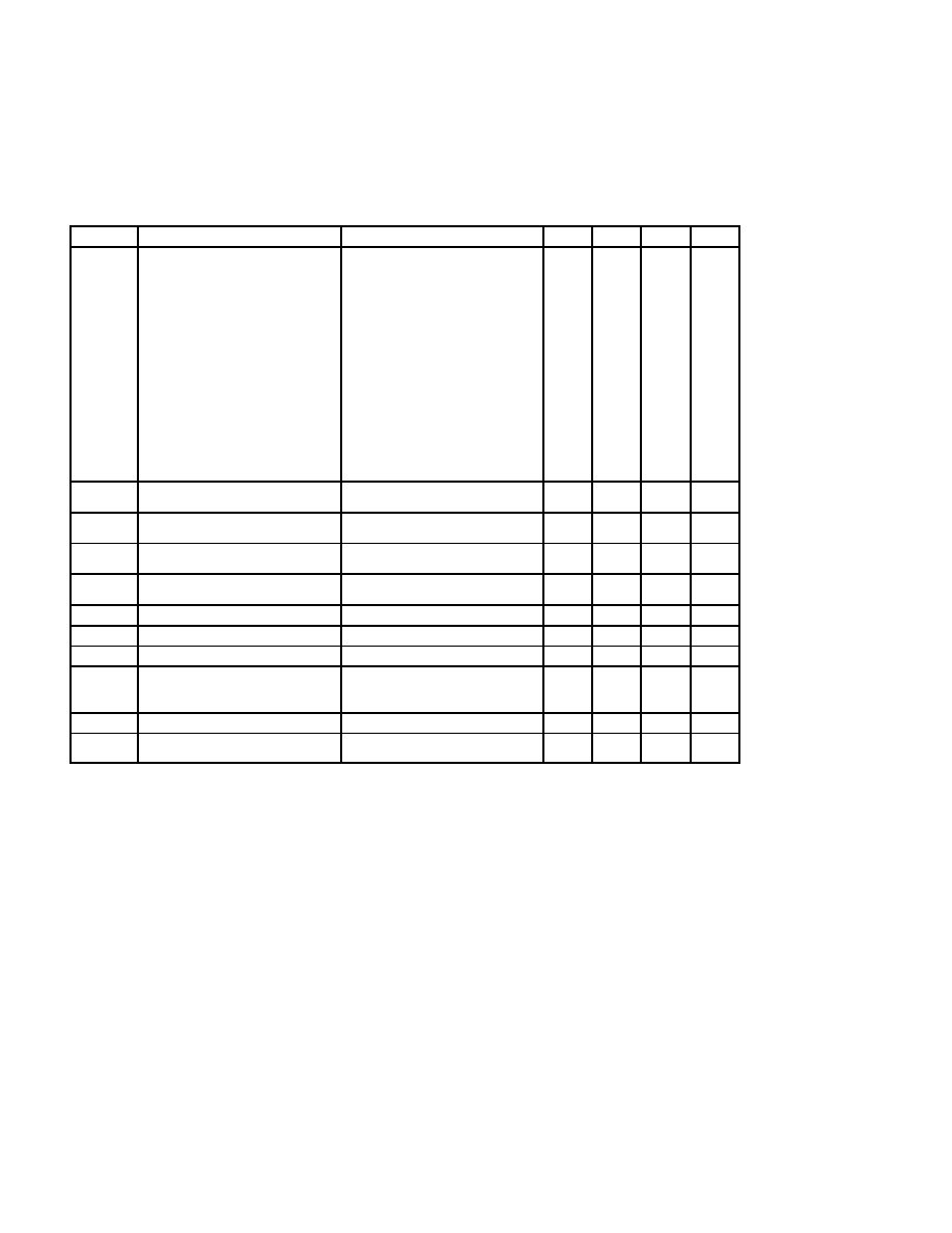
Absolute Maximum Ratings
(Note 1)
SYMBOL PARAMETER
Value
UNITS
VPP, VNN
Supply Voltage (Note 2)
+/-200
V
V5
Positive 5V Controller Voltage
Voltage at Input Pins (pins 4-8, 10-11)
6
-0.3 to (V5+0.3)
V
V
VN12
Voltage for FET drive
VNN+18
V
T
A
Operating Free-air Temperature Range
0∫ to 70∫
C
T
J
Junction Temperature
150∫
C
T
STORE
Storage Temperature Range
-40∫ to 150∫
C
ESD
HB
ESD Susceptibility ≠ Human Body Model (Note 3)
All Pins
2000
V
ESD
MM
ESD Susceptibility ≠ Machine Model (Note 4)
All Pins
200
V
Note 1: Absolute Maximum Ratings indicate limits beyond which damage to the device may occur.
See the table below for Operating Conditions.
Note 2: Limits based on components used inside the hybrid module. The internal over current circuit is not capable of
working above +/-130V due to bias level. An external over current circuit must be implemented for operation above
+/-130V. In most cases, the TA0105A is the best choice for operation above +/130V. A data sheet for the
TA0105A can be found on the Tripath website at www.tripath.com.
Note 3: Human body model, 100pF discharged through a 1.5K
resistor.
Note 4: Machine model, 220pF ≠ 240pF discharged through all pins.
Operating Conditions
(Note 5)
SYMBOL PARAMETER MIN.
TYP.
MAX.
UNITS
VPP, VNN
Supply Voltage (Note 5)
+/-125 +/-148 +/-185 V
V5
Positive 5V Controller Voltage
4.5
5
5.5
V
VN12
Voltage for FET drive (Volts about VNN)
10.8
12
13.2
V
Note 5: The VPP and VNN supply limits are based on the internal OV/UV sensing resistor values. The supply voltage
range can be lowered via external resistors. In the typical application of the TDA2500, the external resistors R
VPP1
,
R
VPP2
, R
VNN1
and R
VNN2
will be implemented, allowing operation down to +/-20V, if needed, to emulate previous
Tripath hybrid drivers. Please refer to the Application information section for a detailed discussion of changing the
operating supply voltage range and emulating such devices as TA0104A, TA0103A and TA0102A.

T r i p a t h T e c h n o l o g y, I n c . - T e c h n i c a l I n f o r m a t i o n
3
TDA2500 ≠ KL/ Rev. 0.9/05.05
Electrical Characteristics
(Note 6)
T
A
= 25
∞C. See Application/Test Circuit on page 7. Unless otherwise noted, the supply voltage is
VPP=|VNN|=90V. See Note 9.
SYMBOL PARAMETER
CONDITIONS MIN.
TYP.
MAX.
UNITS
I
q
Quiescent Current
(No load, BBM0=0,BBM1=1,
Mute = 0V)
VPP = +90V
VNN = -90V
V5 = 5V
VN12 = 12V
45
45
45
190
mA
mA
mA
mA
I
MUTE
Mute Supply Current
(No load, Mute = 5V)
VPP = +90V
VNN = -90V
V5 = 5V
VN12 = 12V
1
1
20
1
30
mA
mA
mA
mA
I
Po
Power Supply Current
(Po = 500W, R
L
= 4
)
VPP = +90V (Both Channels On)
VNN = -90V (Both Channels On)
7.05
7.05
A
A
V
IH
High-level input voltage (MUTE)
3.5
V
V
IL
Low-level input voltage (MUTE)
1.0
V
V
OH
High-level output voltage (HMUTE) RL = 10kohm
3.5
V
V
OL
Low-level output voltage (HMUTE) RL = 10kohm
0.5
V
V
OFFSET
Output Offset Voltage
No Load, MUTE = Logic low,
Measured without external trim
circuit connected, 1% R
FB
matching
-1.25 1.25 V
I
OC
Over Current Sense Voltage
Threshold
Exceeding this threshold causes a
latched mute condition
0.85 0.97 1.09 V
V
VPPSENSE
VPP Threshold Voltages
(Internal setting)
Over-voltage turn on (muted)
Over-voltage restart (mute off)
Under-voltage restart (mute off)
Under-voltage turn on (muted)
193
185
80
227
216
111
101
250
125
118
V
V
V
V
V
VNNSENSE
VNN Threshold Voltages
(Internal setting)
Over-voltage turn on (muted)
Over-voltage restart (mute off)
Under-voltage restart (mute off)
Under-voltage turn on (muted)
-193
-185
-80
-221
-215
-110
-98
-250
-125
-118
V
V
V
V
V
VPPSENSE
VPP Threshold Voltages
(Externally shifted)
(Note 7)
Over-voltage turn on (muted)
Over-voltage restart (mute off)
Under-voltage restart (mute off)
Under-voltage turn on (muted)
98
93
42
111
106
54
49
123
60
55
V
V
V
V
V
VNNSENSE
VNN Threshold Voltages
(Externally shifted)
(Note 7)
Over-voltage turn on (muted)
Over-voltage restart (mute off)
Under-voltage restart (mute off)
Under-voltage turn on (muted)
-96
-93
-40
-108
-105
-53
-48
-120
-60
-55
V
V
V
V
Note 6: Minimum and maximum limits are guaranteed but may not be 100% tested.
Note 7: These voltage values are calculated and not 100% tested. The voltages are based on 100% tested
sense currents, the internal over-voltage and under-voltage resistors, and external "shift" resistors as
follows: RVPP1 = RVPP2 = 1.33M
, RVNN1 = 1.21M and RVNN2 = 3.57 M. In addition, worse
case resistor tolerances (+/-1%) were used to calculate the minimum and maximum values. Please
refer to the Over-voltage and Under-voltage Protection section of the Applications Information on how
to set the operating voltage supply range.
T r i p a t h T e c h n o l o g y, I n c . - T e c h n i c a l I n f o r m a t i o n
4
TDA2500 ≠ KL/ Rev. 0.9/05.05
Electrical Characteristics
(Notes 8 and 9)
T
A
= 25
∞C. Unless otherwise noted, the supply voltage is VPP=|VNN|=90V, the input frequency is
1kHz and the measurement bandwidth is 20kHz. See Application/Test Circuit.
Note 8: Minimum and maximum limits are guaranteed but may not be 100% tested.
Note 9: Specific Components used:
Output MOSFETs (Q
O
): ST Microelectronics STW34NB20
Feedback Resistors (R
FB
): 18.7K
, 1%, 1W
Output Diodes (D
O
): International Rectifier MUR420
SYMBOL PARAMETER
CONDITIONS MIN.
TYP.
MAX.
UNITS
P
OUT
Output
Power
(Continuous Output/Channel)
VPP=|VNN|=90V, R
L
= 4
THD+N=10%
THD+N=1%
THD+N=0.1%
VPP=|VNN|=90V, R
L
= 8
THD+N=10%
THD+N=1%
THD+N=0.1%
VPP=|VNN|=75V, R
L
= 4
THD+N=10%
THD+N=1%
THD+N=0.1%
VPP=|VNN|=75V, R
L
= 8
THD+N=10%
THD+N=1%
THD+N=0.1%
1100
800
650
550
425
350
800
600
500
425
325
275
W
W
W
W
W
W
W
W
W
W
W
W
THD + N
Total Harmonic Distortion Plus
Noise
f = 1kHz, R
L
= 8
,
P
OUT
= 50W/Channel
0.015 %
THD + N
Total Harmonic Distortion Plus
Noise
f = 1kHz, R
L
= 4
,
P
OUT
= 50W/Channel
0.02 %
IMD Intermodulation
Distortion
19kHz, 20kHz, 1:1, R
L
= 8
P
OUT
= TBDW/Channel
0.02 %
SNR Signal-to-Noise
Ratio
A-Weighted, R
L
= 4
,
P
OUT
= 500W/Channel
103 dB
CS Channel
Separation
0dBr = 10W, R
L
= 4
, f = 1kHz
87 dB
Power Efficiency
P
OUT
= 300W/Channel, R
L
= 8
88 %
Power Efficiency
P
OUT
= 500W/Channel, R
L
= 4
79 %
A
V
Amplifier
Gain
P
OUT
= 10W/Channel, R
L
= 8
, Rin
= 49.9k
, See Application / Test
Circuit
14.6 V/V
A
VERROR
Channel to Channel Gain Error
P
OUT
= 10W/Channel, R
L
= 8
-1 1 dB
e
NOUT
Output Noise Voltage
A-Weighted, input shorted, DC
offset nulled to zero
325
µV

T r i p a t h T e c h n o l o g y, I n c . - T e c h n i c a l I n f o r m a t i o n
5
TDA2500 ≠ KL/ Rev. 0.9/05.05
TDA2500 Pinout
9
10
11
12
13
14
15
16
17
18
19
1
2
3
4
5
6
7
8
AGND
OVERLOADB
V5
IN2
IN1
BBM0
BBM1
MUTE
38
37
36
35
34
33
32
31
30
29
28
27
26
25
24
23
22
21
20
LO2
HO2COM
HO2
VNN
VPP
HO1
H01COM
LO1
G
ND K
E
L
V
I
N1
O
CR2
O
CR1
G
ND K
E
L
V
I
N2
OCS
1LP
OCS
1LN
OC
S
1
H
N
OC
S
1
H
P
LO1COM
F
D
BKN
1
VN
1
2
VL
O
W
VH
I
G
H
NC
HM
UTE
OC
S
2
H
P
OC
S
2
H
N
OC
S
2
L
P
OC
S
2LN
LO2C
O
M
F
D
BKN
2
PG
N
D