
C482, C484, and C486 (C48-Type)
2.5 Gb/s Cooled Laser Transmitters
Data Sheet, Rev. 3.0
November 2003
Offering multiple output power options and SONET/SDH com-
patibility, the C48-Type 2.5 Gb/s Cooled Laser Transmitters are
manufactured in a 24-pin plastic DIP with a single-mode fiber
pigtail.
Features
Data rates to 2.5 Gb/s
Two-channel selectable at 100 GHz spacing
SONET and ITU-T compliant at OC-48 and
STM-16
Cooled, InGaAsP MQW-DFB laser
Wavelength range, 1528.77 nm--1563.86 nm
User-selectable wavelengths
Clocked or nonclocked operation with single-ended
inputs; clocked operation with differential input
50
ac-coupled PECL compatible data and clock
inputs
Operation from 3.3 V and 5 V power supplies
Low-profile, 24-pin package
Automatic optical power control
Wide operating case temperature range,
�15 �C to +70 �C
Laser bias monitor alarm/laser degrade alarm
Laser back-facet monitor output
Transmitter-enable input
FC/PC, SC/PC, LU or MU connectors
Applications
Telecommunications:
-- SONET/SDH SR/IR/LR
-- Subscriber loop
-- Metropolitan area networks
High-speed data communications
Description
The C48-type 2.5 Gb/s cooled laser transmitters are
designed for use in transmission systems and high-
speed data communication applications. The transmit-
ter operates at the SONET OC-48 rate, as well as the
ITU-T SDH rate of STM-16. The device supports two
wavelengths. The second wavelength is selectable via
pin 10.
The transmitters meet all present Telcordia Technolo-
gies
TM
GR-253-CORE requirements and the ITU-T
G.957 and G.958 recommendations. They are also ide-
ally suited for extended-distance data and networking
applications.
Manufactured in a 24-pin DIP, the transmitter incorpo-
rates a hermetic multiquantum well (MQW) isolated
1550 nm digital distributed feedback (DFB) laser
(D2526 versions), an InGaAs PIN photodiode back-
facet monitor, and a GaAs laser driver IC. The unit
uses two power supplies. The laser transmitter
requires 5 V, and the thermoelectric cooler (TEC)
requires 3.3 V. The clock may be enabled for those
applications where jitter is critical.
Pin information is listed in Table 1.
�
riQ
T
uint
OPT
OEL
ECT
RON
ICS
Tran
smi
tter
C48
Ser
ies

2
2
For additional information and latest specifications, see our website: www.triquint.com
C482, C484, and C486 (C48-Type)
Data Sheet, Rev. 3.0
2.5 Gb/s Cooled Laser Transmitters
November 2003
Transmitter Processing
The transmitter can withstand normal wave soldering
processes. The complete transmitter module is not her-
metically sealed; therefore, it should not be immersed
in, or sprayed with, any cleaning solution or solvents.
The process cap and fiber pigtail jacket can deform at
temperatures greater than 85 �C. The transmitter pins
can be wave-soldered at a maximum temperature of
250 �C for 10 seconds.
Installation Considerations
Although the transmitter has been designed with rug-
gedness in mind, care should be used during handling.
The optical connector should be kept free from dust,
and the process cap should be kept in place as a dust
cover when the device is not connected to a cable. If
contamination is present on the optical connector, the
use of canned air with an extension tube should
remove any debris. Other cleaning procedures are
identified in the Cleaning Fiber-Optic Assemblies Tech-
nical Note (TN95-010LWP).
Connector Options
The standard fiber-optic pigtail is an 8
�m core single-
mode fiber in a 0.036 in. (914
�m) diameter, tight-buff-
ered outer jacket. The standard length is 39 in. � 4 in.
(1 m � 10 cm) and is terminated with an FC/PC,
SC/PC, LC, or MU optical connector. Other connector
options may be available on special order. Please con-
tact your Account Manager at TriQuint for ordering
information.
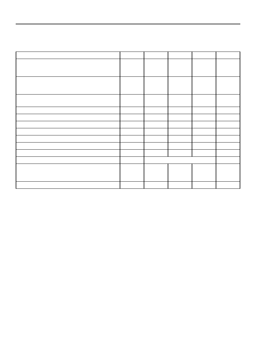
Table 1. Pin Descriptions
1. Laser back-facet (pin 2) and bias alarm functions (pin 3) are cus-
tomer-use options that are not required for normal operations of
the transmitter and are normally used during manufacture and for
diagnostics. Pin 3 output will optionally be either an analog bias
monitor (default) or a digital logic signal (LDA). (See Table 2.)
2. Pins designated no user connection (NUC) must not be tied to
ground or any other circuit potential.
3. When logic 0, the nominal channel wavelength (n) is selected;
when logic 1, the n � 1 channel wavelength is selected.
4. V
EE
is not used. This pin is NUC. The V
EE
labeling is maintained
for MSA purposes.
Pin Number
Name
1
Ground (TEC)
2
Back-facet Monitor
1
3
Bias Monitor/Laser Degrade Alarm
1
4
Tx Enable
5
Clock Select
6
Ground
7
Wavelength-Deviation Error Alarm
8
NUC
2
9
NUC
2
10
Wavelength Selection Command
3
11
Ground
12
V
EE4
13
V
CC
14
VTEC
(TEC supply voltage)
15
Ground
16
DATA
17
Ground
18
DATA
19
Ground
20
CLOCK
21
Ground
22
CLOCK
23
Ground
24
V
CC
Absolute Maximum Ratings
Stresses in excess of the absolute maximum ratings can cause permanent damage to the device. These are abso-
lute stress ratings only. Functional operation of the device is not implied at these or any other conditions in excess
of those given in the operations sections of the data sheet. Exposure to absolute maximum ratings for extended
periods can adversely affect device reliability.
Parameter
Symbol
Min
Max
Unit
Supply Voltage
--
--
5.25
V
Operating Case Temperature Range
T
C
�15
70
�C
Storage Case Temperature Range
T
stg
�40
85
�C
Lead Soldering Temperature/Time
--
--
250/10
�C/s
Relative Humidity (noncondensing)
RH
--
85
%
Minimum Fiber-bend Radius
--
1.00 (25.4)
--
in. (mm)
TEC Voltage
V
TEC
--
3.5
V

For additional information and latest specifications, see our website: www.triquint.com
3
Data Sheet, Rev. 3.0
C482, C484, and C486 (C48-Type)
November 2003
2.5 Gb/s Cooled Laser Transmitters
Characteristics
Minimum and maximum values specified over operating case temperature range at 50% duty cycle data signal.
Typical values are measured at room temperature unless otherwise noted.
1. Inputs are ac-coupled into an equivalent input impedance of 50
.
2. Single-ended or differential operation may used. If the inputs are driven single-ended, the unused inputs must be terminated in 50
.
3. Clocked operation is optional. For clocked operation, pin 5 must be a logic 0. With clocked operation, the optical output changes state with
the rising edge of the input clock signal.
4. If left unselected, clocked operation will be selected.
5.
N
is the ITU center wavelength, where N is the ITU frequency product designator ranging from 17 to 61. For example, if N = 23, then
N
= 1558.98 nm (f
N
= 192.3 THz) and
N � 1
= 1559.79 nm (f
N � 1
= 192.2 THz).
6. Deviation due to temperature variation detected by the thermistor.
7. This voltage is measured from pin 2 to GND.
8. Frequency range: 100 kHz--2 GHz.
9. At frequency of 2.5 GHz.
Table 2. Electrical Characteristics
Parameter
Symbol
Min
Typ
Max
Unit
dc Power Supply Voltage
V
CC
4.75
5.0
5.25
V
dc Power Supply Current:
C482, C484
C486
I
CC
I
CC
--
--
350
--
400
500
mA
mA
Power Dissipation
P
DIS
--
4.5
5.2
W
Input Data/Clock Voltage:
1, 2
Single-ended Input
Differential Input
V
IN
V
IN
250
125
900
450
1300
650
mVp-p
mVp-p
Nonclocked/Clocked Select Voltage:
3, 4
Clocked Operation
Nonclocked Operation
V
SEL_CLK
V
DIS_CLK
0.0
2.0
--
--
0.8
V
CC
V
V
Input Impedance
R
IN
--
50
--
Transmitter Enable Voltage (TTL) V
IL
V
EN
0.0
--
0.8
V
Transmitter Disable Voltage (TTL) V
IH
V
DIS
2.0
--
V
CC
V
Wavelength Selection Voltage (TTL) V
IL
5
V
N
0.0
--
0.8
V
Wavelength Selection Voltage (TTL) V
IH
5
V
N � 1
2.0
--
V
CC
V
Deviation Alarm:
Levels (CMOS) V
OL
Levels (CMOS) V
OH
Setting (active-high)
6
V
NO-
ALARM
V
ALARM
ALARM
0
4.5
�100
--
--
--
0.3
V
CC
100
V
V
pm
Laser Bias Monitor Voltage (default)
V
LBM
--
20
--
mV/mA
Laser Degrade Alarm (option):
Levels (CMOS) V
OH
Levels (CMOS) V
OL
Setting (active-low)
V
NO-ALARM
V
ALARM
LD
ALARM
4.5
0
--
--
--
--
V
CC
0.3
55
V
V
mA
Laser Back-facet Monitor Voltage (50% duty
cycle)
7
V
BF
--
500
--
mV/mW
Clock Duty Cycle
C
DC
40
50
60
%
TEC Current
I
TEC
--
0.6
1.2
A
TEC Voltage
V
TEC
3.0
3.3
3.5
V
Return Loss:
8,9
Input Data
Input Clock
RL
DATA
RL
CLK
�10
�12
--
--
--
--
dB
dB
4
For additional information and latest specifications, see our website: www.triquint.com
C482, C484, and C486 (C48-Type)
Data Sheet, Rev. 3.0
2.5 Gb/s Cooled Laser Transmitters
November 2003
Characteristics
(continued)
1. Output power definitions and measurement per ITU-T Recommendation G.957.
2. At room temperature; takes into account the initial variation in temperature as well as long-term aging. Please refer to the applica-
tion note, Wavelength Tolerance in DWDM for more information on this value.
3. Measured using time resolved spectroscopy (TRS). This corresponds to approximately 0.3 nm maximum at full width 20 dB down
using a spectrometer with resolution of 0.05 nm.
4.
Ratio of the average output power in the dominant longitudinal mode to the power in the most significant side mode under fully
modulated conditions.
5. Filter bandwidth from 12 kHz--20 MHz, according to ITU-T G813.
6. Ratio of logic 1 output power to logic 0 output under fully modulated conditions; with fourth-order Bessel-Thomson filter on.
7. GR-253-CORE, Synchronous Optical Network (SONET) Transport Systems: Common Generic Criteria.
8. ITU-T Recommendation G.957, Optical Interfaces for Equipment and Systems Relating to the Synchronous Digital Hierarchy.
Table 3. Optical Characteristics
Parameter
Symbol
Min
Typ
Max
Unit
Average Optical Power Output:
1
C482, C484
P
AVG BOL
P
AVG EOL
0
�0.5
1.0
--
2.0
2.0
dBm
dBm
Average Optical Power Output:
1
C486 P
AVG BOL
P
AVG EOL
6.0
5.5
6.7
--
8.0
8.5
dBm
dBm
Output Power Variation (over temperature and
wavelength)
P
�0.5
--
0.5
dBm
Center Wavelength Range (See Tables 6--21.)
C
1528.77
--
1563.86
nm
Wavelength Accuracy
2
C
�15
--
15
pm
Wavelength Variation and Aging
2
C
�100
--
100
pm
Wavelength Chirp (on-state/off-state
)
3
--
--
200
pm
Side-mode Suppression Ratio
4
SMSR
30
--
--
dB
Jitter, Intrinsic
5
--
--
--
0.05
UIp-p
Extinction Ratio
6
r
e
8.2
--
--
dB
Eye Mask of Optical Output
7, 8
--
Meets SONET and ITU-T
--
Optical Rise/Fall Time (20%--80%):
C482, C484
C486
t
R,
t
F
t
R,
t
F
--
--
--
--
130
150
ps
ps
Maximum Return Loss (optical)
O
RL
--
--
24
dB

For additional information and latest specifications, see our website: www.triquint.com
5
Data Sheet, Rev. 3.0
C482, C484, and C486 (C48-Type)
November 2003
2.5 Gb/s Cooled Laser Transmitters
Characteristics
(continued)
Figure 1. Data Timing Diagram
Table 4. Dispersion Performance
Parameter
Symbol
Test Conditions
Min
Typ
Max
Unit
Dispersion Penalty for Extended Reach:
C482, C486
C484
DP
DP
1800 ps/nm
3000 ps/nm
--
--
--
--
2.0
2.0
dB
dB
Table 5. Data Timing
Symbol
Setup (Min)
Hold (Min)
Unit
t1
35
--
ps
t2
--
60
ps
t1
t2
1/Bit Rate
DATA
DATA
CLOCK
t
t1
t2
1/Bit Rate
DATA
DATA
CLOCK
t