TriQuint Semiconductor Texas: Phone (972)994-8465 Fax (972)994 8504 Web: www.triquint.com
Product Data Sheet
November 19, 2003
TGA4501-SCC
1
Not Recommended for New Designs
TriQuint Recommends the TGA4505-EPU be used for New Designs
24-31 GHz Ka Band HPA
Primary Applications
∑
Satellite Ground Terminal
∑
Point-to-Point Radio
Key Features
∑
0.25 um pHEMT Technology
∑
23 dB Nominal Gain
∑
34.5 dBm Nominal P1dB
∑
40 dBm IMD3 Typical
∑
Bias 6 V @ 2.1 A
Chip Dimensions 4.3 mm x 3.0 mm x 0.05 mm
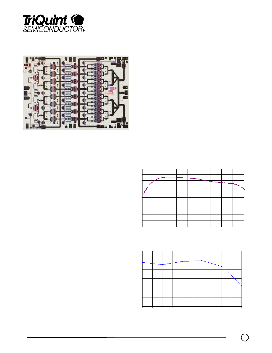
Fixtured Data
Bias Conditions: Vd = 6V, Id = 2.1A
±
5%
7
9
11
13
15
17
19
21
23
25
27
23
24
25
26
27
28
29
30
31
32
Frequency (GHz)
Gain (dB)
Product Description
The TriQuint TGA4501-SCC is a compact
3 Watt High Power Amplifier MMIC for
Ka-band applications. The part is
designed using TriQuint's proven
standard 0.25 um gate Power pHEMT
production process.
The TGA4501 provides a nominal 34.5
dBm of output power at 1 dB gain
compression from 24-31 GHz with a small
signal gain of 23 dB.
The part is ideally suited for low cost
emerging markets such as base station
transmitters for satellite ground terminals,
point to point radio and LMDS.
The TGA4501-SCC is 100% DC and RF
tested on-wafer to ensure performance
compliance.
25
27
29
31
33
35
37
27
27.5
28
28.5
29
29.5
30
30.5
31
31.5
32
Frequency (GHz)
P
out @
P
1
dB
(dB
m
)

TriQuint Semiconductor Texas: Phone (972)994-8465 Fax (972)994 8504 Web: www.triquint.com
Product Data Sheet
November 19, 2003
TGA4501-SCC
2
Not Recommended for New Designs
TriQuint Recommends the TGA4505-EPU be used for New Designs
TABLE I
MAXIMUM RATINGS
Symbol
Parameter 5/
Value
Notes
V
+
Positive Supply Voltage
8 V
4/
V
-
Negative Supply Voltage Range
-5V TO 0V
I
+
Positive Supply Current (Quiescent)
3.0 A
4/
| I
G
|
Gate Supply Current
62 mA
P
IN
Input Continuous Wave Power
24 dBm
P
D
Power Dissipation
18.4 W
3/ 4/
T
CH
Operating Channel Temperature
150
0
C
1/ 2/
T
M
Mounting Temperature
(30 Seconds)
320
0
C
T
STG
Storage Temperature
-65 to 150
0
C
1/
These ratings apply to each individual FET.
2/
Junction operating temperature will directly affect the device median time to failure (T
M
).
For maximum life, it is recommended that junction temperatures be maintained at the
lowest possible levels.
3/
When operated at this bias condition with a base plate temperature of 70
0
C, the median
life is reduced from 7.4 E+6 to 4.6 E+5 hours.
4/
Combinations of supply voltage, supply current, input power, and output power shall not
exceed P
D
.
5/
These ratings represent the maximum operable values for this device.
TriQuint Semiconductor Texas: Phone (972)994-8465 Fax (972)994 8504 Web: www.triquint.com
Product Data Sheet
November 19, 2003
TGA4501-SCC
3
Not Recommended for New Designs
TriQuint Recommends the TGA4505-EPU be used for New Designs
TABLE II
DC PROBE TEST
(TA = 25
∞
C, nominal)
LIMITS
NOTES
SYMBOL
MIN
MAX
UNITS
1/
I
DSS(Q35)
15
70.5
mA
1/
G
M (Q35)
33
79.5
mS
1/, 2/
|V
P(Q1, Q2, Q35)
|
0.5
1.5
V
1/, 2/
|V
BVGS(Q35)
|
8
30
V
1/, 2/
|V
BVGD(Q35)
|
11
30
V
1/ Q35 is a 150 um Test FET
2/ V
P
, V
BVGD
, and V
BVGS
are negative.
TriQuint Semiconductor Texas: Phone (972)994-8465 Fax (972)994 8504 Web: www.triquint.com
Product Data Sheet
November 19, 2003
TGA4501-SCC
4
Not Recommended for New Designs
TriQuint Recommends the TGA4505-EPU be used for New Designs
TABLE IV
THERMAL INFORMATION*
Parameter
Test Conditions
T
CH
(
o
C)
R
JC
(
∞
C/W)
T
M
(HRS)
R
JC
Thermal
Resistance
(channel to backside of
carrier)
Vd = 6V
I
D
= 2.048 A
Pdiss = 12.288 W
127.65
4.69
7.4E+6
Note: Assumes eutectic attach using 1.5 mil 80/20 AuSn mounted to a 20 mil
CuMo Carrier at 70
∞
C baseplate temperature. Worst case condition with no RF
applied, 100% of DC power is dissipated.
* This information is a result of a thermal model analysis.
TABLE III
RF CHARACTERIZATION TABLE
(T
A
= 25
∞
C, nominal)
(Vd = 6V, Id = 2.1A
±
5%)
LIMITS
SYMBOL
PARAMETER
TEST
CONDITION
MIN
TYP
MAX
UNITS
Gain
Small Signal
Gain
F = 24-31 GHz
18
23
dB
IRL
Input Return Loss
F = 24-31 GHz
---
-6
----
dB
ORL
Output Return
Loss
F = 24-31 GHz
---
-12
---
dB
PWR
Output Power @
P1dB
F = 27-31 GHz
34
35
---
dBm
IMR3
IMR3 @ SCL =
P1dB ≠ 10dB
F = 30 GHz
---
29
---
dBc
IMD3
Output IMD3
F = 30 GHz
Pin = 0 dBm
---
40
---
dBc
Note: Table III Lists the RF Characteristics of typical devices as determined by
fixtured measurements.
TriQuint Semiconductor Texas: Phone (972)994-8465 Fax (972)994 8504 Web: www.triquint.com
Product Data Sheet
November 19, 2003
TGA4501-SCC
5
Not Recommended for New Designs
TriQuint Recommends the TGA4505-EPU be used for New Designs
Fixtured Data
7
9
11
13
15
17
19
21
23
25
27
23
24
25
26
27
28
29
30
31
32
Frequency (GHz)
Ga
in
(d
B
)
Bias Conditions: Vd = 6 V, Id = 2.1 A
±
5%
25
27
29
31
33
35
37
27
27.5
28
28.5
29
29.5
30
30.5
31
31.5
32
Frequency (GHz)
Pout @ P1
dB (dBm)