8810
TGA8810-SCC
Gain Block Amplifier
q
2 to 10 -GHz Frequency Range
q
Operates from Single 5 -V Supply
q
Unconditionally Stable
q
17-dB Typical Gain
q
Typical ± 0.6-dB Gain Flatness
q
1,8796 x 1,6510 x 0,1524 mm (0.074 x 0.065 x 0.006 in.)
The TriQuint TGA8810 -SCC is a self-biased general purpose amplifier. Two gain stages
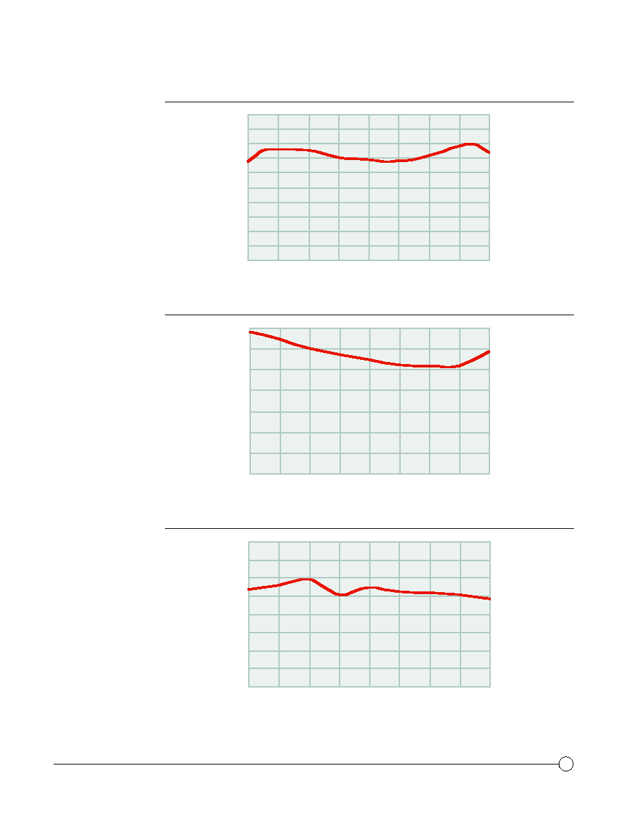
employ shunt feedback to pr oduce flat gain to 10 -GHz. Output power at 1- dB gain compression is
typically 17-dBm and noise figur e is 6 -dB. The TGA8810 -SCC uses on -chip DC blocks to allow dir ect
cascading. Three dif ferent on-chip self-bias resistors provide the flexibility of selecting bias cur rent
and RF per formance.
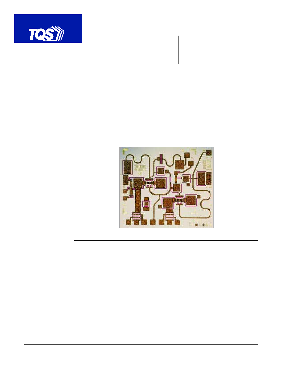
The TGA8810-SCC is available in chip for m and is r eadily assembled using automated equipment.
Bond pad and backside metallization is gold plated for compatibil ity with eutectic alloy attachment
methods as well as the ther mocompression and thermosonic wire-bonding processes.
DESCRIPTION
PHOTO ENLARGEMENT
O R , I N C .
T R I Q U I N T
S E M I C O N D U C T
TriQuint Semiconductor, Inc.
∑ Texas Facilities
∑ (972) 995-8465
∑ www.triquint.com
TGA8810-SCC
2
TYPICAL
SMALL SIGNAL
POWER GAIN
10
11
12
13
14
15
16
17
18
19
20
2
3
4
5
6
7
8
9
10
Frequency (GHz)
Gain (dB)
V
D1
= 5 V
V
D2
= 5 V
T
A
= 25∞
C
TYPICAL
NOISE FIGURE
0
1
2
3
4
5
6
7
2
3
4
5
6
7
8
9
10
Frequency (GHz)
Noise Figure (dB)
V
D1
= 5 V
V
D2
= 5 V
T
A
= 25∞
C
TYPICAL
OUTPUT POWER
P
1dB
12
13
14
15
16
17
18
19
20
2
3
4
5
6
7
8
9
10
Frequency (GHz)
Output Power (dBm)
V
D1
= 5 V
V
D2
= 5 V
T
A
= 25∞
C
TriQuint Semiconductor, Inc.
∑ Texas Facilities
∑ (972) 995-8465
∑ www.triquint.com
TGA8810-SCC
3
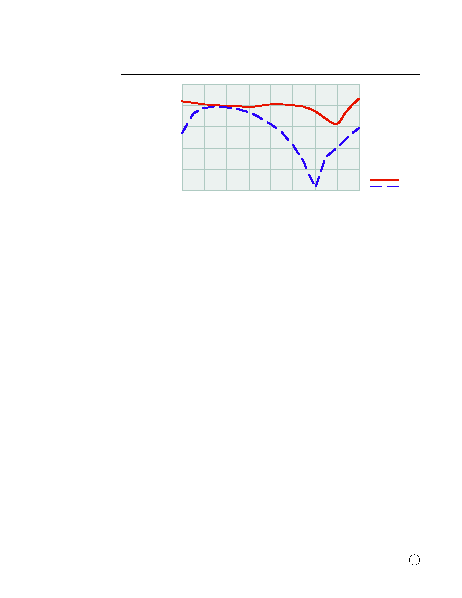
TYPICAL
RETURN LOSS
0
10
20
30
40
50
2
3
4
5
6
7
8
9
10
Frequency (GHz)
Return Loss (dB)
Input
Output
V
D1
= 5 V
V
D2
= 5 V
T
A
= 25∞
C
ABSOLUTE
MAXIMUM RATINGS
Positive supply voltage, V
D1
, V
D2
........................................................................................................
8.5 V
Power dissipation at (or below) 25∞C base -plate temperature, P
D
* ......................................................
2.4 W
Operating channel temperature, T
CH
** ......................................................... .....................................
150∞C
Mounting temperature (30 sec), T
M
..................................................................................................
320∞C
Storage temperature range, T
STG
............................................................................................
- 65 to 150∞C
Ratings over channel temperatur e range, T
CH
(unless otherwise noted)
Stresses beyond those listed under "Absolute Maximum Ratings" m ay cause per manent damage to the device.
These are stress ratings only, and functional operation of the device at these or any oth er conditions beyond
those indicated under "RF Characteristics" is not implied. E xposure to absolute maximum rated conditions for
extended periods may af fect device reliability.
* For operation above 25∞C base -plate temperature, derate linearly at the rate of 5 mW/∞C.
** Operating channel temperature, T
CH
, directly af fects the device MTTF. For maximum life, it is r ecommended
that channel temperature be maintained at the lowest possible level.
TriQuint Semiconductor, Inc.
∑ Texas Facilities
∑ (972) 995-8465
∑ www.triquint.com
TGA8810-SCC
4
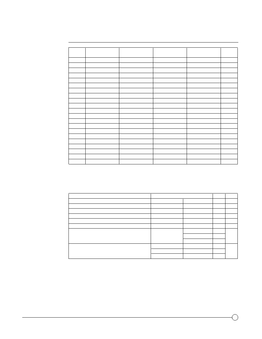
TYPICAL S-PARAMETERS
Frequency
S
11
S
21
S
12
S
22
GAIN
(GHz)
MAG
ANG(∞)
MAG
ANG(∞)
MAG
ANG(∞)
MAG
ANG(∞)
(dB)
0.5
0.38
-104
0.03
-148
0.001
-13
0.92
-130
-30.8
1.0
0.29
-125
0.99
-177
0.003
180
0.79
165
-0.1
1.5
0.36
-134
4.24
114
0.009
122
0.48
111
12.5
2.0
0.40
-156
6.88
42
0.011
72
0.07
125
16.8
2.5
0.36
-169
7.49
-8
0.009
43
0.21
180
17.5
3.0
0.33
-173
7.58
-45
0.007
27
0.27
164
17.6
3.5
0.31
-175
7.59
-77
0.006
10
0.29
150
17.6
4.0
0.30
-175
7.53
-106
0.004
9
0.28
137
17.5
4.5
0.30
-176
7.36
-133
0.002
5
0.26
126
17.3
5.0
0.29
179
7.10
-157
0.002
2
0.22
115
17.0
5.5
0.31
-178
7.02
179
0.001
-53
0.17
109
16.9
6.0
0.33
179
6.98
156
0.001
-152
0.12
110
16.9
6.5
0.33
173
6.86
134
0.002
-178
0.07
111
16.7
7.0
0.32
166
6.90
113
0.003
169
0.04
120
16.8
7.5
0.29
156
7.01
90
0.004
173
0.02
140
16.9
8.0
0.23
140
7.22
67
0.005
168
0.00
2
17.2
8.5
0.15
110
7.48
43
0.007
177
0.02
0
17.5
9.0
0.11
33
7.75
15
0.009
175
0.03
24
17.8
9.5
0.24
-37
7.87
-15
0.011
170
0.06
52
17.9
V
D1
= V
D2
= 5 V, T
A
= 25∞C
Reference planes for S -parameter data include bondwir es as specified in the "Recommended Assembly
Diagram".
RF CHARACTERISTICS
V
D1
= V
D2
= 5 V, T
A
= 25∞C (assembled per Equivalent Schematic unless other wise noted)
PARAMETER
TEST CONDITIONS
TYP
UNIT
G
P
Small≠signal power gain
f = 2 to 10 GHz
17
dB
SWR(in)
Input standing wave ratio
f = 2 to 10 GHz
1.9:1
-
SWR(out) Output standing wave ratio
f = 2 to 10 GHz
1.2:1
-
P
1dB
Output power at 1≠dB gain compression
f = 2 to 10 GHz
17
dBm
NF
Noise figure
f = 2 to 10 GHz
6
dB
G
p
Gain flatness
f = 2 to 10 GHz
±0.6
dB
f = 2 GHz
-0.01
Gain temperature coefficient
T
BP
= -40∞C to 90∞C f = 6 GHz
-0.02
dB/∞C
f = 10 GHz
-0.02
f = 2 GHz
24
IP
3
Output third≠order intercept point
f = 5 GHz
26
dBm
f = 8 GHz
25
10.0
10.5
0.44
0.64
-75
-106
7.39
6.34
-49
-83
0.013
0.016
162
153
0.09
0.11
58
51
17.4
16.0
TriQuint Semiconductor, Inc.
∑ Texas Facilities
∑ (972) 995-8465
∑ www.triquint.com
TGA8810-SCC
5
RF Input
0.1 pF
C
1
C
2
0.2 pF
Bond Pad #2
V
D1
Bond Pad #3
V
D2
RF Output
FET 2
500 m
FET 1
500 m
5
9
6
5
9
6
R
S21
R
S23
R
S22
R
S12
R
S13
R
S11
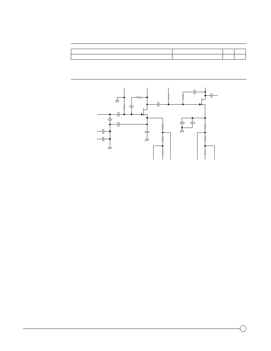
EQUIVALENT SCHEMATIC
DC CHARACTERISTICS
PARAMETER
TEST CONDITIONS
TYP
UNIT
I
D
= I
D1
+ I
D2
Total positive supply current
V
D1
= V
D2
= 5 V
90
mA
T
A
= 25∞C
R
S11
, R
S12
, R
S13
, R
S21
, R
S22
, and R
S23
provide the flexibility of selecting bias cur rent and RF per formance. C
1
and
C
2
can be used in tuning for impr oved input match. For best r esults, use the assembly configuration shown in
the "Recommended Assembly Diagram" on page 6.
TriQuint Semiconductor, Inc.
∑ Texas Facilities
∑ (972) 995-8465
∑ www.triquint.com
TGA8810-SCC
6
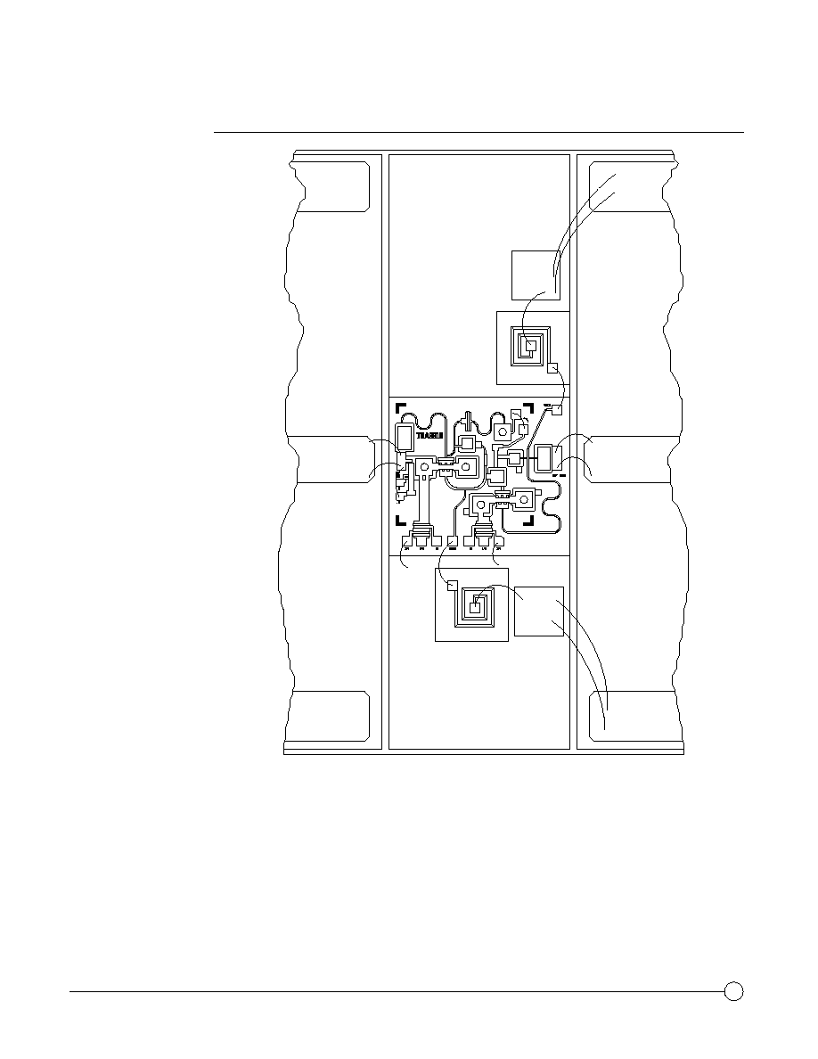
RECOMMENDED
ASSEMBLY DIAGRAM
V
D2
V
D1
RF Output
RF Input
T.I.P.N. 3022039-1
~2.3nH
68 pF
68 pF
T.I.P.N. 3022039-1
~2.3nH
RF connections: bond using two 1 -mil diameter, 20 to 25 -mil-length gold bond wir es at both RF Input and RF
Output for optimum RF per formance.
Close placement of exter nal components is essential to stability .
Bond using 0 .7 -mil diameter wires on bond pads 7, 11, 13, and 14 since they ar e less than the .004 x .004
needed for 1-mil diameter wire.
Two on-chip to on -chip wire bonds are needed for bond pads 1, 2, 3, and 13.
TriQuint Semiconductor, Inc.
∑ Texas Facilities
∑ (972) 995-8465
∑ www.triquint.com
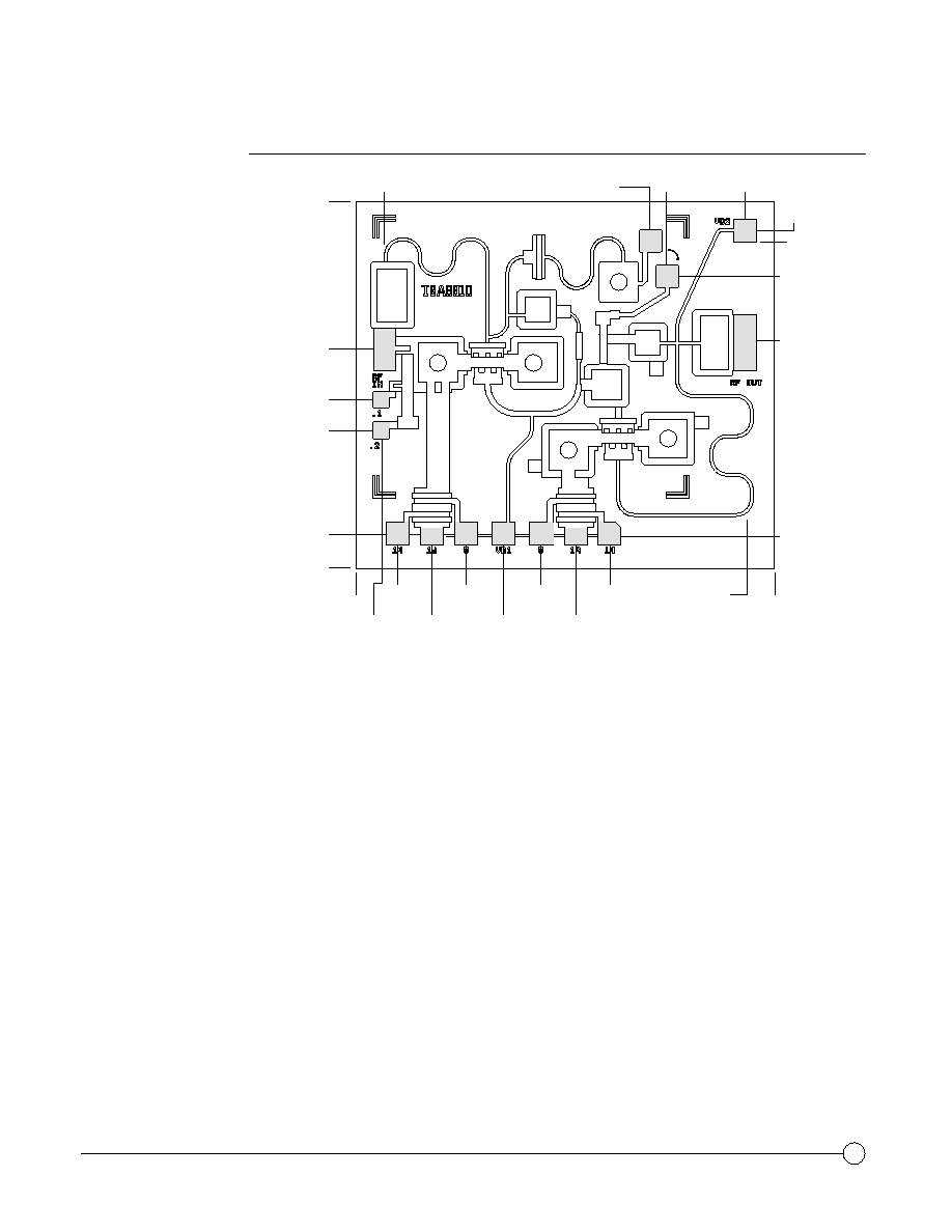
MECHANICAL DRAWING
7
TGA8810-SCC
0,1499
(0.0059)
1,5240
(0.0600)
1,4757
(0.0581)
1,3157
(0.0518)
1,0185
(0.0401)
1,6510
(0.0650)
0,9881
(0.0389)
0,7620
(0.0300)
0,6223
(0.0245)
0,1600
(0.0063)
0
1,7475
(0.0688)
1,3970
(0.0550)
1,3208
(0.0520)
0,1245
(0.0049)
(0.0740)
1,7501
(0.0689)
1,1379
(0.0448)
0,9855
(0.0388)
0,8306
(0.0327)
0,6604
(0.0260)
0,4953
(0.0195)
0,3378
(0.0133)
0,1854
(0.0073)
0,1118
(0.0044)
0
12
11
10
9
8
7
6
5
4
3
2
1
14
13
Units: millimeters (inches)
Thickness: 0,1524 (0.006) (r eference only)
Chip-edge-to-bond-pad dimensions are shown to center of bond pad.
Chip size tolerance: ± 0,0508 (0.002)
Bond pad #1 (RF Input):
0,1016 x 0,1778 (0.0040 x 0.0070)
Bond pad #2 :
0,1016 x 0,1016 (0.0040 x 0.0040)
Bond pad #3 :
0,1016 x 0,1016 (0.0040 x 0.0040)
Bond pad #4 (V
D2
):
0,1016 x 0,1016 (0.0040 x 0.0040)
Bond pad #5 (RF Output):
0,0940 x 0,2540 (0.0037 x 0.0100)
Bond pad #6 (R
S22
):
0,1016 x 0,1016 (0.0040 x 0.0040)
Bond pad #7 (R
S23
):
0,1016 x 0,0787 (0.0040 x 0.0031)
Bond pad #8 (R
S21
):
0,1067 x 0,1016 (0.0042 x 0.0040)
Bond pad #9 (V
D1
):
0,1016 x 0,1041 (0.0040 x 0.0041)
Bond pad #10 (R
S11
):
0,1067 x 0,1016 (0.0042 x 0.0040)
Bond pad #11 (R
S13
):
0,1016 x 0,0787 (0.0040 x 0.0031)
Bond pad #12 (R
S12
):
0,1016 x 0,1016 (0.0040 x 0.0040)
Bond pad #13 (C2):
0,0762 x 0,0762 (0.0030 x 0.0030)
Bond pad #14 (C1):
0,0762 x 0,0762 (0.0030 x 0.0030)
TriQuint Semiconductor, Inc.
∑ Texas Facilities
∑ (972) 995-8465
∑ www.triquint.com