TE100RS THRU TE108RS
GLASS PASSIVATED JUNCTION FAST SWITCHING RECTIFIER
VOLTAGE - 50 to 800 Volts CURRENT - 1.0 Ampere
FEATURES
l
Plastic package has Underwriters Laboratory
Flammability Classification 94V-O Utilizing
Flame Retardant Epoxy Molding Compound
l
Glass passivated junction
l
1 ampere operation at T
A
=55 with no thermal runaway
l
Exceeds environmental standards of MIL-S-19500/228
l
Fast switching for high efficiency
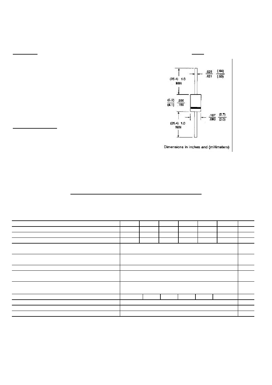
MECHANICAL DATA
Case: Molded plastic, A-405
Terminals: axial leads, solderable per MIL-STD-202,
Method 208
Polarity: Color band denotes cathode
Mounting Position: Any
Weight: 0.008 ounce, 0.22 gram
MAXIMUM RATINGS AND ELECTRICAL CHARACTERISTICS
Ratings at 25 ambient temperature unless otherwise specified.
Single phase, half wave, 60Hz, resistive or inductive load.
For capacitive load, derate current by 20%.
TE100RS TE101RS TE102RS TE104RS TE106RS TE108RS UNITS
Maximum Recurrent Peak Reverse Voltage
50
100
200
400
600
800
V
Maximum RMS Voltage
35
70
140
280
420
560
V
Maximum DC Blocking Voltage
50
100
200
400
600
800
V
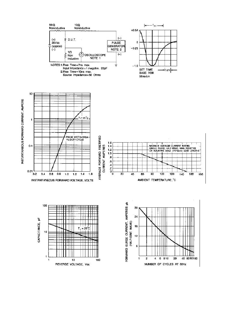
Maximum Average Forward Rectified Current
.375"(9.5mm) lead length at T
A
=55
1.0
A
Peak Forward Surge Current 8.3ms single half sine
wave superimposed on rated load(JECEC method)
30
A
Maximum Forward Voltage at 1.0A
1.3
V
Maximum Full Load Reverse Current Full Cycle
Average, .375",9.5mm Lead Length at T
A
=55
5.0
A
Maximum DC Reverse Current
at Rated DC Blocking Voltage T
A
=100
150
A
Maximum Reverse Recovery Time(Note 1)
150
150
150
150
250
500
ns
Typical Junction capacitance (Note 2)
15
P
F
Typical Thermal Resistance (Note 3) R JA
67
/W
Operating and Storage Temperature Range T
J
-55 to +150
NOTES:
1. Measured with I
F
=.5A, I
R
=1A, I
rr
=.25A
2. Measured at 1 MHz and applied reverse voltage of 4.0 VDC
3. Thermal resistance from junction to ambient at 0.375"(9.5mm) lead length P.C.B. mounted
A-405