- 406 -
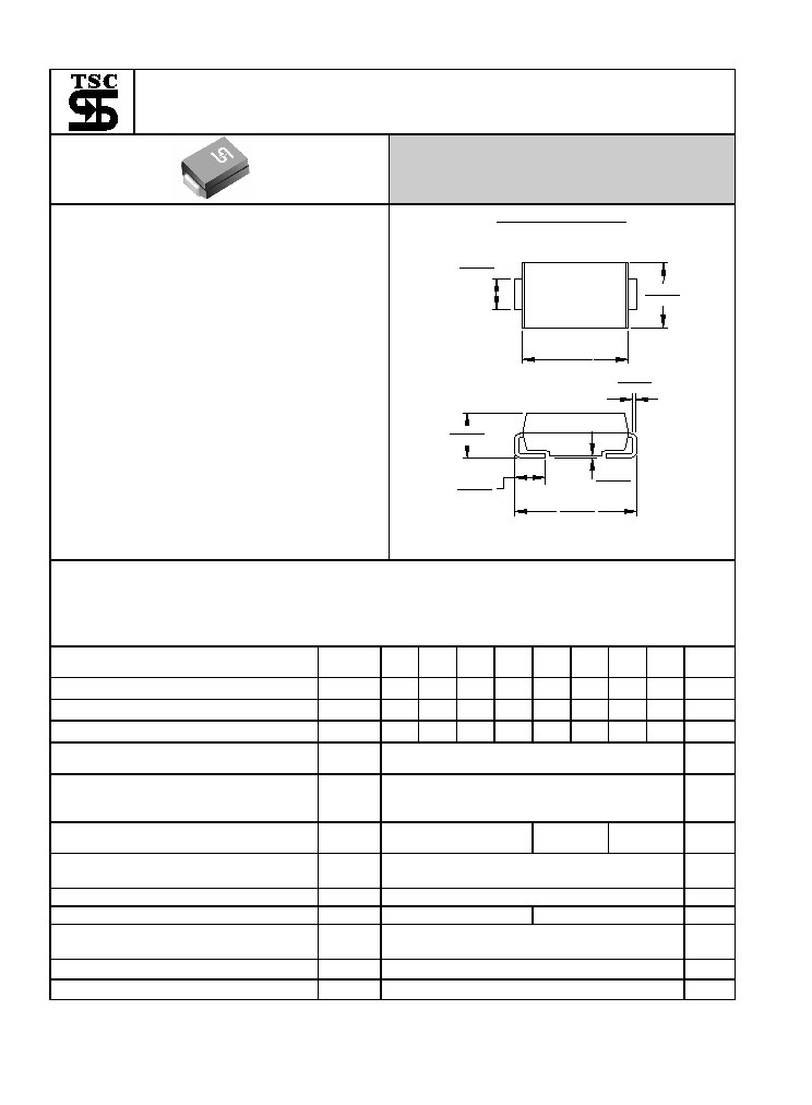
.129(3.27)
.118(3.0)
.012(.31)
.006(.15)
.008(.20)
.004(.10)
.060(1.52)
.030(0.76)
.245(6.22)
.220(5.59)
.280(7.11)
.260(6.60)
.103(2.62)
.079(2.00)
.320(8.13)
.305(7.75)
ES3A THRU ES3G
3.0 AMPS. Super Fast Surface Mount Rectifiers
Voltage Range
50 to 600 Volts
Current
3.0 Amperes
Features
a
Glass passivated junction chip
a
For surface mounted applications
a
Low profile package
a
Built-in strain relief
a
Ideal for automated placement
a
Easy pick and place
a
Superfast recovery time for high efficiency
a
Glass passivated chip junction
a
High temperature soldering:
260
O
C/10 seconds at terminals
a
Plastic material used carries Underwriters
Laboratory Classification 94V -O
Mechanical Data
a
Cases: Molded plastic
a
Terminals: Solder plated
a
Polarity: Indicated by cathode band
a
Packaging: 16mm tape per EIA STD RS-481
a
Weight: 0.21 gram
SMC/DO-214AB
Dimensions in inches and (millimeters)
Maximum Ratings and Electrical Characteristics
Rating at 25
+
ambient temperature unless otherwise specified.
Single phase, half wave, 60 Hz, resistive or inductive load.
For capacitive load, derate current by 20%
Type Number
Symbol
ES
3A
ES
3B
ES
3C
ES
3D
ES
3F
ES
3G
ES
3H
ES
3J
Units
Maximum Recurrent Peak Reverse Voltage
V
RRM
50 100 150 200 300 400 500 600
V
Maximum RMS Voltage
V
RMS
35
70 105 140 210 280 350 420
V
Maximum DC Blocking Voltage
V
DC
50 100 150 200 300 400 500 600
V
Maximum Average Forward Rectified Current
See Fig. 1
I
(AV)
3.0 A
Peak Forward Surge Current, 8.3 ms Single
Half Sine-wave Superimposed on Rated
Load (JEDEC method ) @T
L
= 100
+
I
FSM
100 A
Maximum Instantaneous Forward Voltage
@ 3.0A
V
F
0.95 1.3
1.7
V
Maximum DC Reverse Current @ T
A
=25
+
at Rated DC Blocking Voltage @ T
A
=100
+
I
R
10
500
uA
uA
Maximum Reverse Recovery Time ( Note 1 )
Trr 35 nS
Typical Junction Capacitance ( Note 2 )
Cj 45
30
pF
Typical Thermal Resistance (Note 3)
R
JA
R
JL
47
12
+
/W
Operating Temperature Range
T
J
-55 to +150
+
Storage Temperature Range
T
STG
-55 to + 150
+
Notes: 1. Reverse Recovery Test Conditions: I
F
=0.5A, I
R
=1.0A, I
RR
=0.25A
2. Measured at 1 MHz and Applied V
R
=4.0 Volts
3. Units Mounted on P.C.B. with 0.31 x 0.31"(8.0 x 8.0mm) Copper Pad Areas
REV.1 Oct.-2003
- 407 -
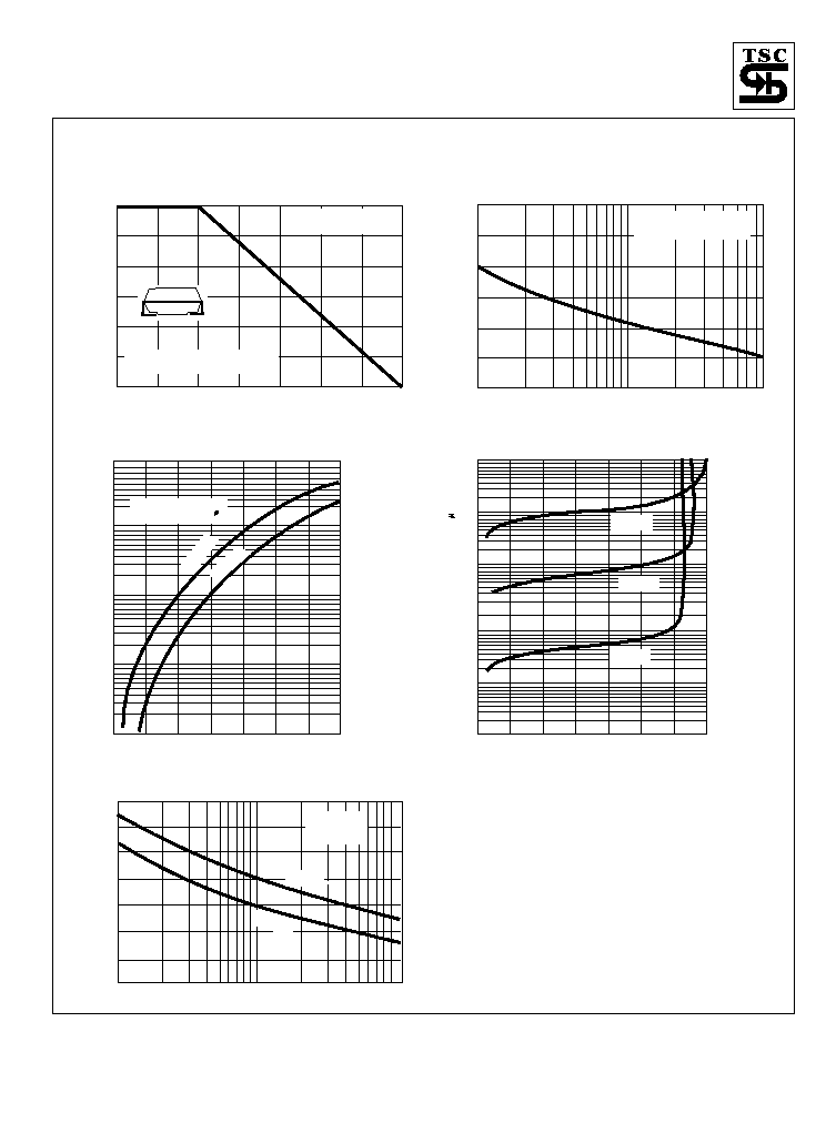
RATINGS AND CHARACTERISTIC CURVES (ES3A THRU ES3J)
FIG.2- MAXIMUM NON-REPETITIVE PEAK FORWARD
SURGE CURRENT
PEAK
FOR
W
ARD
SURGE
CURRENT
.
(A)
1
10
100
150
100
50
25
0
125
75
NUMBER OF CYCLES AT 60Hz
8.3ms Single Half Sine Wave
(JEDEC Method) at T =120 C
L
o
FIG.3- TYPICAL INSTANTANEOUS
FORWARD CHARACTERISTICS
INST
ANT
ANEOUS
FOR
W
ARD
CURRENT
.
(A)
0.4
0.6
0.8
1.0
1.2
1.4
1.6
1.8
0.01
1
10
100
0.1
FORWARD VOLTAGE. (V)
ES3A
- D
ES3F
- J
Tj=25 C
PULSE WIDTH-300 S
1% DUTY CYCLE
0
FIG.1- MAXIMUM FORWARD CURRENT DERATING
CURVE
A
VERAGE
FOR
W
ARD
CURRENT
.
(A)
80
90
100
120
140
150
130
110
0
2.0
3.0
1.0
LEAD TEMPERATURE. ( C)
o
RESISTIVE OR
INDUCTIVE LOAD
P.C.B. MOUNTED ON
0.31X0.31"(8.0X8.0mm) COPPER PADS
FIG.4- TYPICAL REVERSE CHARACTERISTICS
INST
ANT
ANEOUS
REVERSE
CURRENT
.(
A
)
0
20
40
60
80
100
120
140
10
100
1000
1
0.1
0.01
PERCENT OF RATED PEAK REVERSE VOLTAGE. (%)
Tj=100 C
0
Tj=75 C
0
Tj=25 C
0
10
1
0
100
105
75
45
30
15
90
60
FIG.5- TYPICAL JUNCTION CAPACITANCE
JUNCTION
CAP
ACIT
ANCE.(pF)
REVERSE VOLTAGE. (V)
ES3A
- D
ES3F
- J
Tj=25 C
f=1.0MHz
Vsig=50mVp-p
0