 | ÐлекÑÑоннÑй компоненÑ: TS258CS | СкаÑаÑÑ:  PDF PDF  ZIP ZIP |
Äîêóìåíòàöèÿ è îïèñàíèÿ www.docs.chipfind.ru
TS258
1-6
2005/02 rev. A
TS258
Dual Operating Amplifier
Supply Voltage Range 3 V to 32V
Dual Channel Amplifier
General Description
Utilizing the circuit designs perfected for recently introduced Quad Operational Amplifiers, these dual operational
amplifiers have several distinct advantages over standard operational amplifier types in single supply applications. They
can operate at supply voltages as low as 3.0 Volts or as high as 32 Volts with quiescent currents about one fifth of those
associated with the LM741 (on a pet amplifier basis). The common mode input range includes the negative supply,
thereby eliminating the necessity for external biasing components in many applications.
The TS258 is equivalent to one half of TS224, and output voltage range also includes the negative supply voltage.
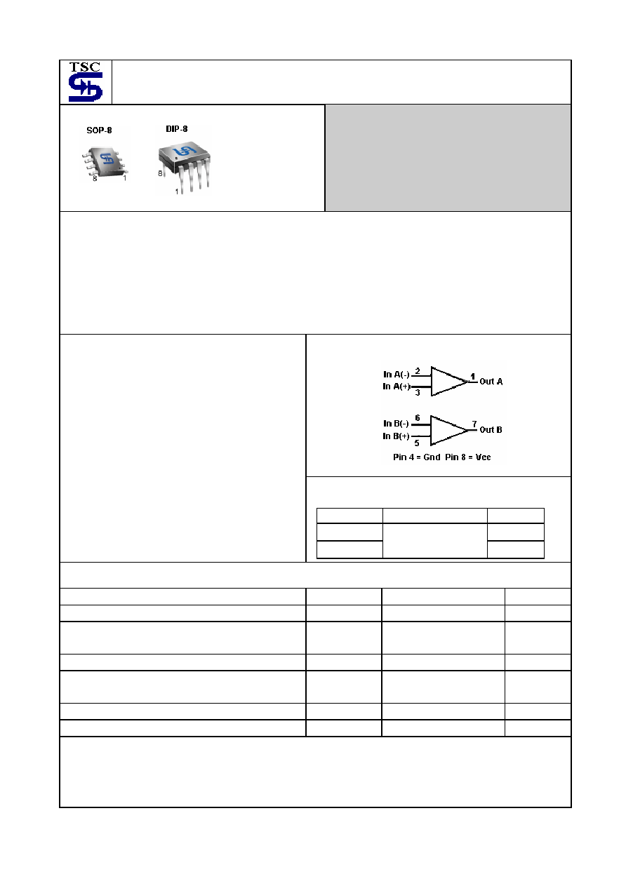
The TS258 is offered in 8 pin SOP-8 and DIP-8 package.
Block Diagram
Features
Short circuit protected outputs
True differential input stage
Single supply operation: 3V to 32V
Low input bias currents
Internally
compensated
Common mode range extends to negative supply
Single and split supply operation
Similar performance to the popular MC1558
Ordering Information
Part No.
Operating Temp. Package
TS258CD DIP-8
TS258CS
-40 ~ +85
o
C
SOP-8
Absolute Maximum Rating
Supply Voltage
Vcc, Vcc/Vee
+32 or ±16
Vdc
Differential Input Voltage (note 1)
V
IDR
32 Vdc
Input Common Mode Voltage Range (note 2)
Input Forward Current (note 3)
V
ICR
Iif
-0.3 to 32
50
Vdc
mA
Output Short Circuit Duration
Isc
Continuous
mA
Power Dissipation @ Ta=25
o
C
Derate above 25
o
C
1/Rja
570
5.7
mW
mW/
o
C
Operating Junction Temperature Range
T
J
0 ~ +125
o
C
Storage Temperature Range
T
STG
-65 ~ +150
o
C
NOTE :
1. Split Power Supplies.
2. For supply. Voltages less than 32V for the PJ358 the absolute maximum input voltage is equal to the supply voltage.
3. This input current will only exist when the voltage is negative at any of the input leads. Normal output states will
reestablish when the input voltage returns to a voltage greater than -0.3V.
Pin assignment:
1. Output
2. Input A (-)
3. Input A (+)
4. Gnd
5. Input B (+)
6. Input B (-)
7. Output B
8. Vcc
TS258
2-6
2005/02 rev. A
Electrical Characteristics
(V
CC
= 5V, Ta=25
o
C; unless otherwise specified.)
Characteristics Symbol
Min
Typ
Max
Unit
Input Offset Voltage
V
CC
= 5.0V to 30V, V
IC
= 0V to Vcc -1.7 V, Vo= 1.4V, R
S
= 0
T
LOW
Ta
T
HIGH
Vio
--
--
2.0
--
5.0
7.0
mV
Average Temperature Coefficient of Input Offset Voltage
Iio/ T
-- 7.0 --
uV/
o
C
Input Offset Current
T
LOW
Ta
T
HIGH
Iio --
--
5.0
--
50
150
nA
Average Temperature Coefficient of input Offset Current
Iio/ T
-- 10 --
pA/
o
C
Input Bias Current
T
LOW
Ta
T
HIGH
I
IB
--
45
50
-250
-500
uA
Input Common-Mode Voltage Range (Note1)
V
CC
= 30 V
V
CC
= 30 V, T
LOW
Ta
T
HIGH
V
ICR
0
0
--
--
28.3
28
V
Differential Input Voltage Range
V
IDR
-- -- V
CC
V
Large Signal Open-Loop Voltage Gain
R
L
= 2.0K, V
CC
=15V, For Large V
O
Swing,
T
LOW
Ta
T
HIGH
A
VOL
25
15
100
--
--
--
V/mV
Channel Separation
1.0 KHz to 20KHz
-- --
-120
--
dB
Common Mode Rejection Ratio
R
S
10 k
CMRR 65 70 --
dB
Power Supply Rejection Ratio
PSRR
65
100
--
dB
Output Voltage Range, RL = 2K
V
OR
0 -- 3.3 V
Output Voltage -- High Limit
V
CC
= 30 V, R
L
= 2 k
V
CC
= 30 V, R
L
= 10 k
V
OH
26
27
--
28
--
--
V
Output Voltage -- Low Limit
V
CC
= 5.0 V, R
L
= 10 k
V
OL
-- 5.0
20
mV
Output Source Current V
ID
=+1.0V,V
CC
=15V I
O+
20 40 -- mA
Output Sink Current
V
ID
= -1.0 V, V
CC
= 15 V
V
ID
= -1.0 V, V
O
= 200 mV
I
O-
10
12
20
50
--
--
mA
uA
Output Short Circuit to Ground (Note 2)
I
OS
-- 40
60
mA
Power Supply Current ,
V
CC
= 30 VV
O
= 0 V, R
L
=
V
CC
= 5.0 V, V
O
= 0 V, R
L
=
I
CC
--
--
1.5
0.7
3.0
1.2
mA
Notes :
1. The input common mode voltage or either input signal voltage should not be allowed to go negative by more than
0.3 V. The upper end of the common mode voltage range is Vcc 17V, but either or both inputs can go to +32V.
2. Short circuits from the output to Vcc can cause excessive heating and eventual destruction. Destructive dissipation
can recruit from simultaneous shorts on all amplifiers.
TS258
3-6
2005/02 rev. A
Circuit Description
The TS258 made using two internally compensated, two-stage operational amplifiers. The first stage performs not
only the first stage gain function but also performs the level shifting and transconductance reduction functions. By
reducing the transconductance, a smaller compensation capacitor (only 5.0pF) can be employed, thus saving chip
area. Another feature of this input stage is that the input common mode range can include the negative supply or
ground, in single supply operation, without saturating either the input devices or the differential to single-ended
converter. The second stage consists of a standard current source load amplifier stage.
Each amplifier is biased from an internal-voltage regulator, and which has a low temperature coefficient thus giving
each amplifier good temperature characteristics as well as excellent power supply rejection.
TS258
4-6
2005/02 rev. A
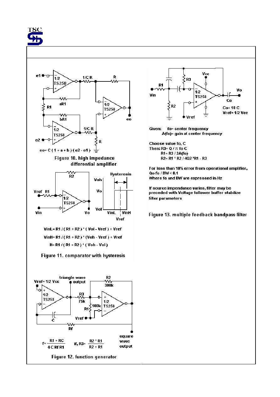
Circuit Description
TS258
5-6
2005/02 rev. A
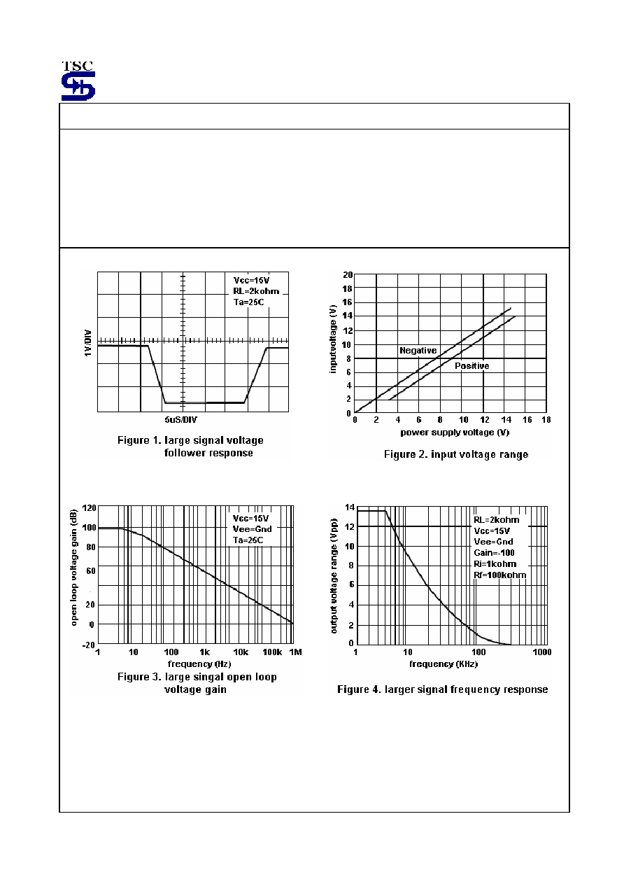
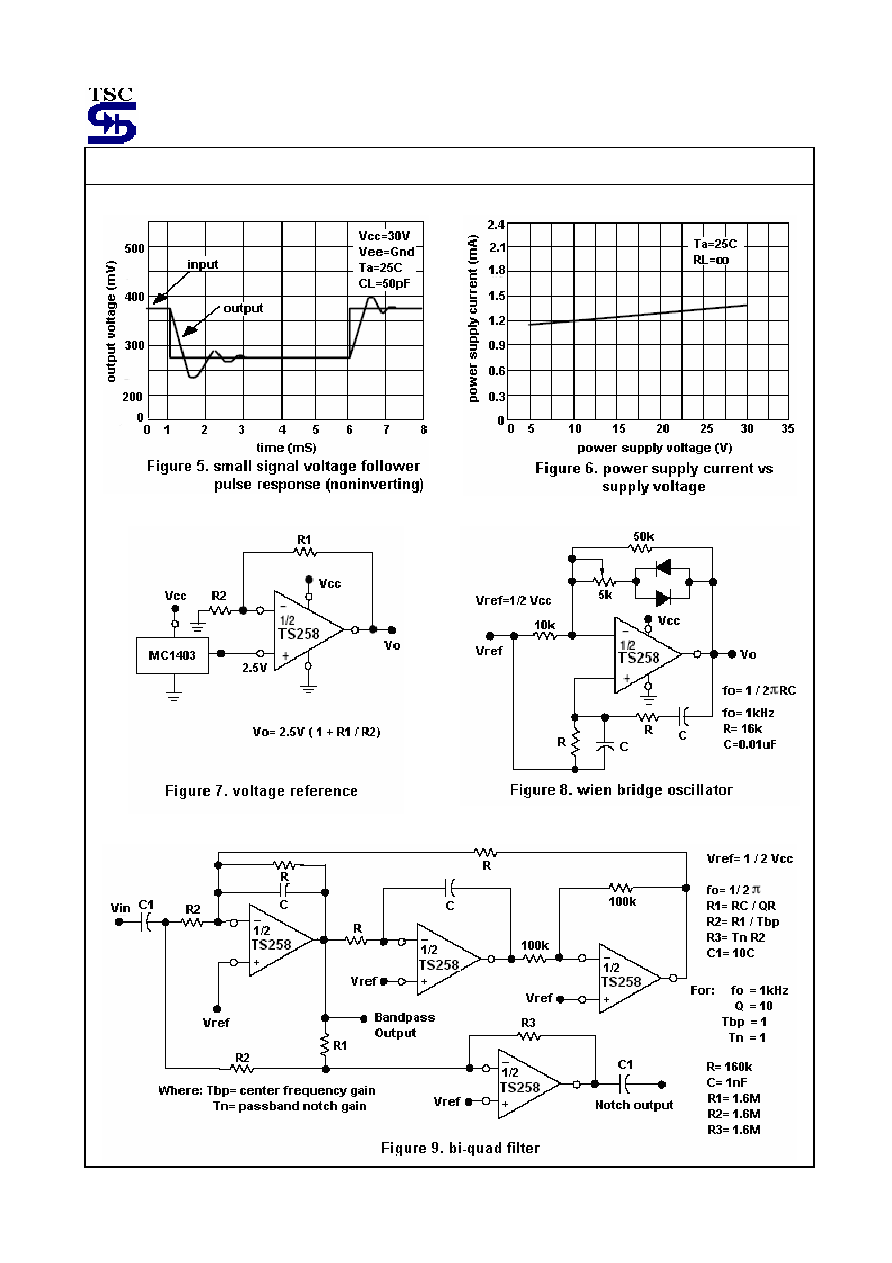
Electrical Characteristics Curve