TS809/810/809R/810R
1-6
2004/09 rev. D
TS809/ 810/ 809R/ 810R
Microprocessor Reset Circuit
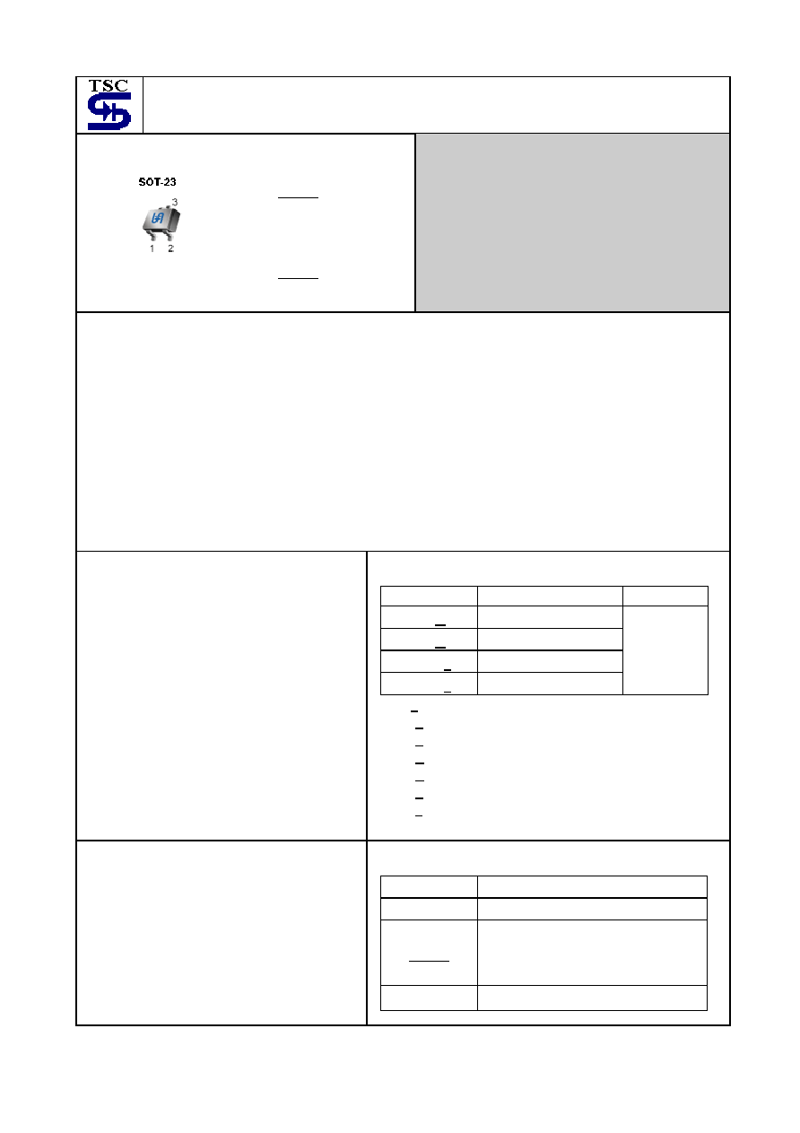
Pin assignment:
TS809/810
1. Gnd
2. RESET (RESET)
3. Vcc
Pin assignment:
TS809R/810R
1.
RESET (RESET)
2.
Gnd
3.
Vcc
Threshold Voltage Option
From 2.63V ~ 4.63V
General Description
The TS809/810/809R/810R are microprocessor (�P) supervisory circuit used to monitor the power supplies in �P and
digital systems. They provide excellent circuit reliability and low cost by eliminating external components and
adjustments when used with +5V, +3.3V, +3.0V powered circuits. These circuits perform a single function: they assert
a reset signal whenever the VCC supply voltage declines below a preset threshold, keeping it asserted for at least
240ms(typ) after VCC has risen above the reset threshold. Reset thresholds suitable for operation with a variety of
supply voltages are available. The TS809/810/809R/810R have push pull outputs. The TS809/809R have an active
low RESET output, while the TS810/810R has an active high RESET output. The reset comparator is designed to
ignore fast transients on VCC, and the output guaranteed to be in the correct logic state for VCC down to 1V. Low
supply correct makes the TS809/810/809R/810R ideal for use in portable equipment.
The TS809/810/809R/810R is available in a 3-pin SOT-23 package.
Features
Precision monitoring of +3V, +3.3V and +5V
power supply voltage
Fully specified over temperature
Available in three output configurations
Push-Pull RESET low output
(TS809 & TS809R)
Push-Pull RESET high output
(TS810 & TS810R)
140mS min. power-on reset pulse width
12uA supply current
Guaranteed reset valid to Vcc = +1V
Power supply transient immunity
No external components
Ordering Information
Note: x is the threshold voltage type, option as
A: 4.63V
B: 4.38V
C: 4.00V
D: 3.08V
E: 2.93V
F: 2.63V
Part No.
Enable Function
Package
TS809CX x Active-Low
TS810CX x Active-High
TS809RCXx Active-Low
TS810RCXx Active-High
SOT-23
Applications
Computers
Controllers
Intelligent instruments
Critical uP and uC power monitoring
Portable / Battery powered equipment
Automotive
Pin Descriptions
Name Description
Gnd Ground
RESET
(RESET)
Reset output pin
L: for TS809 & TS811
H: for TS809R & TS811R
Vcc
Operating voltage input

TS809/810/809R/810R
2-6
2004/09 rev. D
Absolute Maximum Rating
Terminal Voltage (with respect to Gnd)
V
CC
- 0.3 ~ +6.0
V
RESET & (RESET) push-pull
V
RESET
- 0.3 ~ (V
CC
+0.3)
V
Input Current, Vcc
I
CC
20 mA
Output Current, RESET, (RESET)
I
O
20 mA
Continuous Power Dissipation (Ta=+70
o
C)
de-rate 4mW/
o
C above +70
o
C
P
D
320 mW
Operating Junction Temperature Range
T
OP
-40 ~ +105
o
C
Storage Temperature Range
T
STG
-65 ~ +150
o
C
Lead Soldering Temperature (260
o
C) T
LEAD
10 S
Electrical Characteristics
(Ta = 25
o
C, unless otherwise specified.)
Parameter Conditions
Symbol
Min
Typ
Max
Unit
Input Supply Voltage
Ta = 0
o
C ~ +70
o
C V
CC
1.0 -- 5.5 V
V
CC
5.5V
--
19
60
Supply Current
V
CC
3.6V
I
CC
- 17 50
uA
TS809/910/809R/810RCXA 4.56
4.63
4.7
TS809/910/809R/810RCXB
4.31 4.38 4.45
TS809/910/809R/810RCXC
3.94 4.00 4.06
TS809/910/809R/810RCXD
3.03 3.08 3.13
TS809/910/809R/810RCXE
2.89 2.93 2.97
Reset Threshold
TS809/910/809R/810RCXF
V
TH
2.59 2.63 2.67
V
Reset Threshold
Temperature Coefficient
V
TH
-- 30 --
ppm/
o
C
Vcc Rising Time to Function
Ta = -20
o
C ~ +105
o
C
25
--
--
uS/V
V
CC
to Reset Delay
V
CC
= V
TH
to (V
TH
- 100mV)
20
100
uS
Reset Active Timeout Period
Ta = 0
o
C ~ +70
o
C
T
DELAY
100 240 600 mS
V
CC
= V
TH(MIN),
I
SINK
=1.2mA,
TS809 & TS809R
-- -- 0.3
V
CC
= V
TH(MIN),
I
SINK
=3.2mA, --
--
0.4
RESET Output Voltage Low
V
CC
> 1.0V, I
SINK
=50uA
V
OL
-- -- 0.3
V
V
CC
> V
TH(MAX),
I
SOURCE
=500uA,
TS809 & TS809R
0.8 V
CC
-- --
RESET Output Voltage High
V
CC
> V
TH(MAX),
I
SOURCE
=800uA,
V
OH
V
CC �
1.5
-- --
V
V
CC
= V
TH(MAX),
I
SINK
=1.2mA,
TS810 & TS810R
-- -- 0.3
RESET Output Voltage Low
V
CC
= V
TH(MAX),
I
SINK
=3.2mA,
V
OL
-- -- 0.4
V
RESET Output Voltage High
1.8V < V
CC
< V
TH(MIN),
I
SOURCE
=150uA,
TS810 & TS810R
V
OH
0.8
V
CC
-- -- V
TS809/810/809R/810R
3-6
2004/09 rev. D
Application Note
Function Description
A microprocessor's (�P's) reset input starts the �P
In a know state. The TS809/810/809R/810R assert
reset to prevent code-execution errors during power-up,
power-down, or brownout conditions. They assert a
reset signal whenever the Vcc supply voltage declines
below a preset threshold, keeping it asserted for at
least 140ms after Vcc has risen above the reset
threshold. The TS809/810/809R/810R have a push-pull
output stage.
Applications Information
Negative-Going VCC transients in addition to issuing a
reset to the �P during power-up, power-down, and
brownout conditions, the TS809/810/809R/810R are
relatively immune to short-duration negative-going Vcc
transients (glitches).
The TS809/810/809R/810R do not generate a reset
pulse. The graph was generated using a negative going
pulse applied to Vcc, starting 0.5V above the actual
reset threshold and ending below it by the magnitude
indicated (reset comparator overdrive). The graph
indicates the maximum pulse width a negative going
Vcc transient can have without causing a reset pulse.
As the magnitude of the transient increases (goes
farther below the reset threshold), the maximum
allowable pulse width decreases. Typically, a Vcc
transient that goes 100mV below the reset threshold
and lasts 20�S or less will not cause a reset pulse. A
0.1�F bypass capacitor mounted as close as possible
to the Vcc pin provides additional transient immunity.
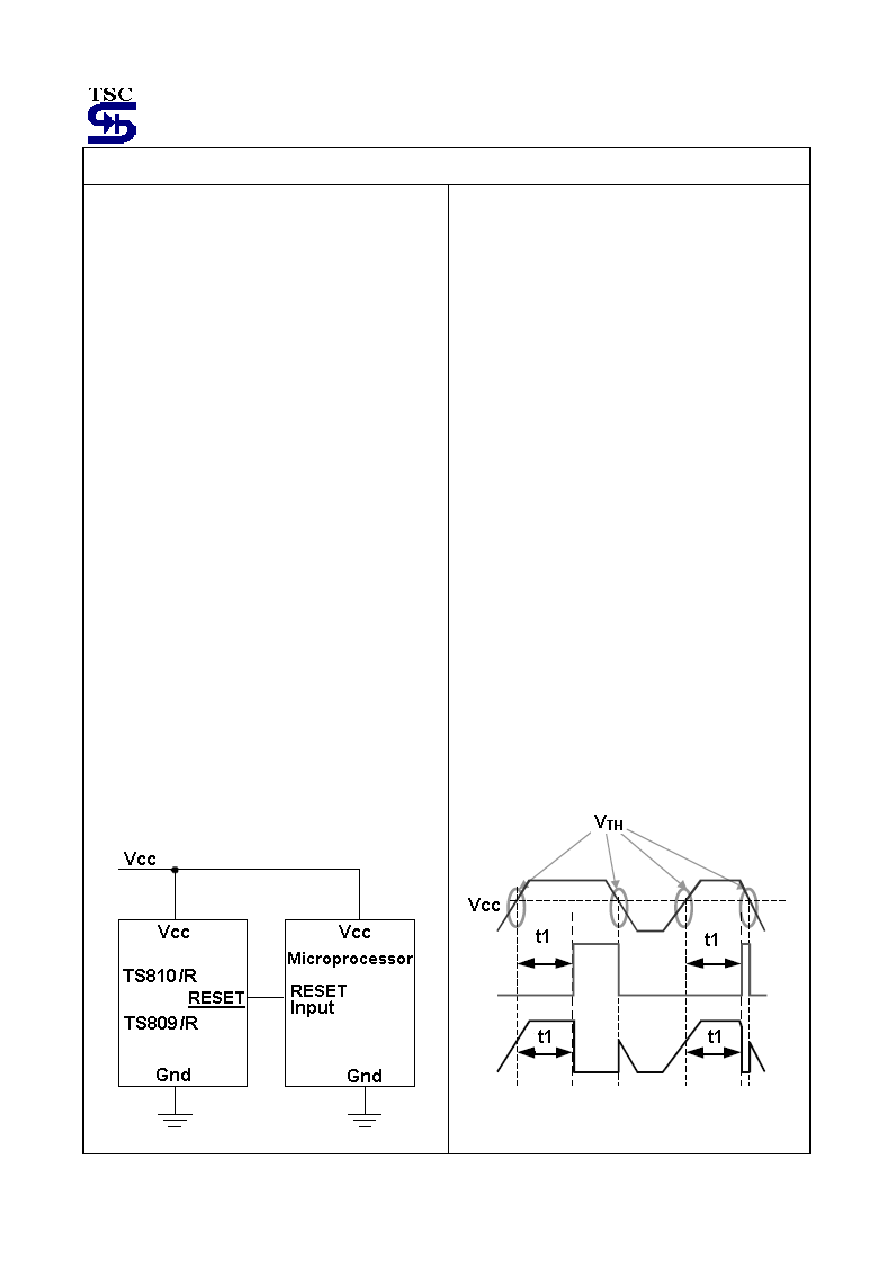
Applications Circuit
Ensuring a Valid Reset Output
Down to Vcc=0
When Vcc falls below 1V, the TS809/810/809R/810R
RESET output no longer sinks current - it becomes an
open circuit. Therefore, high impedance CMOS logic
input connected to RESET can drift to undetermined
voltages.
This present no problem in most applications since
most �P and other circuitry is inoperative with Vcc
below 1V.However, in applications where RESET must
be valid down to 0V, adding a pull down resistor to
RESET causes and stray leakage currents to flow to
ground, holding RESET low (Figure 2.) R1's value is
not critical; 100K is large enough not to load RESET
and small enough to pull RESET to ground. For the
TS809/810/809R/810R if RESET is required to remain
valid for Vcc<1V.
Benefits of Highly Accurate
Reset Threshold
Most �P supervisor ICs have reset threshold voltages
between 5% and 10% below the value of nominal
supply voltages. This ensures a reset will not occur
within 5% of the nominal supply, but will occur when
the supply is 10% below nominal. When using ICs
rated at only the nominal supply �5%, this leaves a
zone of uncertainty where the supply is between 5%
and 10% low, and where the reset many or may not be
asserted.
Timing Diagram

TS809/810/809R/810R
4-6
2004/09 rev. D
Electrical Characteristics Curve
Figure 1. Iq v.s. Temperature
Figure 2. Threshold v.s. Temperature
Figure 3. Immunity
TS809/810/809R/810R
5-6
2004/09 rev. D
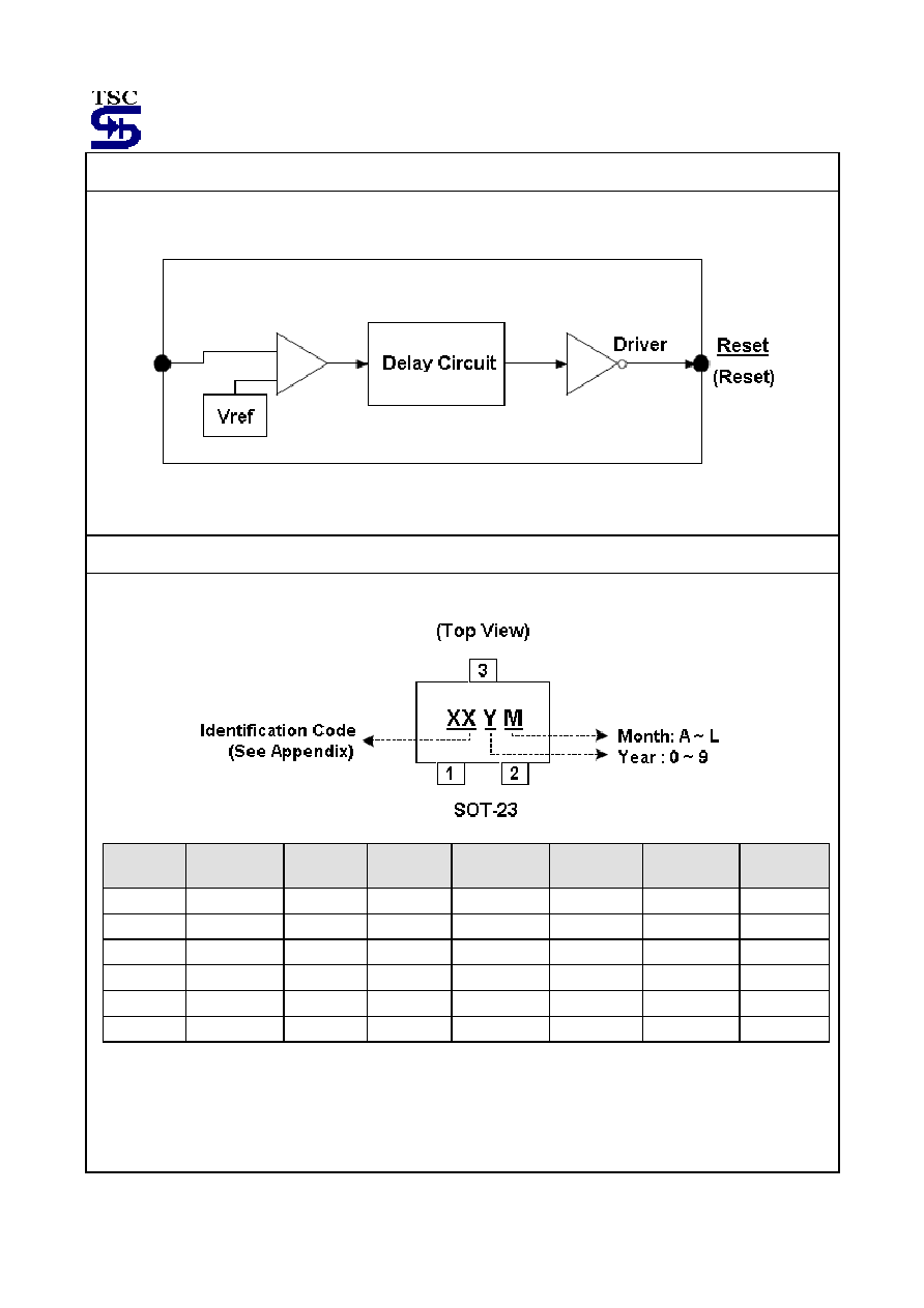
Function Block
Marking Information
Part No.
Identification
Code
Part No. Identification
Code
Part No.
Identification
Code
Part No.
Identification
Code
TS809CXA EA
TS810CXA E0
TS809RCXA EG
TS810RCXA E7
TS809CXB EB
TS810CXB E2
TS809RCXB EH
TS810RCXB E8
TS809CXC EC TS810CXC E3
TS809RCXC EI TS810RCXC E9
TS809CXD ED TS810CXD E4
TS809RCXD EJ
TS810RCXD EM
TS809CXE EE
TS810CXE E5
TS809RCXE EK
TS810RCXE EN
TS809CXF EF
TS810CXF E6
TS809RCXF EL
TS810RCXF EP
TS809/810/809R/810R
6-6
2004/09 rev. D
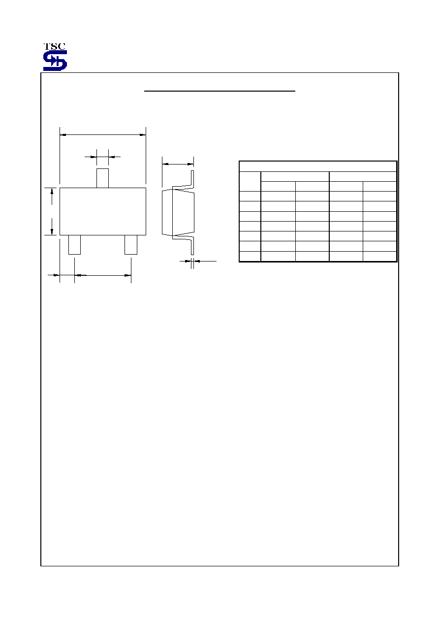
SOT-23 Mechanical Drawing
D
C
A
E
B
G
F
SOT-23 DIMENSION
MILLIMETERS INCHES
DIM
MIN MAX MIN MAX
A 2.88 2.91 0.113 0.115
B 0.39 0.42 0.015 0.017
C 1.78 2.03 0.070 0.080
D 0.51 0.61 0.020 0.024
E 1.59 1.66 0.063 0.065
F 1.04 1.08 0.041 0.043
G 0.07 0.09 0.003 0.004