TS9000/A series
1-4
2003/12 rev. B
TS9000/TS9000A
300mA CMOS Low Dropout Voltage Regulator
General Description
The TS9000/TS9000A series is a positive voltage regulator developed utilizing CMOS technology featured low quiescent
current, low dropout voltage and high output voltage accuracy. Built in low on-resistor provides low dropout voltage and
large output current. A 2.2uF or greater can be used as an output capacitor.
The TS9000/TS9000A series are prevented device failure under the worst operation condition with both thermal
shutdown and current fold-back. These series are recommended for configuring portable devices and large current
application, respectively.
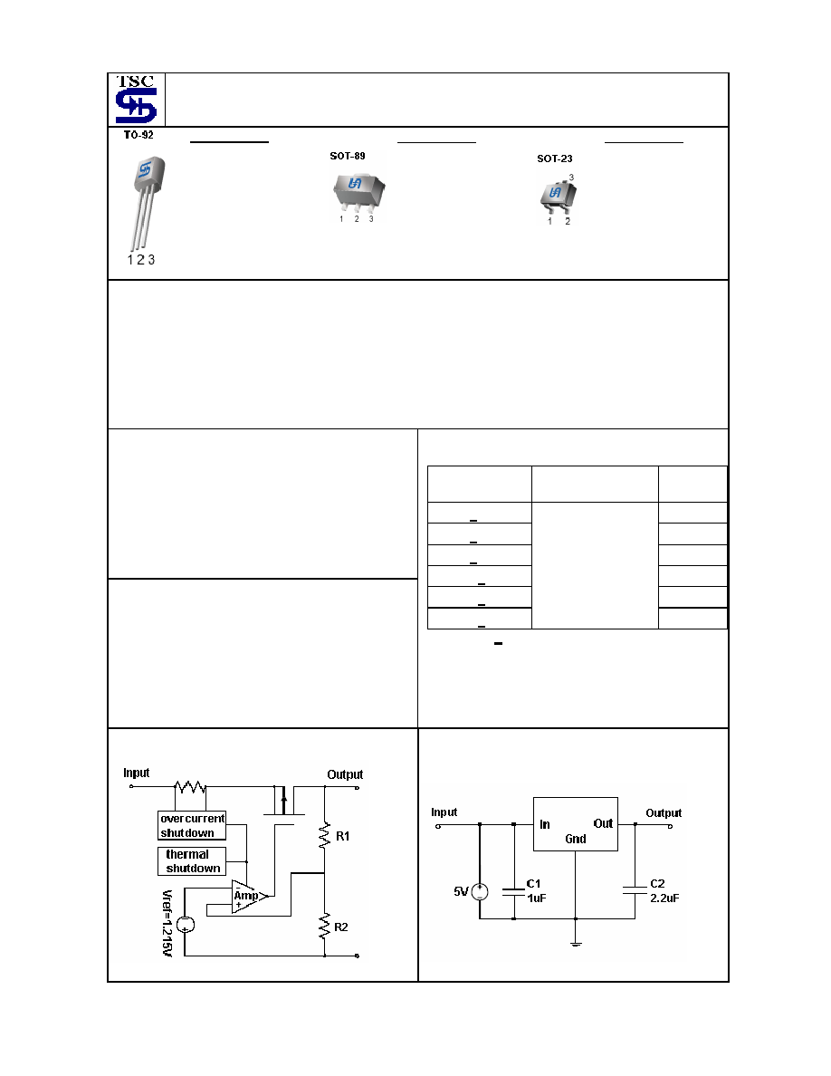
This series are offered in 3-pin TO-92, SOT-89 and SOT-23 package.
Features
Dropout voltage typically 0.4V @Io=300mA
Output current up to 300mA
Low
quiescent
current
Output voltage trimmed before assembly
Internal current limit
Thermal shutdown protection
Applications
Battery power equipment
Personal communication devices
Home
electronic
appliances
PC
peripherals
CD-ROM
Digital signal camera
Ordering Information
Note: Where
x
denotes voltage option, available are
K
=2.5V,
M
=2.7V,
N
=2.8V,
P
=3.0V,
S
=3.3V,
U
=3.5V,
V
=3.6V,
X
=3.8V.
Contact factory for additional voltage options.
Part No.
Operating Temp.
(Ambient)
Package
TS9000
x
CT TO-92
TS9000
x
CX
SOT-23
TS9000
x
CY
SOT-89
TS9000A
x
CT
TO-92
TS9000A
x
CX
SOT-23
TS9000A
x
CY
-40 ~ +85
o
C
SOT-89
Block Diagram
Typical Application Circuit
Pin assignment
TS9000
1. Gnd
2. Input
3. Output
TS9000A
1. Input
2. Gnd
3. Output
Pin assignment
TS9000
1. Gnd
2. Input
3. Output
TS9000A
1. Output
2. Gnd
3. Input
Pin assignment
TS9000
1. Input
2. Output
3. Gnd
TS9000A
1. Gnd
2. Output
3. Input
TS9000/A series
2-4
2003/12 rev. B
Absolute Maximum Rating
Input Supply Voltage
Vin
+7
V
Output Current
Io
P
D
/ (Vin � Vo)
V
Power Dissipation SOT-23
SOT-89
TO-92
P
D
0.3
0.5
0.65
W
Thermal Resistance SOT-23
SOT-89
TO-92
ja
325
180
160
o
C/W
Operating Junction Temperature Range
Tj
-40 ~ +150
o
C
Storage Temperature Range
T
STG
-65 ~ +150
o
C
Lead Soldering Temperature (260
o
C)
10
S
Caution
: Stress above the listed absolute rating may cause permanent damage to the device
.
Electrical Characteristics
Ta = 25
o
C unless otherwise specified.
Parameter Conditions
Min Typ Max
Unit
Output Voltage
Vin=Vo + 0.3V,
1mA
Io
300mA,
0.985|Vo| 1.015|Vo|
Input Supply Voltage
Vo+0.3V
--
7
V
Output Voltage Temperature
Coefficient
-- 40 --
ppm/
o
C
Line Regulation
Vo+1V
Vin Vo+2V,
Io=5mA
-- 0.02 0.1 %
Load Regulation
1mA
I
L
300mA
--
0.2
1.0
%
Dropout Voltage
Io=300mA, Vo=Vo-2%
--
--
400
mV
Quiescent Current
Vin=5V, Io=0A
--
30
50
uA
Short Circuit Current
Vout < 0.4V
--
300
400
mA
Output
Noise
-- 20 --
uVrms
Power Supply Rejection Ratio
At 1KHz
--
55
--
dB
Detail Description
The TS9000/TS9000A series of CMOS regulators contain a P-MOS pass transistor, voltage reference, error amplifier,
over current protection and thermal shutdown.
The TS9000/TS9000A series switches from voltage mode to current mode when the load exceeds the rated output
current. This prevents over stress. The TS9000 also incorporates current fold-back to reduce power dissipation when
the output is short circuit. This feature becomes active when the output drops below 0.8V, and reduces the current flow
by 65%. Full current is restored when the voltage exceeds 0.8V.
The internal P-channel pass transistor receives data from the error amplifier, over current shutdown and thermal
protection circuits. During normal operation, the error amplifier compares the output voltage to a precision reference.
Over current and thermal shutdown circuits become active when the junction temperature exceeds 150
o
C, or the
current exceeds 300mA. During thermal shutdown, the output voltage remains low. Normal operation is restored when
the junction temperature drops below 110
o
C.
TS9000/A series
3-4
2003/12 rev. B
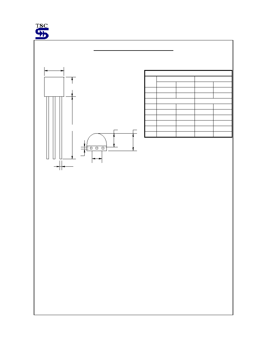
SOT-89 Mechanical Drawing
SOT-89 DIMENSION
MILLIMETERS INCHES
DIM
MIN MAX MIN MAX
A 4.40 4.60 0.173 0.181
B 1.50 1.7 0.059 0.070
C 2.30 2.60 0.090 0.102
D 0.40 0.52 0.016 0.020
E 1.50 1.50 0.059 0.059
F 3.00 3.00 0.118 0.118
G 0.89 1.20 0.035 0.047
H 4.05 4.25 0.159 0.167
I 1.4 1.6 0.055
0.068
J 0.35 0.44 0.014 0.017
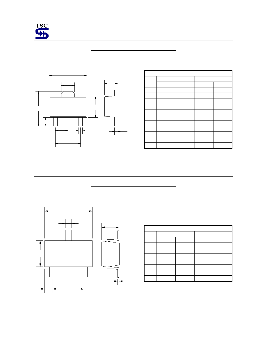
SOT-23 Mechanical Drawing
D
C
A
E
B
G
F
SOT-23 DIMENSION
MILLIMETERS INCHES
DIM
MIN MAX MIN MAX
A 2.88 2.91 0.113 0.115
B 0.39 0.42 0.015 0.017
C 1.78 2.03 0.070 0.080
D 0.51 0.61 0.020 0.024
E 1.50 1.70 0.059 0.067
F 1.04 1.08 0.041 0.043
G 0.07 0.09 0.003 0.004
H
F
E
B
A
G
C
D
J
I