 | ÐлекÑÑоннÑй компоненÑ: TS9010 | СкаÑаÑÑ:  PDF PDF  ZIP ZIP |
Äîêóìåíòàöèÿ è îïèñàíèÿ www.docs.chipfind.ru
TS9010 series
1-4
2004/09 rev. C
TS9010
150mA CMOS Low Dropout Voltage Regulator with Enable
Low Power Consumption
Low Drop Out Voltage 0.4V
Enable Shutdown
General Description
The TS9010 series is combine high accuracy with very low power consumption, providing high output current even when
the application requires very low dropout voltage. The Chip Enable (CE) includes a CMOS or TTL compatible input allows
the output to be turned off to prolong battery life. The TS9010 series is included a precision voltage reference, error
correction circuit, a current limited output driver and over temperature shutdown.
This series are offered in 5-pin SOT-25 package.
Features
Dropout voltage typically 0.4V @Io=150mA (Vo=5V)
Output current up to 150mA (Vout=3V)
Low power consumption
Output voltage +/-2%
Internal current limit
Thermal shutdown protection
Ordering Information
Note: Where
x
denotes voltage option, available are
A
= 1.5V
D
= 1.8V,
K
= 2.5V,
S
= 3.3V,
5
= 5.0V.
Contact factory for additional voltage options.
Part No.
Operating Temp.
(Ambient)
Package
TS9010
x
CX5
-40 ~ +85
o
C SOT-25
Applications
Palmtops
Video
recorders
Battery powered equipment
PC
peripherals
High-efficiency linear power supplies
Digital signal camera
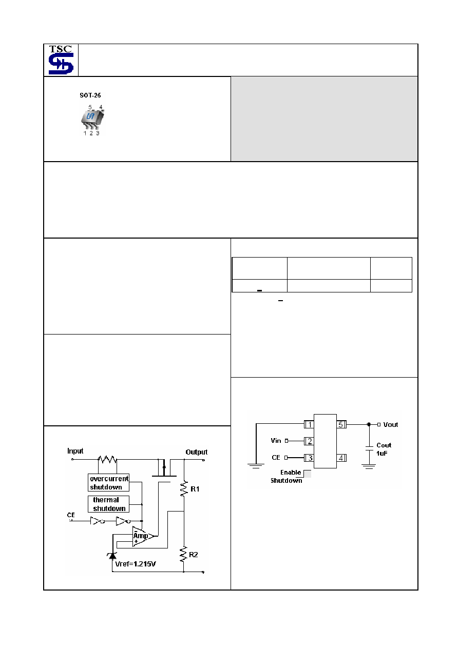
Block Diagram
Typical Application Circuit
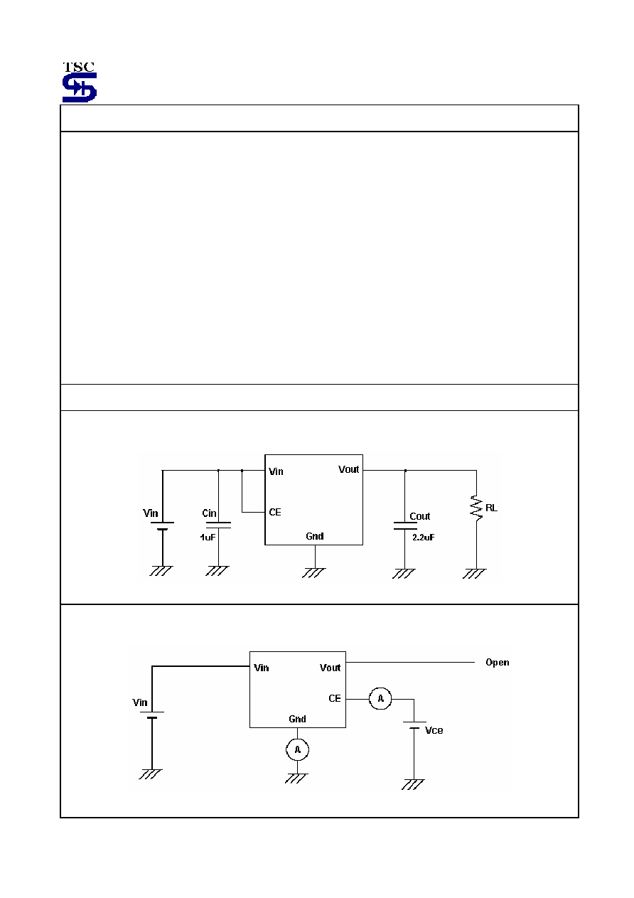
CE (pin 3) may be connected directly to Vin (pin 2)
Pin assignment
1. Ground
2. Input
3. Enable
4. N/C
5. Output
TS9010 series
2-4
2004/09 rev. C
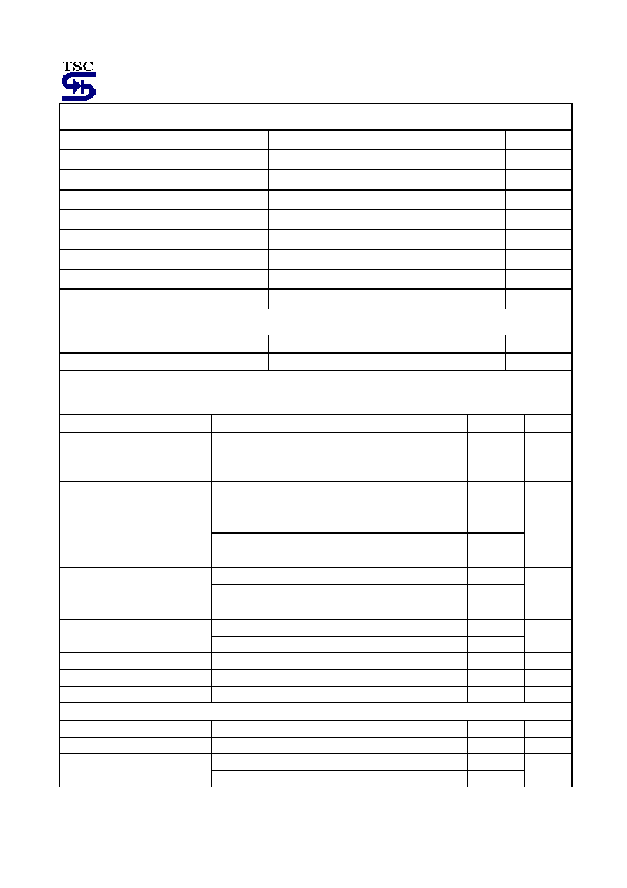
Absolute Maximum Rating
(Note 1)
Description
Symbol
Value
Unit
Input Supply Voltage
Vin
+12
V
Enable Input Voltage
Vce
0 ~ Vin+0.3
V
Output Current
Io
200
mA
Power Dissipation (Note 3)
P
D
380
mW
Thermal Resistance
ja 220
o
C/W
Operating Junction Temperature Range
Tj
-40 ~ +125
o
C
Storage Temperature Range
T
STG
-65 ~ +150
o
C
Lead Soldering Temperature (260
o
C)
5
S
Recommend Operating Rating
(Note 2)
Input Supply Voltage
Vin
+10
V
Enable Input Voltage
Vce
Gnd-0.3 ~ Vin+0.3
V
Electrical Characteristics
Ta = 25
o
C, Cout=2.2uF, Vce2V, unless otherwise specified.
Parameter Conditions
Min
Typ
Max
Unit
Output Voltage
Vin=Vo + 1V, Io= 40mA
0.98|Vo|
1.02|Vo|
V
Output Voltage Temperature
Coefficient (Note 4)
-- 100 --
ppm/
o
C
Line Regulation
Vo+1V
Vin Vo+2V, Io=1mA
--
0.2
0.3
%/V
Vin=Vo+1V,
1mA
I
L
150mA
Vo
2.5V
--
30
80
Load Regulation (Note 5)
Vin=Vo+1V,
1mA
I
L
80mA
Vo< 2.5V
--
40
90
mV
Io=80mA --
200
400
Dropout Voltage (Note 6)
Io=150mA
-- 400 700
mV
Quiescent Current
Vin
0.4V (shutdown)
--
0.01
1
uA
Vin=Ven=Vo+1V --
--
19
Ground Pin Current (Note 7)
Vin=Vo+1V, Ven=Gnd
--
--
0.1
uA
Output Current Limit
Vout=0V
--
300
--
mA
Power Supply Rejection Ratio
At f=100Hz, Io=0.1mA,
--
45
--
dB
Thermal Regulation (Note 8)
--
0.05
--
%/W
Enable Input
Enable Input Logic-Low Voltage
Regulation shutdown
--
--
0.25
V
Enable Input Logic-High Voltage Regulation
enable
1.5
--
--
V
Vce=Vin --
--
1
Enable Input Current
Vce=Gnd 0.2
0.05
0
uA
TS9010 series
3-4
2004/09 rev. C
Electrical Characteristics (continued)
Note 1: Exceeding the absolute maximum rating may damage the device.
Note 2: The device is not guaranteed to function outside its operating rating.
Note 3: The maximum allowable power dissipation at any Ta is Pd(max) = [ Tj(max) - Ta] * ja. Exceeding the
maximum allowable power dissipation will result in excessive die temperature, and the regulator will go into
thermal shutdown.
Note 4: Output voltage temperature coefficient is defined as the worst case voltage change divided by the total
temperature range.
Note 5: Regulation is measured at constant junction temperature using low duty cycle pulse testing. Parts are tested for
load regulation in the load range from 1mA to 150mA(Vout>2.5V) and 1mA to 80mA(Vout<2.5V). Changes in
output voltage due to heating effects are covered by the thermal regulation specification.
Note 6: Dropout voltage is defined as the input to output differential at which the output voltage drops 2% below its
nominal value measured at 1V differential.
Note 7: Ground pin current is the regulator quiescent current plus pass transistor base current. The total current drawn
from the supply is the sum of the load current plus the ground pin current.
Note 8: Thermal regulation is defined as the change in output voltage at a time "t" after a change in power dissipation is
applied, excluding load or line regulation effects. Specifications are for a 150mA load pulse at Vin=12V for
t=10mS.
Application Examples
Standard Circuit
Typical Application Circuit 2
TS9010 series
4-4
2004/09 rev. C
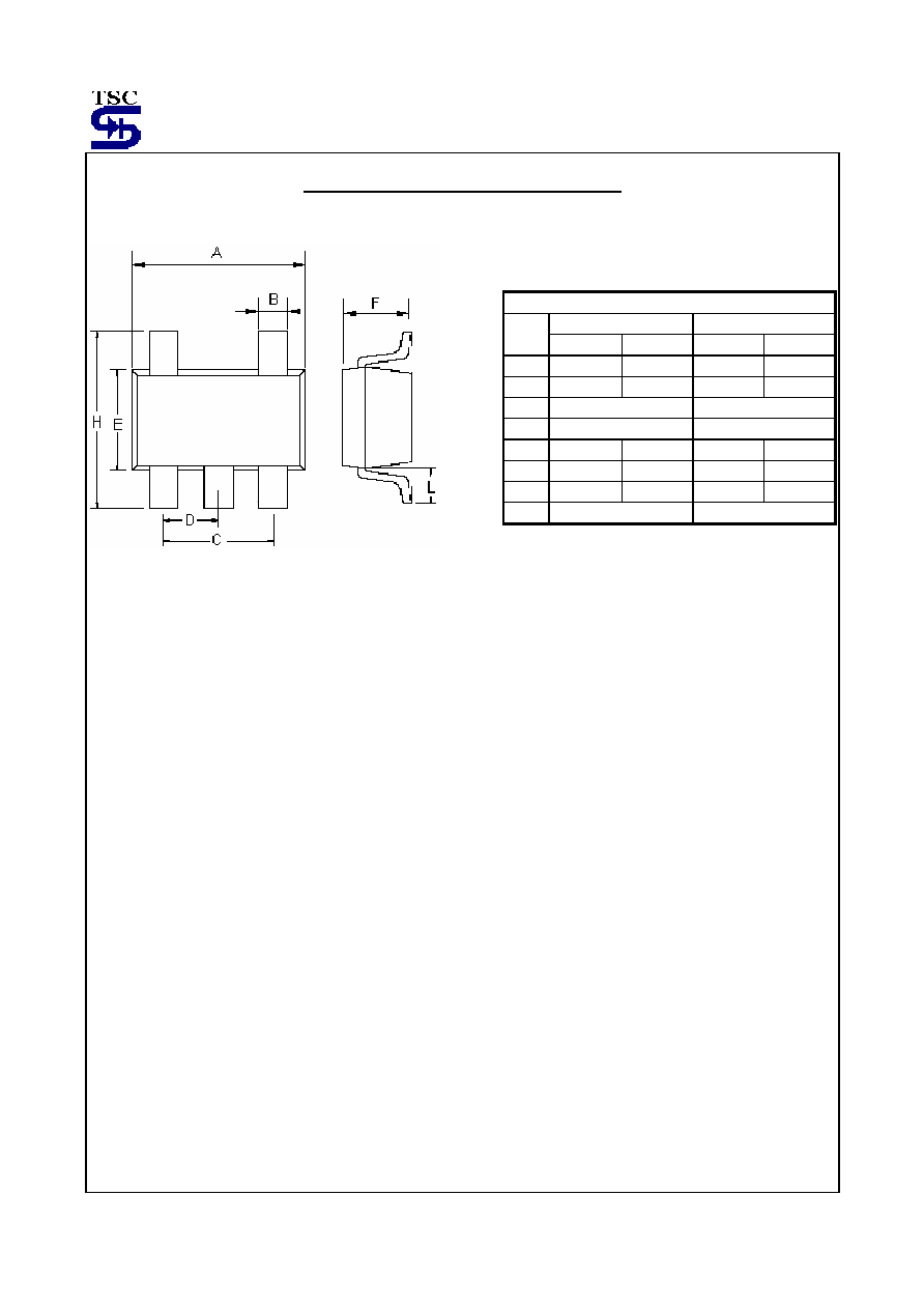
SOT-25 Mechanical Drawing
SOT-23 DIMENSION
MILLIMETERS INCHES
DIM
MIN MAX MIN MAX
A 2.70 3.00 0.106 0.118
B 0.25 0.50 0.010 0.020
C 1.90(typ)
0.075(typ)
D 0.95(typ)
0.037(typ)
E 1.50 1.70 0.059 0.067
F 1.05 1.35 0.041 0.053
H 2.60 3.00 0.102 0.118
L 0.60(typ)
0.024(typ)