LOW VOLTAGE CMOS
256K ELECTRICALLY ERASABLE PROGRAMMABLE ROM
32K X 8 BIT EEPROM
ADDRESSES (A0 - A14)
The Addresses are used to select an 8 bits
memory location during a write or read opera-
tion.
OUTPUT ENABLE (OE)
The Output Enable input activates the output buff-
ers during the read operations.
CHIP ENABLES (CE)
The Chip Enable input must be low to enable all
read/write operation on the device. By setting CE
high, the device is disabled and the power con-
sumption is extremely low with the standby cur-
rent below 35 µA.
FEATURES:
∑
200 ns Access Time
∑
Automatic Page Write Operation
Internal Control Timer
Internal Data and Address Latches for 64 Bytes
∑
Fast Write Cycle Times
Byte or Page Write Cycles: 10 ms
Time to Rewrite Complete Memory: 5 sec
Typical Byte Write Cycle Time: 160 µsec
∑
Software Data Protection
∑
Low Power Dissipation
20 mA Active Current
35 µA CMOS Standby Current
∑
Direct Microprocessor End of Write Detection
Data Polling
∑
High Reliability CMOS Technology with Self Redundant
EEPROM Cell
Typical Endurance: 100,000 Cycles
Data Retention: 10 Years
∑
TTL and CMOS Compatible Inputs and Outputs
∑
Single 3.3 V ± 10% Power Supply for Read and
Programming Operations
∑
JEDEC Approved Byte-Write Pinout
DESCRIPTION:
The Turbo IC 28LV256 is a 32K X 8 EEPROM fabricated
with Turbo's proprietary, high reliability, high performance
CMOS technology. The 256K bits of memory are organized
as 32K by 8 bits. The device offers access time of 200 ns
with power dissipation below 66 mW.
The 28LV256 has a 64-bytes page write operation, enabling
the entire memory to be typically written in less than 5.0
seconds. During a write cycle, the address and 1 to 64 bytes
of data are internally latched, freeing the address and data
bus for other microprocessor operations. The programming
process is automatically controlled by the device using an
internal control timer. Data polling on one or all I/O can be
used to detect the end of a programming cycle. In addition,
the 28LV256 includes an user-optional software data write
mode offering additional protection against unwanted (false)
write. The device utilizes an error protected self redundant
cell for extended data retention and endurance.
WRITE ENABLE (WE)
The Write Enable input initiates the writing of data
into the memory.
DATA INPUT/OUTPUT (I/O0-I/O7)
Data Input/Output pins are used to read data out
of the memory or to write Data into the memory.
PIN DESCRIPTION
Turbo IC, Inc.
28LV256
4
3
5
2
1
6
7
8
9
10
11
12
13
30
31
32
A8
A9
A11
NC
OE
A10
CE
I/O7
I/O6
A6
A5
A4
A3
A2
A1
A0
NC
I/O0
I/O1
I/O2
GND
NC
I/O3
I/O4
I/O5
A12
A7
A14
NC
VCC
WE
A13
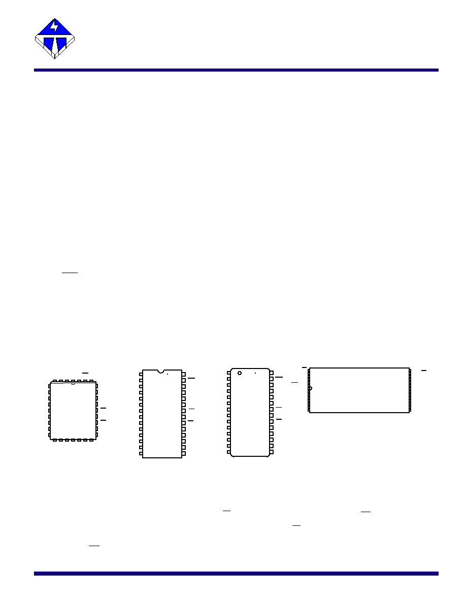
32 pins PLCC
1
2
3
4
5
6
7
8
9
10
11
12
13
14
15
16
17
18
19
20
21
22
23
24
25
26
27
28
A14
A12
A7
A6
A5
A4
A3
A2
A1
A0
I/O0
I/O1
I/O2
GND
VCC
WE
A13
A8
A9
A11
OE
A10
CE
I/O7
I/O6
I/O5
I/O4
I/O3
1
2
3
4
5
6
7
8
9
10
11
12
13
14
15
16
17
18
19
20
21
22
23
24
25
26
27
28
A14
A12
A7
A6
A5
A4
A3
A2
A1
A0
I/O0
I/O1
I/O2
GND
VCC
WE
A13
A8
A9
A11
OE
A10
CE
I/O7
I/O6
I/O5
I/O4
I/O3
1
2
3
4
5
6
7
8
9
10
11
12
13
14
28
27
26
25
24
23
22
21
20
19
18
17
16
15
A10
I/O7
I/O5
I/O3
I/O2
I/O0
A1
A2
A0
I/O1
GND
I/O4
I/O6
CE
OE
A9
A13
VCC
A12
A6
A4
A3
A5
A7
A14
WE
A8
A11
28 pins PDIP
28 pins SOIC (SOG)
28 pins TSOP
14
29
28
27
26
25
24
23
22
21
20
19
18
17
16
15

DEVICE OPERATION
READ:
The 28LV256 is accessed like a static RAM. Read operations are initi-
ated by both CE and OE going low and terminated by either CE or OE
returning high. The outputs are at the high impedance state whenever
CE or OE returns high. The two line control architecture gives designers
flexibility in preventing bus contention.
WRITE:
A write cycle is initiated when CE and WE are low and OE is high. The
address is latched internally on the falling edge of CE or WE whichever
occurs last. The data is latched by the rising edge of CE or WE whichever
occurs first. Once a byte write cycle has been started, the internal timer
automatically generates the write sequence to the completion of the write
operation.
PAGE WRITE OPERATION:
The page write operation of 28LV256 allows one to 64 bytes of data to be
serially loaded into the device and then simultaneously written into memory
during the internally generated write cycle. After the first byte has been
loaded, successive bytes of data may be loaded until the full page of 64
bytes is loaded. Each new byte to be written must be loaded within 200
µs of the previously loaded byte. The page address defined by the ad-
dresses A6-A14 is latched by the first CE or WE falling edge which ini-
tiates a writing cycle and they will stay latched until the completion of the
page write. Any changes in the page addresses during the load-write
cycle will not affect the initially latched page addresses. Addresses A0 -
A5 are used to define which bytes will be loaded and written within the 64
bytes page. The bytes may be loaded in any order that is convenient to
the user. The content of a loaded byte may be altered at any time during
the loading cycle if the maximum allowed byte-load time (200 µs) is not
exceeded. Only loaded bytes within the page will be written; no rewriting
will occur to the non-selected bytes in the page.
DATA POLLING:
The 28LV256 features DATA POLLING to indicate the completion of a
write cycle to the host system. During a byte or page write cycle, an
attempted read of the last byte loaded into the page will result in the
complement of the loaded byte on all outputs I/O0 - I/O7 (i.e. loaded data
01010110, read data 10101001). Data Polling feature may be used by an
attempted read on one or more outputs (whatever is convenient for the
system developer). Once the write cycle has been completed, true data
is valid on all outputs and the next cycle may be started.
DATA PROTECTION:
The 28LV256 has three hardware features to protect the written content
of the memory against inadvertent writes :
a.)
Vcc threshold detector: If Vcc is below 2.5 V, the write capa-
bilities of the chip is inhibited for whatever input conditions.
b.)
Noise protection: A WE, OE, or CE pulse less than 10 ns in
width is not able to initiate a write cycle.
c.)
Write inhibit: Holding OE at low, or CE at high, or WE at high
inhibits the write cycle.
SOFTWARE WRITE PROTECTION:
The 28LV256 offers a software controlled data write protection feature.
The device is delivered to the user with the software data write protection
DISABLED; i.e. the device will go to the data write operation as long as
Vcc exceeds 2.5 V and CE, WE, and OE inputs are set at write mode
levels. The 28LV256 can be automatically protected against an accidental
write operation during power-up or power-down without any external cir-
cuitry by enabling the software data write protection features. This features
is enabled after the first write cycle which includes the software algorithm.
After this operation is done, the data write function of the device may be
performed only if every page write cycle is preceded by the software algo-
rithm. The device will maintain its software protect feature for the rest of its
life unless that the software algorithm for disabling the protection is imple-
mented.
SOFTWARE ALGORITHM:
The 28LV256 has an internal register for the software algorithm which en-
ables the memory to provide the user with additional features:
a.) Software Write Protect Enable
A sequence of three dummy data writes to the memory will activate
internal EEPROM fuses during the first page write cycle. These EE-
PROM fuses will reject any write attempts of new pages of data
unless the three dummy data writes are repeated at the beginning of
any page writes. The timing for the dummy data and addresses must
be the same as for a normal write operation. A violation of the three
steps write protect sequence in data or address timing and content
will abort the procedure and reset the device to the starting point
condition.
Note: After the three dummy data writes, at least one page load/
write cycle must be performed. If no additional page data is added
to the three dummy data writes, the software write protect will
not be enabled until the next write, which will not be protected.
Table 1 shows the required procedure for enabling the software write
protect:
Step
Mode
Address A14-A0
Data I/O 7-0
1
Page Write
5555 Hex
AA Hex
2
Page Write
2AAA Hex
55 Hex
3
Page Write
5555 Hex
A0 Hex
4-67
Page Write
Address
Data
b.) Software Write Protect Disable
The software algorithm of 28LV256 includes a six steps sequence of
dummy data writing to disable the software write protect feature de-
scribed in a.). The six steps write sequence shown in Table 2 must
be performed at the beginning of a page write cycle. A violation of
the six steps write sequence in data or address timing and content
will abort the procedure and reset the chip to the starting point con-
dition. After a page write cycle including the six steps write sequence
has been performed, the 28LV256 does not require the use of three
dummy data writes described in a.) for the following page write cycle.
The device is at the software write protect disabled state.
Note: After the six dummy data writes, at least one page load/
write cycle must be performed. If no additional page data is added
to the six dummy data writes, the software write protect disable
will not be activated. Table 2 shows the required procedure for dis-
abling the software write protect:
Step
Mode
Address A14-A0
Data I/O 7-0
1
Page Write
5555 Hex
AA Hex
2
Page Write
2AAA Hex
55 Hex
3
Page Write
5555 Hex
80 Hex
4
Page Write
5555 Hex
AA Hex
5
Page Write
2AAA Hex
55 Hex
6
Page Write
5555 Hex
20 Hex
7-70
Page Write
Address
Data
c.) Software Chip Clear
The software algorithm of 28LV256 includes a sequence of six steps
dummy data writing to perform a chip clear operation. Table 3 shows
the six steps write sequence to perform the software chip clear op-
eration:
Step
Mode
Address A14-A0
Data I/O 7-0
1
Page Write
5555 Hex
AA Hex
2
Page Write
2AAA Hex
55 Hex
3
Page Write
5555 Hex
80 Hex
4
Page Write
5555 Hex
AA Hex
5
Page Write
2AAA Hex
55 Hex
6
Page Write
5555 Hex
10 Hex
At the end of the six steps write sequence shown in Table 3, the
device automatically activates its internal timer to control the chip
Turbo IC, Inc.
28LV256

erase cycle; typically takes 20 msec. After a software chip clear op-
eration has been completed, all 256K bit locations of memory show
high level at read operation mode.
d.) Software Autoclear Disable Mode
This software algorithm disables the internal automatic clear before
write cycle. Table 4 shows the six steps needed to perform the auto-
clear disable mode:
Step
Mode
Address A14-A0
Data I/O 7-0
1
Page Write
5555 Hex
AA Hex
2
Page Write
2AAA Hex
55 Hex
3
Page Write
5555 Hex
80 Hex
4
Page Write
5555 Hex
AA Hex
5
Page Write
2AAA Hex
55 Hex
6
Page Write
5555 Hex
40 Hex
7-70
Page Write
Address
Data
Page write operation using the software autoclear disable mode will
reduce programming time to typically 5 msec. The page write using
software autoclear disable mode is usually used after a chip clear or
a software chip clear operation. At the end of the six steps sequence,
the autoclear before write is disabled and will stay that way unless a
power-down occurs or the software autoclear enable procedure is
initiated.
e.) Software Autoclear Enable Mode
Automatic page clear before page write can be restored to 28LV256
either by Vcc power-down or by software autoclear enable mode.
Table 5 shows the six steps page write procedure needed to enable
software autoclear mode:
Step
Mode
Address A14-A0
Data I/O 7-0
1
Page Write
5555 Hex
AA Hex
2
Page Write
2AAA Hex
55 Hex
3
Page Write
5555 Hex
80 Hex
4
Page Write
5555 Hex
AA Hex
5
Page Write
2AAA Hex
55 Hex
6
Page Write
5555 Hex
50 Hex
7-70
Page Write
Address
Data
Symbol Parameter
Condition
Min
Max Units
Icc
Active Vcc
CE=OE=Vil; All I/O
20 (C)
mA
Current
Open, Min Read or
30 (I)
mA
Write Cycle Time
50 (M)
mA
Isb1
CMOS
CE=Vcc-0.3 V to
35 (C)
µA
Standby
Vcc+1 V
50 (I&M) µA
Current
Iil
Input
1
µA
Leakage
Current
Iol
Output
10
µA
Leakage
Current
Vil
Input Low
-0.1
-0.6
V
Voltage
Vih
Input High
1.8 Vcc+0.3
V
Voltage
Vol
Output Low
Iol=1.6 mA
0.3
V
Voltage
Voh
Output High
Ioh=-0.1 mA
1.8
V
Voltage
D.C. CHARACTERISTICS
(C) = COMMERCIAL
(I)
= INDUSTRIAL
(M) = MILITARY
Turbo IC, Inc.
28LV256
ABSOLUTE MAXIMUM STRESS RANGES *
TEMPERATURE
Storage:
-65∞
C to 150∞ C
Under Bias:
-55∞ C to 125∞ C
ALL INPUT OR OUTPUT VOLTAGES
with respect to Vss
+6 V to -0.3 V
"Absolute Maximum Ratings" may cause perma-
nent damage to the device. This is a stress rating
only and functional operation of the device at
these or any other conditions above those indi-
cated in the operation section of this specifica-
tion is not implied. Exposure to absolute maxi-
mum rating conditions for extended periods may
affect device reliability.
RECOMMENDED OPERATING CONDITIONS
Temperature Range:
Commercial:
0
∞
C to 70
∞
C
Industrial:
-40
∞
C to 85
∞
C
Military:
-55
∞
C to 125
∞
C
Vcc Supply Voltage:
3.3 V
±
10%
Endurance:
100,000 Cycles/Byte (Typical)
Data Retention:
10 Years
A.C. CHARACTERISTICS - READ OPERATION
28LV256-3
28LV256-4
28LV256-5
28LV256-6
Symbol
Parameters
Min Max Min Max Min Max Min MaxUnit
tacc
Address to
200
250
300
400 ns
Output Delay
tce
CE to Output
200
250
300
400 ns
Delay
toe
OE to Output
110
150
150
150 ns
tdf
OE to Output
0
90
0
90
0
90
0
90 ns
In High Z
toh
Output Hold
0
0
0
0
ns
from Address
Changes, Chip
Enable or
Output Enable
Whichever
Occurs First
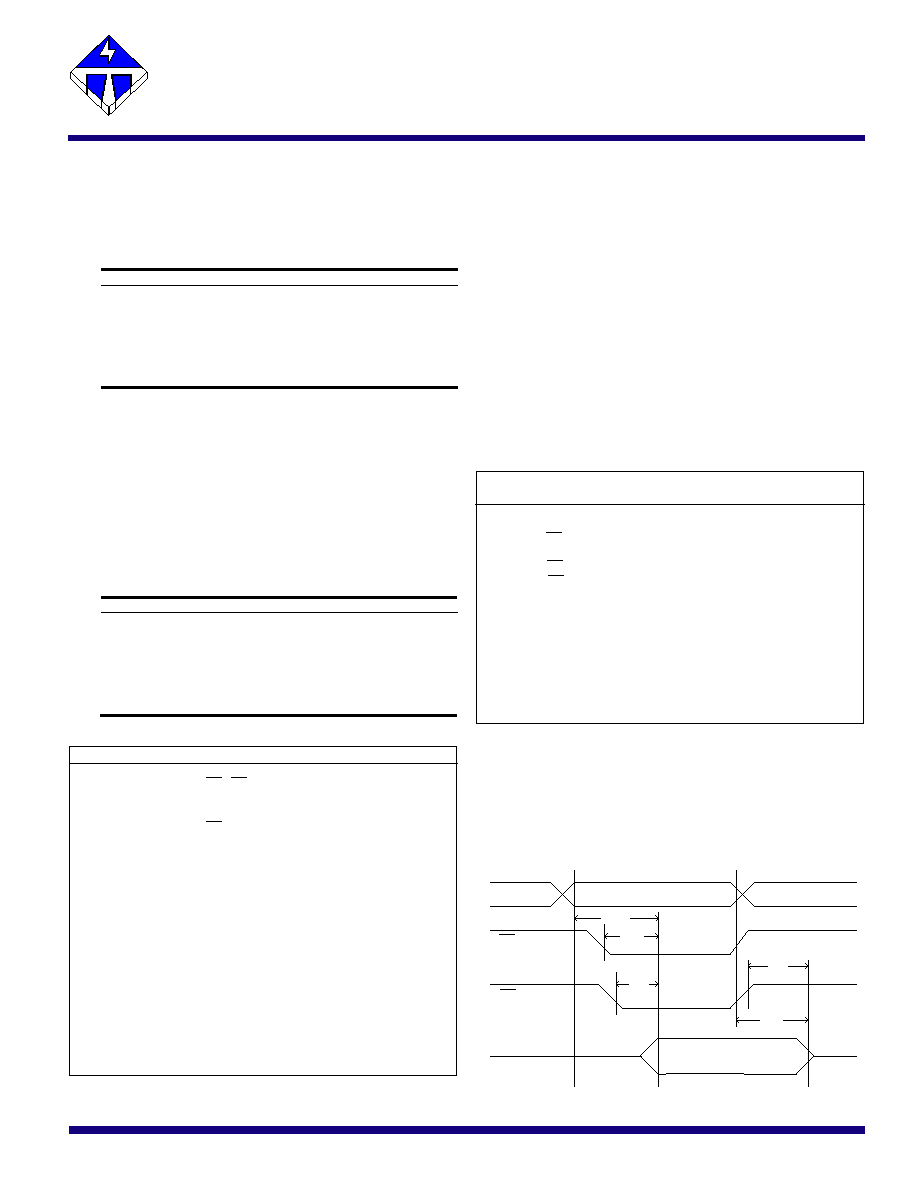
A.C. Read Wave Forms
A.C. TEST CONDITIONS
Output Load : 1 TTL Load and Cl=100 pF
Input Rise and Fall Times : < 10 ns
Input Pulse Level : 0 V to 3 V
Timing Measurement Reference Level : 1.5 V
tacc
ADDRESS VALID
ADDRESS
CE
OE
OUTPUT
HIGH-Z
toe
tce
tdf
toh
OUTPUT VALID
HIGH-Z

TURBO IC PRODUCTS AND DOCUMENTS
1.
All documents are subject to change without notice. Please contact Turbo IC for the latest
revision of documents.
2.
Turbo IC does not assume any responsibility for any damage to the user that may result from
accidents or operation under abnormal conditions.
3.
Turbo IC does not assume any responsibility for the use of any circuitry other than what
embodied in a Turbo IC product. No other circuits, patents, licenses are implied.
4.
Turbo IC products are not authorized for use in life support systems or other critical systems
where component failure may endanger life. System designers should design with error
detection and correction, redundancy and back-up features.
A.C. WRITE CHARACTERISTICS
Symbol Parameter
Min
Max
Units
tas
Address Set-up Time
20
ns
tah
Address Hold Time
100
ns
tcs
Write Set-up Time
0
ns
tch
Write Hold Time
0
ns
tcw
CE Pulse Width
150
ns
twp
WE Pulse Width
150
ns
toes
OE Set-up Time
20
ns
toeh
OE Hold Time
20
ns
tds
Data Set-up Time
50
ns
tdh
Data Hold Time
10
ns
tblc
Byte Load Cycle
0.2
200
µs
tlp
Last Byte Loaded to Data
Polling Output
500
µs
twc
Write Cycle Time
10
ms
twc
Write Cycle Time (IND & MIL)
15
ms
Part Numbers & Order Information
28LV256PC-4
Speed
-3 200 ns
-4 250 ns
-5 300 ns
-6 400 ns
Temperature
C
-Commercial
I
-Industrial
M
-Military
Package
J -PLCC
P -PDIP
S -SOIC
T -TSOP
Turbo IC, Inc. 2365 Paragon Drive, Suite I, San Jose, CA 95131 Phone: 408-392-0208 Fax: 408-392-0207
See us at www.turbo-ic.com
32K x 8
EEPROM
Page Mode Write Wave Form
PAGE MODE WRITE CHARACTERISTICS
Symbol Parameter
Min
Max
Unit
twc
Write Cycle Time
10
ms
tas
Address Set-up Time
20
ns
tah
Address Hold Time
100
ns
tds
Data Set-up Time
50
ns
tdh
Data Hold Time
0
ns
twp
Write Pulse Width
150
ns
tblc
Byte Load Cycle Time
0.2
200
µs
Chip Clear Wave Form
The content of the 28LV256 may be altered to HIGH by the use of the
Chip Clear operation. By setting CE to low, OE to 12 volts, and WE to
low, the entire memory can be cleared (written HIGH) within 20 ms. The
Chip Clear operation is a latch operation mode. After the Chip Clear
starts, the internal chip timer takes over and completes the clear with-
out CE, OE and WE being held active.
A.C. Write Characteristics CE-Controlled
A.C. Write Characteristics WE-Controlled
OE
ADDRESS
CE
WE
DATA
toes
tas
tcs
tah
toeh
tch
twp
tds
tblc
twc
tdh
HIGH-Z
DATA VALID
HIGH-Z
VALID
OE
ADDRESS
CE
WE
DATA
toes
tas
tcs
tah
toeh
tch
twp
tds
tblc
twc
tdh
HIGH-Z
DATA VALID
HIGH-Z
VALID
OE
CE
WE
A0-A5
DATA
twp
tblc
tah
tas
tds
tdh
BYTE-0
BYTE-1
BYTE-2
AD-VALID
AD-VALID
AD-VALID
OE
CE
WE
ts= 20 ns
tp= 200 ns
th= 20 ns
VH=12.0 V±0.5V
tp
th
VH
VIH
VIH
VIL
VIH
VIL
ts
Turbo IC, Inc.
28LV256
Rev. 3.0 - 10/28/01


