
Single-Chip CMOS construction
Single-Chip
selected by jump wire
Wide operating voltage range : V
DO
= 3 to 12 Volts
. Built-in RC oscillator
use 5 % resistor)
n
E a s y
with RF,
and
transmission media
n
Tri-state(0, 1, open) address codes, some of address
The UM3758 series are
programmable
i n C M O S s t r u c t u r e f o r l o w
power
They are enhanced for new
encoder/decoder
to provide many more combinations
for
security.
Most
are achieved by
ing 3 =
combinations. Some
of this
s e r i e s p r o v i d e 4 t o 8 d a t a b i t s f o r c o n t r o l l i n g .
codes used as data
or as internal addresses
by mask
Internal address
is
ie 3
387,428, 489
different
at most
Decoder has
latch data
Series for various applications
n
pin outcompatibleto UM3750
According to the following information, The
n a l a d d r e s s b i i s , 1 8
and 12
be assigned by customer in
for
and confidentialii. Whenever
t h e a d d r e s s
of
t r a n s m i t s , t h e
will check the address codes with his own and
the successive two
address codes will generate
a low pulse. there were any data bits, the
will latch these data bis at the corresponding pins
for controlling.

U M 3 7 5 8 S e r i e s
Power Supply Voltage . . . . . . . . .
to
Operating Temperature . . . . . . . .
to
Storage Temperature (Tstg) . . . . .
to 150�C
Apply Voltage on any Pin . . . . . . . . . . . . . .
0.3
+ 0.3
Stresses above those listed
"Absolute Maximum
Ratings' may
permanent darnage to the device.
These are stress ratings only.
Operation of
this device at these or any other conditions above
those indicated in the operational
of this
specification is not
and exposure to absolute
( T
A
= 25�C ,
= 9 Volts ,
= OV unless otherwise specified)
Parameter
Operating voltage
Operating current
Schmitt Trigger input
level
Other pins input
level
Output pin
level
DATA output current
HIGH level
LOW level
Symbol
Min.
3.0
Vsh
6
Vih
8.5
Vil
0
Voh
8.5
Vol
0
lohd
9
lold
9
T
YP
.
Max.
12
1.2
2
9
0.5
9
1
Unit
V
mA
V
V
V
v
V
v
mA
mA
Conditions
HIGH
HIGH
HIGH
V
DD
= 12V
Voh = 6V
Vol = 6V

S e r i e s
Parameter
Symbol
Min.
Max.
Unit ,
Conditions
HIGH
LOW
loht
35
mA
15
mA
=
Voh 6V
Vol = 6V
Operating frequency
F
160
KHz
+ 15%
of external
Pin Number
UM3758 UM3758
1
2
1
3
2
4
3
5
4
6
5
7
8
6
9
7
10
8
11
UM3758
Designation
Descripti.on
Al
Address select line is tri-state indicated as 0, 1
and open
1
A2
Address select line 2 is tri-state indicated as 0, 1
and open
2
A3
Address select line 3 tri-state indicated as 0, 1
and open
3
A4
Address select line 4 is tri-state
indicated
as 0,
1
and open
4
Address select line 5 is tri-state
indicated
as 0,
1
and open
5
A6
Address select line 6 is tri-state
indicated
as 0,
1
and open
A7
Address select line 7
is tri-state
indicated
as 0,
1
and open
6
A8
Address select line 8 is tri-state
indicated
as 0,
1
and open
and open
Address select line 9 is tri-state indicated as 0, 1
Address select line 10 is tri-state indicated as 0, 1
and open
Address select line 11 is tri-state indicated as 0, 1
and open
U M 3 7 5 8
Pin Number
UM3758 UM3758 UM3758
-12OA
12
9
9
Designation
A l 2
Description
Address select
12 is tri-state indicated as 0, 1
and open
10
NC
11
NC
13
A l 3
No connection
Noconnection
Address select line 13 is tri-state indicated as 0, 1
and open
14
A l 4
Address select line 14 is tri-state indicated as 0, 1
and open
10
12
A l 5
Address select line 15 is tri-state indicated as 0, 1
and open
16
11
13
A l 6
Address select line 16 is tri-state indicated as 0, 1
and open
17
12
14
A l 7
Address select line 17 is tri-state indicated as 0, 1
and open
16
Address select
16 is tri-state indicated as 0, 1
and open
19
13
15
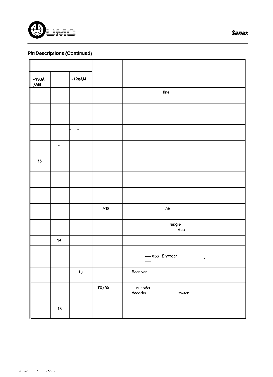
o s c
R.C. input pin for
pin oscillator. A resistor is
connected from this pin to
and a capacitor to Vss
20
16
vss
21
15
17
MODE
The ground pin for UM3756
This pin is used to select transmit or receive mode
MODE
:
mode
MODE
Vss : Decoder mode
22
16
RXINP
input pin. Receives waveform from the detect
circuit
23
17
19
OUT
In
mode, this pin will transmit waveform; in
mode, this pin will
to
LOW
if comparison
is OK
24
20
VDD
The positive power supply of UM3756
4

U M 3 7 5 8 S e r i e s
1
5
6
7
a
9
10
11
12
D
e
s
i
g
n
a
t
i
o
n
Description
a
Al0
9
9
Address select line 1 is tri-state indicated as 0, 1
and open
Address select line 2 is tri-state indicated as 0, 1
and open
Address select line 3 is tri-state indicated as 0, 1
and open
Address select line 4 is tri-state indicated as 0, 1
and open
Address select line 5 is tri-state indicated as 0, 1
and open
A d d r e s s
line 6 is triistate indicated as 0, 1
and open
Address select line 7 tri-state indicated as 0, 1
and open
Address select line 8 is tri-state indicated as 0, 1
and open
A d d r e s s
line 9 is tri-state indicated as 0, 1
and open
Address select line 10 is tri-state indicated as
and open
Data output pin 1, states are either HIGH (1
open)
or LOW (0)
Data output pin 2, states are either HIGH (1 or open)
or LOW (0)