
CHA1077
Ref. DSCHA10773155 - 04 jun 03
1/6
Specifications subject to change without notice
United Monolithic Semiconductors S.A.S.
Route DÈpartementale 128 - B.P.46 - 91401 Orsay Cedex France
Tel. : +33 (0)1 69 33 03 08 - Fax : +33 (0)1 69 33 03 09
PRELIMINARY
W-band Low Noise Amplifier
GaAs Monolithic Microwave IC
Description
The CHA1077 is a W-band monolithic 3-stages
low noise amplifier. All the active devices are
internally self-biased. This chip is compatible
with automatic equipment for assembly.
The circuit is manufactured on P-HEMT
process: 0.15µm gate length, via holes through
the substrate, air bridges and electron beam
gate lithography.
It is available in chip form.
Main Features
n
W-band low noise amplifier
n
High gain
n
Wide operating frequency range
n
High temperature range
n
On-chip self biasing
n
Automatic assembly oriented
n
Low DC power consumption
n
Chip size: 2.6x1.32x 0.1mm
OUT
IN
+V
-V
W-band amplifier block-diagram
Main Characteristics
Tamb = +25∞C
Symbol Parameter Min
Typ
Max
Unit
F_op
Operating frequency
76
77
GHz
G_lin
Small signal gain
15
dB
NF Noise
figure
4.5 dB
P_1dB
Output power at 1dB
10
dBm
ESD Protections : Electrostatic discharge sensitive device observe handling precautions !
CHA1077
W-band LNA
Ref. DSCHA10773155 - 04 jun 03
2/6
Specifications subject to change without notice
Route DÈpartementale 128 , B.P.46 - 91401 ORSAY Cedex - FRANCE
Tel.: +33 (0)1 69 33 03 08 - Fax : +33 (0)1 69 33 03 09
Electrical Characteristics
Full operating temperature range, used according to section "Typical assembly and bias
configuration".
Symbol Parameter
Min
Typ
Max
Unit
F_op
Operating frequency
76
77
GHz
G_lin
Small signal gain
11
15
19
dB
G_fl
Small signal gain flatness
0.5
1
dB
NF
Noise figure
4.5
6.5
dB
P_out_1dB
Output power at 1dB
6.5
10
dBm
Is
Reverse isolation
20
30
dB
VSWR_in
VSWR at input port (50
)
2:1
2.5:1
VSWR_out
VSWR at output port (50
)
2:1
2.5:1
+V
Positive supply voltage (1)
4.4
4.5
4.6
V
+I
Positive supply current
40
70
mA
-V
Negative supply voltage (1)
-4.6
-4.5
-4.4
V
-I
Negative supply current
6
10
mA
Top
Operating temperature range
-40
100
∞C
(1) Negative supply voltage must be applied at least 1us before positive supply
voltage.
Absolute Maximum Ratings (1)
Symbol Parameter
Values
Unit
P_in
Maximum input power (2)
3
dBm
+V
Positive supply voltage
5
V
-V
Negative supply voltage
-5
V
+I
Positive supply current
80
mA
-I
Negative supply current
13
mA
Tstg
Storage temperature range
-55 to +155
∞C
(1)
Operation of this device above anyone of these parameters may cause permanent damage.
(2) CW
mode
W-band LNA
CHA1077
Ref. DSCHA10773155 - 04 jun 03
3/6
Specifications subject to change without notice
Route DÈpartementale 128 , B.P.46 - 91401 ORSAY Cedex - FRANCE
Tel.: +33 (0)1 69 33 03 08 - Fax : +33 (0)1 69 33 03 09
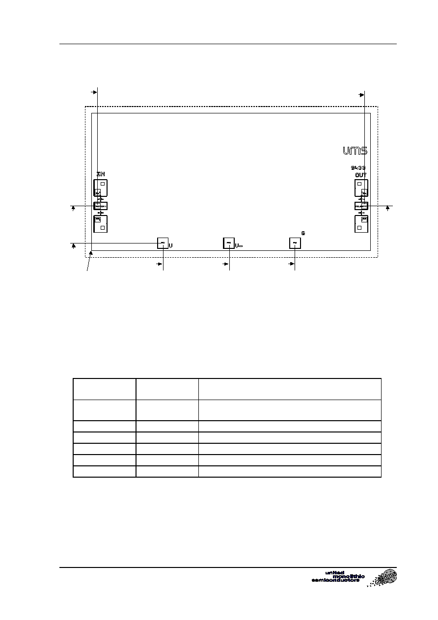
Chip Mechanical Data and Pin References
Origin 0,0
Layout 2530X1250
40
5
55
7
8
9
1
2
3
6
5
4
645
1845
1245
70
2475
40
5
Unit = µm
External chip size (layout size + dicing streets) = 2600X1320 +/-35
Chip thickness = 100 +/- 10
HF Pads (5,8) = 68 x 118
DC/IF Pads = 100 x 100
Pin number
Pin name
Description
4, 6, 7, 9
Ground: should not be bonded. If required,
please ask for more information.
3
Ground (optional)
5
OUT
RF output port
8
IN
RF input port
1
+V
Positive supply voltage
2
-V
Negative supply voltage

CHA1077
W-band LNA
Ref. DSCHA10773155 - 04 jun 03
4/6
Specifications subject to change without notice
Route DÈpartementale 128 , B.P.46 - 91401 ORSAY Cedex - FRANCE
Tel.: +33 (0)1 69 33 03 08 - Fax : +33 (0)1 69 33 03 09
Typical Assembly and Bias Configuration
7
8
9
1
2
3
6
5
4
DC lines
+V
>= 120pF
-V
L_in
µ-strip line
L_out
µ-strip line
This drawing shows an example of assembly and bias configuration. All
the transistors are internally self biased. An external capacitor is recommended
for the positive and negative supply voltages.
For the RF pads the equivalent wire bonding inductance (diameter=25µm) have
to be according to the following recommendation.
Port Equivalent
inductance
(nH)
Wire length (mm)
(1)
IN
L_in = 0.25
0.34
OUT
L_out = 0.25
0.34
(1) This value is the total length including the necessary loop from pad to
pad.
For a micro-strip configuration a hole in the substrate is necessary for chip
assembly.

W-band LNA
CHA1077
Ref. DSCHA10773155 - 04 jun 03
5/6
Specifications subject to change without notice
Route DÈpartementale 128 , B.P.46 - 91401 ORSAY Cedex - FRANCE
Tel.: +33 (0)1 69 33 03 08 - Fax : +33 (0)1 69 33 03 09
As the connections at 77GHz (between MMIC and MMIC or between MMIC and
external substrate) are critical, the transition matching network is split into two
parts: one on MMIC and one on the external substrate. This choice allows doing
also a direct connection between MMICs. For a connection to an external
substrate a network is proposed on soft substrate for IN and OUT ports. The
following drawings give the dimensions for a RO3003 substrate
(thickness=0.127mm,
r=3).
100 um
865 um
300 um
500 um
235 um
100 um
865 um
300 um
500 um
235 um
Proposed matching network for a 50
transition between IN port and a µ-
strip line on RO3003 substrate
100 um
300 um
370 um
500 um
235 um
100 um
300 um
370 um
370 um
500 um
235 um
Proposed matching network for a 50
transition between OUT port and a
µ-strip line on RO3003 substrate