 | –≠–ª–µ–∫—Ç—Ä–æ–Ω–Ω—ã–π –∫–æ–º–ø–æ–Ω–µ–Ω—Ç: CHA2069 | –°–∫–∞—á–∞—Ç—å:  PDF PDF  ZIP ZIP |

CHA2069
Ref. :DSCHA20699273 - 8-Sep-99
1/
8
Specifications subject to change without notice
United Monolithic Semiconductors S.A.S.
Route DÈpartementale 128 - B.P.46 - 91401 Orsay Cedex France
Tel. : +33 (0)1 69 33 03 08 - Fax : +33 (0)1 69 33 03 09
18-31GHz Low Noise Amplifier
GaAs Monolithic Microwave IC
Description
The circuit is a three-stage self biased
wide band monolithic low noise amplifier.
The circuit is manufactured with a standard
HEMT process : 0.25µm gate length, via
holes through the substrate, air bridges
and electron beam gate lithography.
It is supplied in chip form.
Main Features
Broad band performance 18-31GHz
2.5dB noise figure
22dB gain,
±
1dB gain flatness
Low DC power consumption, 55mA
20dBm 3rd order intercept point
Chip size : 2,170 x 1,270x 0.1mm
0
2
4
6
8
10
12
14
16
18
20
22
24
14
16
18
20
22
24
26
28
30
32
34
Frequency ( GHz )
On wafer typical measurements.
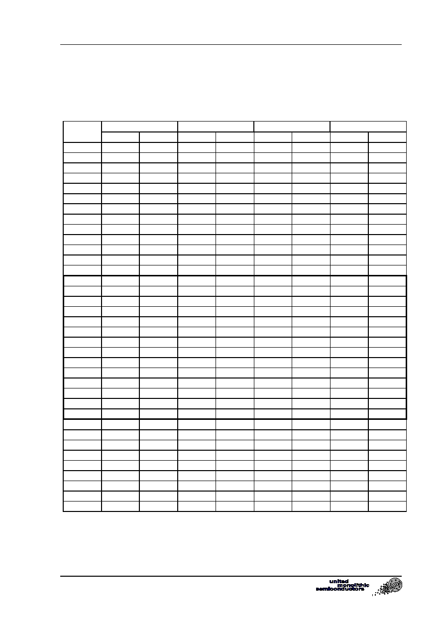
Main Characteristics
Tamb = +25∞C
Symbol
Parameter
Min
Typ
Max
Unit
NF
Noise figure,18-31GHz
2.5
3.5
dB
G
Gain
18
22
dB
G
Gain flatness
±
1
±
1.5
dB
ESD Protections : Electrostatic discharge sensitive device observe handling precautions !

CHA2069
18-31GHz Low Noise Amplifier
Ref. :DSCHA20699273 - 8-Sep-99
2
/
8
Specifications subject to change without notice
Route DÈpartementale 128 , B.P.46 - 91401 ORSAY Cedex - FRANCE
Tel.: +33 (0)1 69 33 03 08 - Fax : +33 (0)1 69 33 03 09
Electrical Characteristics
Tamb = +25∞C, Vd = +4,5V Pads:B=D=E=Gnd
Symbol
Parameter
Min
Typ
Max
Unit
Fop
Operating frequency range
18
31
Ghz
G
Gain (1)
18
22
dB
G
Gain flatness (1)
±
1
±
1.5
dB
NF
Noise figure (1)
2.5
3.5
dB
VSWRin
Input VSWR (1)
2.0:1
2.5:1
VSWRout
Ouput VSWR (1)
2:0:1
2.5:1
IP3
3rd order intercept point
20
dBm
P1dB
Output power at 1dB gain compression
10
dBm
Id
Drain bias current (2)
55
75
mA
(1) These values are representative on-wafer measurements that are made without bonding wires
at the RF ports.
(2) This current is the typical value from the low noise low consumption biasing ( B & D & E
grounded ).
Absolute Maximum Ratings
(3)
Tamb = +25∞C
Symbol
Parameter
Values
Unit
Vd
Drain bias voltage (5)
5.0
V
Pin
Maximum peak input power overdrive (4)
+15
dBm
Top
Operating temperature range
-40 to +85
∞C
Tstg
Storage temperature range
-55 to +125
∞C
(3) Operation of this device above anyone of these paramaters may cause permanent damage.
(4) Duration < 1s.
(5) See chip biasing options pp7
18-31GHz Low Noise Amplifier
CHA2069
Ref. :DSCHA20699273 - 8-Sep-99
3
/
8
Specifications subject to change without notice
Route DÈpartementale 128 , B.P.46 - 91401 ORSAY Cedex - FRANCE
Tel.: +33 (0)1 69 33 03 08 - Fax : +33 (0)1 69 33 03 09
Typical Result
Chip Typical Response ( On wafer Sij ) :
Tamb = +25∞C
VD=4.5V ID
=+55 mA
F(GHz)
S11
S12
S21
S22
mod
pha
mod
Pha
mod
pha
mod
pha
dB
deg
dB
Deg
dB
deg
dB
deg
2
-0.01
-34.9
-83.58
-127.8
-63.71
-13.4
-1.00
-119.2
4
-0.01
-71.6
-76.83
108.8
-58.71
67.0
-1.47
175.5
6
-0.15
-112.7
-66.00
60.8
-23.56
-164.4
-2.32
127.4
8
-0.74
-164.6
-71.92
-16.4
1.54
82.3
-3.60
81.3
10
-3.30
128.2
-70.19
-49.4
12.91
-27.1
-5.05
47.4
11
-5.18
90.4
-59.14
-73.7
16.99
-80.0
-5.37
16.5
12
-6.94
50.5
-54.33
-122.3
19.60
-134.0
-7.20
-11.0
13
-7.98
11.7
-51.51
-169.1
21.14
175.3
-9.15
-34.1
14
-8.31
-23.4
-50.07
149.9
21.66
129.6
-11.20
-56.3
15
-8.58
-54.0
-49.42
116.2
22.18
87.5
-13.60
-77.5
16
-9.01
-77.8
-49.02
87.9
22.07
51.3
-16.65
-96.6
17
-9.66
-97.0
-49.24
56.9
22.35
17.5
-21.01
-115.6
18
-10.27
-112.2
-49.74
38.9
22.25
-13.3
-28.25
-138.6
19
-11.44
-125.0
-48.80
9.0
22.30
-43.3
-29.93
70.6
20
-12.60
-132.7
-50.27
-20.2
22.38
-72.0
-20.66
26.9
21
-13.74
-137.8
-50.08
-36.8
22.38
-99.8
-16.29
8.9
22
-14.44
-140.0
-50.55
-62.5
22.60
-127.6
-13.67
-8.6
23
-15.21
-142.8
-51.54
-81.8
22.72
-155.4
-12.01
-23.6
24
-16.15
-144.4
-51.68
-101.2
22.60
176.7
-10.83
-36.2
25
-16.91
-142.9
-53.88
-123.9
22.65
148.6
-10.08
-48.8
26
-17.29
-139.8
-55.05
-131.7
22.52
121.6
-9.73
-59.3
27
-16.84
-139.8
-56.50
-130.9
22.33
95.0
-9.58
-69.9
28
-16.95
-147.5
-54.45
-134.4
22.31
68.4
-9.80
-78.4
29
-20.07
-167.5
-52.53
-163.2
22.38
40.0
-10.82
-83.0
30
-30.52
-155.1
-54.62
-174.1
22.26
11.1
-11.30
-83.9
31
-27.00
-17.8
-53.75
179.4
22.16
-19.5
-11.94
-81.7
32
-14.97
-22.9
-53.19
178.6
21.80
-52.8
-11.76
-73.8
33
-9.33
-43.0
-51.06
149.6
21.01
-87.4
-10.65
-68.9
34
-5.88
-63.5
-52.88
130.3
19.68
-122.9
-9.14
-68.4
35
-3.76
-82.7
-49.61
134.9
17.65
-157.6
-7.96
-71.3
36
-2.43
-100.5
-47.83
116.4
15.15
170.2
-6.97
-75.0
37
-1.79
-116.2
-52.98
85.7
12.27
141.0
-6.11
-79.3
38
-1.35
-129.6
-46.64
67.5
9.27
114.2
-5.37
-83.2
39
-1.14
-140.6
-59.58
31.3
6.10
90.1
-4.70
-87.6
40
-0.83
-151.3
-54.65
61.1
2.95
68.0
-4.13
-92.4
CHA2069
18-31GHz Low Noise Amplifier
Ref. :DSCHA20699273 - 8-Sep-99
4
/
8
Specifications subject to change without notice
Route DÈpartementale 128 , B.P.46 - 91401 ORSAY Cedex - FRANCE
Tel.: +33 (0)1 69 33 03 08 - Fax : +33 (0)1 69 33 03 09
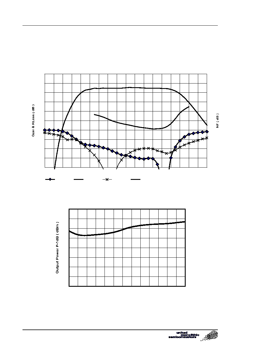
Typical Results
Chip Typical Response ( On wafer Sij ) :
Tamb = +25∞C
Vd = 4.5V ; B , D & E=GND; Id = 55mA
-20
-15
-10
-5
0
5
10
15
20
25
30
4
6
8
10
12
14
16
18
20
22
24
26
28
30
32
34
36
38
40
Frequency ( GHz )
0.0
0.5
1.0
1.5
2.0
2.5
3.0
3.5
4.0
4.5
5.0
dBS11
dBS21
dBS22
Nf
Typical Gain and Matching measurements on wafer.
0
2
4
6
8
10
12
14
16
18
20
22
24
26
28
30
Frequency ( GHz )
Typical Poutput Power -1dB measurements on wafer.

18-31GHz Low Noise Amplifier
CHA2069
Ref. :DSCHA20699273 - 8-Sep-99
5
/
8
Specifications subject to change without notice
Route DÈpartementale 128 , B.P.46 - 91401 ORSAY Cedex - FRANCE
Tel.: +33 (0)1 69 33 03 08 - Fax : +33 (0)1 69 33 03 09
Typical Test-Jig Results
Circuit Typical Response ( Test-Jig ) :
Tamb = +25∞C
Vd = 4.5V ; B ,D & E =Pads grounded ; Id = 55mA
(G1, G2, A, C & F non connected )
These values are representative of the package assembly with input and output bonding
wires of typically 0.15nH.
-20
-15
-10
-5
0
5
10
15
20
25
30
4
6
8
10
12
14
16
18
20
22
24
26
28
30
32
34
36
38
40
Frequency ( GHz )
Gain
S11
S22
T
ypical Linear measurements in test-jig.
0
0.5
1
1.5
2
2.5
3
3.5
4
4.5
5
18
20
22
24
26
28
30
32
Frequency ( GHz )
Typical NOISE Figure measurements in test-jig.