 | –≠–ª–µ–∫—Ç—Ä–æ–Ω–Ω—ã–π –∫–æ–º–ø–æ–Ω–µ–Ω—Ç: CHA2090 | –°–∫–∞—á–∞—Ç—å:  PDF PDF  ZIP ZIP |
CHA2090
Ref. : DSCHA20909347 ≠ 13 Dec. 99
1/
8
Specifications subject to change without notice
United Monolithic Semiconductors S.A.S.
Route DÈpartementale 128 - B.P.46 - 91401 Orsay Cedex France
Tel. : +33 (0)1 69 33 03 08 - Fax : +33 (0)1 69 33 03 09
17-24GHz Low Noise Amplifier
GaAs Monolithic Microwave IC
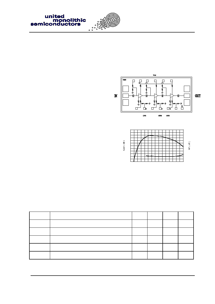
Description
The CHA2090 is a three-stage self-biased
wide band monolithic low noise amplifier.
The circuit is manufactured with a standard
HEMT process : 0.25µm gate length, via
holes through the substrate, air bridges
and electron beam gate lithography.
It is supplied in chip form.
Main Features
ß
Broadband performance 17-24GHz
ß
2.0dB noise figure
ß
23dB
gain,
±
1dB gain flatness
ß
Low DC power consumption, 55mA
ß
Chip size : 2,170 x 1,270x 0.1mm
0
5
10
15
20
25
30
5 7 9 11 13 15 17 19 21 23 25 27 29 31 33 35
Frequency ( GHz )
0
2
4
6
8
10
12
On wafer typical measurements
Main Characteristics
Tamb = +25∞C, Vd=4.5V, Pads B,D,E=GND
Symbol
Parameter
Min
Typ
Max
Unit
Fop
Operating frequency range
17
24
GHz
NF
Noise figure
2.0
3.0
dB
G
Gain
19
23
dB
VSWRin
Input VSWR
2:1
VSWRout Output VSWR
2:1
ESD Protection : Electrostatic discharge sensitive device. Observe handling precautions !

CHA2090
17-24GHz Low Noise Amplifier
Ref. : DSCHA20909347 ≠ 13 Dec. 99
2/
8
Specifications subject to change without notice
Route DÈpartementale 128 , B.P.46 - 91401 ORSAY Cedex - FRANCE
Tel.: +33 (0)1 69 33 03 08 - Fax : +33 (0)1 69 33 03 09
Main Characteristics
Tamb = +25∞C, Vd=4.5V, Pads B,D,E=GND
Symbol
Parameter
Min
Typ
Max
Unit
Fop
Operating frequency range
17
24
GHz
NF
Noise figure (1)
2
3
dB
G
Gain (1)
19
23
dB
Pout
Pout -1dB gain compression
10
dBm
VSWRin
Input VSWR (1)
2.0:1
2.5:1
VSWRout Output VSWR (1)
2.0:1
2.5:1
Vdd
Positive Drain voltage (2)
4.5
5.0
V
(1) These values are representative of on-wafer measurements that are made without bonding wires
at the RF ports. When the chip is attached with typical 0.15nH input and output bonding wires, the
indicated parameter values should be improved.
(2) See chip biasing option page 7/8.
Absolute Maximum Ratings
(1)
Tamb = +25∞C
Symbol
Parameter
Values
Unit
Vd
Drain bias voltage (3)
5.5
V
Pin
Maximum peak input power overdrive (2)
+15
dBm
Top
Operating temperature range
-40 to +85
∞C
Tstg
Storage temperature range
-55 to +125
∞C
(1) Operation of this device above anyone of these parameters may cause permanent damage.
(2) Duration < 1s.
(3) See chip biasing option page 7/8.
17-24GHz Low Noise Amplifier
CHA2090
Ref. : DSCHA20909347 ≠ 13 Dec. 99
3/
8
Specifications subject to change without notice
Route DÈpartementale 128 , B.P.46 - 91401 ORSAY Cedex - FRANCE
Tel.: +33 (0)1 69 33 03 08 - Fax : +33 (0)1 69 33 03 09
Typical Result
Chip Typical Response ( On wafer Sij ) :
Tamb = +25∞C VD = 4.5V ID = 55mA
Frequency
MS11
PS11
MS12
PS12
MS21
PS21
MS22
PS22
mod
pha
mod
pha
mod
pha
mod
pha
GHz
dB
deg
dB
deg
dB
deg
dB
deg
1.000
-0.53
-20.8
-89.62
-92.0
-41.76
-148.5
-0.72
-23.8
2.000
-0.06
-39.0
-97.43
26.6
-48.17
170.5
-0.30
-50.3
3.000
-0.10
-58.5
-87.21
-23.0
-52.46
74.5
-0.33
-75.6
4.000
-0.16
-77.4
-84.87
-135.7
-61.22
154.8
-0.49
-101.9
5.000
-0.23
-96.5
-83.35
120.1
-35.86
-69.1
-0.89
-129.8
6.000
-0.34
-115.2
-66.23
84.2
-12.12
-123.6
-1.77
-159.0
7.000
-0.35
-134.1
-72.40
-58.1
1.34
145.9
-3.35
168.8
8.000
-0.45
-154.1
-73.93
-13.6
7.48
75.4
-6.63
141.1
9.000
-0.52
-175.4
-72.23
-7.1
11.96
18.3
-9.34
119.1
10.000
-0.75
160.3
-66.01
-34.2
15.54
-28.2
-13.97
85.5
11.000
-1.21
132.1
-60.26
-60.3
18.30
-72.2
-22.57
53.2
12.000
-2.33
97.8
-56.60
-94.9
19.92
-116.5
-39.69
-60.4
13.000
-4.60
57.2
-53.53
-135.9
21.36
-163.1
-30.19
-133.1
14.000
-8.86
8.5
-52.43
-173.4
22.49
149.3
-25.30
-127.8
15.000
-16.48
-40.4
-52.50
157.8
23.60
100.6
-21.56
-134.5
16.000
-24.70
-70.2
-52.26
135.4
23.89
62.2
-19.34
-144.1
17.000
-27.75
-80.6
-52.62
108.9
24.01
28.4
-17.60
-158.0
18.000
-23.51
-87.4
-51.36
100.6
23.66
-1.9
-16.51
-172.3
19.000
-21.41
-95.7
-51.27
60.6
23.52
-30.5
-16.34
163.7
20.000
-18.63
-107.0
-54.07
52.8
23.46
-57.8
-17.75
149.6
21.000
-16.77
-115.6
-55.06
30.3
23.11
-84.4
-19.33
131.6
22.000
-14.95
-123.2
-57.35
23.7
23.14
-111.0
-22.26
113.9
23.000
-13.73
-132.0
-59.54
8.0
22.82
-137.3
-25.44
89.1
24.000
-12.59
-138.8
-60.85
32.3
22.36
-162.8
-29.95
43.8
25.000
-11.60
-144.7
-62.07
49.5
22.01
171.8
-28.26
-24.5
26.000
-10.61
-149.8
-54.29
40.2
21.46
147.9
-22.90
-58.9
27.000
-9.34
-154.5
-55.03
23.9
20.91
125.0
-19.22
-84.3
28.000
-7.89
-160.6
-52.05
-11.6
20.49
102.3
-17.12
-102.6
29.000
-6.63
-171.3
-60.41
-22.1
20.06
78.5
-16.20
-114.2
30.000
-5.86
179.9
-56.56
23.2
19.50
55.4
-14.73
-123.1
31.000
-4.83
172.0
-52.73
-13.7
19.03
31.5
-13.72
-137.5
32.000
-3.95
161.7
-54.11
-40.7
18.31
6.9
-13.60
-147.0
33.000
-3.18
151.2
-54.59
-51.2
17.51
-17.5
-13.61
-155.8
34.000
-2.61
140.2
-55.15
-37.9
16.54
-42.3
-14.22
-161.4
35.000
-2.15
129.3
-51.68
-92.2
15.35
-66.8
-14.94
-161.8
36.000
-1.77
117.9
-57.64
-111.2
13.94
-91.0
-15.31
-154.5
37.000
-1.65
106.7
-60.87
-68.5
12.41
-114.4
-13.87
-143.9
38.000
-1.64
95.9
-53.10
-33.4
10.67
-137.5
-11.60
-140.4
39.000
-1.65
85.9
-47.45
-99.7
8.76
-159.6
-9.18
-143.5
40.000
-1.76
75.2
-46.80
-137.0
6.70
178.9
-7.06
-151.0
CHA2090
17-24GHz Low Noise Amplifier
Ref. : DSCHA20909347 ≠ 13 Dec. 99
4/
8
Specifications subject to change without notice
Route DÈpartementale 128 , B.P.46 - 91401 ORSAY Cedex - FRANCE
Tel.: +33 (0)1 69 33 03 08 - Fax : +33 (0)1 69 33 03 09
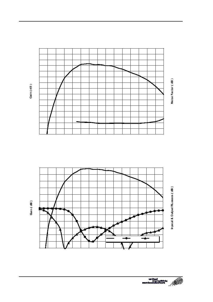
Typical on Wafer Measurements
Bias conditions: Vd = 4.5V, Id = 55mA
0
2
4
6
8
10
12
14
16
18
20
22
24
26
28
30
5
7
9
11
13
15
17
19
21
23
25
27
29
31
33
35
Frequency ( GHz )
0
1
2
3
4
5
6
7
8
9
10
11
12
13
14
15
-5
0
5
10
15
20
25
5
7
9
11
13
15
17
19
21
23
25
27
29
31
33
35
Frequency ( GHz )
-30
-25
-20
-15
-10
-5
0
5
10
15
20
25
30
Gain
dBS11
dBS22
17-24GHz Low Noise Amplifier
CHA2090
Ref. : DSCHA20909347 ≠ 13 Dec. 99
5/
8
Specifications subject to change without notice
Route DÈpartementale 128 , B.P.46 - 91401 ORSAY Cedex - FRANCE
Tel.: +33 (0)1 69 33 03 08 - Fax : +33 (0)1 69 33 03 09
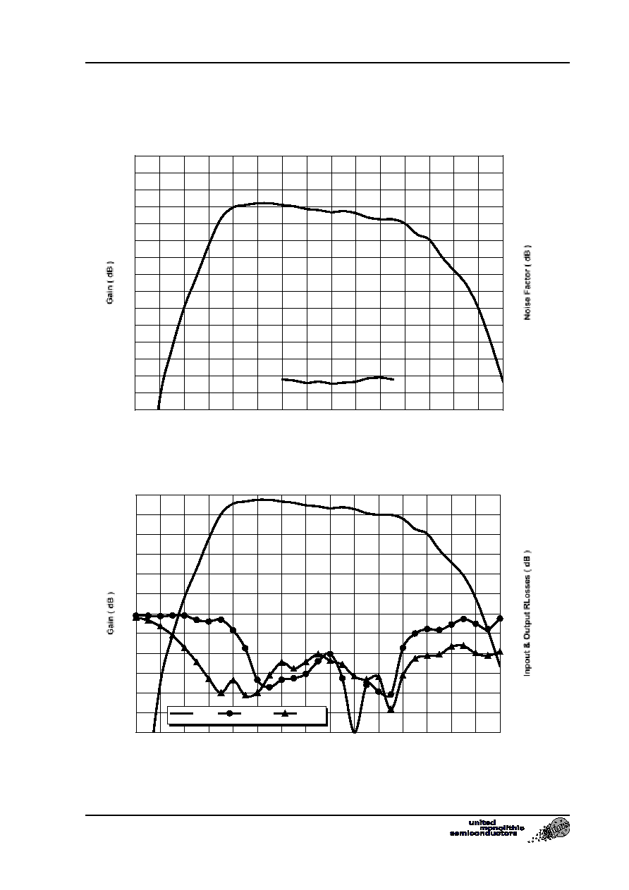
Typical on Test Jig Measurements
Bias conditions: Vd = 4.5V, Id = 55mA
0
2
4
6
8
10
12
14
16
18
20
22
24
26
28
30
5
7
9
11
13
15
17
19
21
23
25
27
29
31
33
35
Frequency ( GHz )
0
1
2
3
4
5
6
7
8
9
10
11
12
13
14
15
-5
0
5
10
15
20
25
5
7
9
11
13
15
17
19
21
23
25
27
29
31
33
35
Frequency ( GHz )
-30
-25
-20
-15
-10
-5
0
5
10
15
20
25
30
Gain
dBS11
dBS22