
CHA2093
Ref. : DSCHA20933279 - 06 Oct 03
1/8
Specifications subject to change without notice
United Monolithic Semiconductors S.A.S.
Route DÈpartementale 128 - B.P.46 - 91401 Orsay Cedex France
Tel. : +33 (0)1 69 33 03 08 - Fax : +33 (0)1 69 33 03 09
20-30GHz Low Noise Amplifier
GaAs Monolithic Microwave IC
Description
The CHA2093 is a two-stage wide band
monolithic low noise amplifier.
The circuit is manufactured with a standard
HEMT process : 0.25µm gate length, via
holes through the substrate, air bridges
and electron beam gate lithography.
It is supplied in chip form.
Main Features
Broad band performance 20-30GHz
2.2dB noise figure, 20-30GHz
15dB gain,
± 0.5dB gain flatness
Low DC power consumption, 50mA
20dBm 3rd order intercept point
Chip size : 1.67 x 1.03 x 0.1mm
IN
OUT
Vg 1
Vg 2
25
50
Vd
0
2
4
6
8
10
12
14
16
18
20
10
15
20
25
30
35
40
Frequency ( GHz )
Gain ( dB
)
0
1
2
3
4
5
6
7
8
9
10
No
ise
F
i
g
u
r
e
(
d
B
)
On wafer typical measurements.
Main Characteristics
Tamb = +25∞C
Symbol Parameter Min
Typ
Max
Unit
NF
Noise figure, 20-30GHz
2.2
3.0
dB
G Gain
13 15 dB
G
Gain flatness
± 0.5
± 1.0
dB
ESD Protections : Electrostatic discharge sensitive device observe handling precautions !
CHA2093
20-30GHz Low Noise Amplifier
Ref. : DSCHA20933279 - 06 Oct 03
2/8
Specifications subject to change without notice
Route DÈpartementale 128 , B.P.46 - 91401 ORSAY Cedex - FRANCE
Tel.: +33 (0)1 69 33 03 08 - Fax : +33 (0)1 69 33 03 09
Electrical Characteristics
Tamb = +25∞C, Vd = +4V Id=45mA
Symbol Parameter Min
Typ
Max
Unit
Fop
Operating frequency range
20
30
Ghz
G Gain
(1)
13 15 dB
G
Gain flatness (1)
± 0.5
± 1.0
dB
NF
Noise figure (1)
2.2 3.0 dB
VSWRin Input VSWR (1)
3.0:1
VSWRout Ouput VSWR (1)
3.0:1
IP3
3rd order intercept point
20
dBm
P1dB
Output power at 1dB gain compression
13 dBm
Id
Drain bias current
50
mA
(1) These values are representative of on-wafer measurements that are made without
bonding wires at the RF ports.When the chip is attached with typical 0.15nH input and
output bonding wires , the indicated parameter values should be improved.
Absolute Maximum Ratings
(1)
Tamb = +25∞C
Symbol Parameter
Values
Unit
Vd
Drain bias voltage
5.0
V
Pin
Maximum peak input power overdrive (2)
+10
dBm
Top
Operating temperature range
-40 to +85
∞C
Tstg
Storage temperature range
-55 to +125
∞C
(1) Operation of this device above anyone of these paramaters may cause permanent damage.
(2) Duration < 1s.

20-30GHz Low Noise Amplifier
CHA2093
Ref. : DSCHA20933279 - 06 Oct 03
3/8
Specifications subject to change without notice
Route DÈpartementale 128 , B.P.46 - 91401 ORSAY Cedex - FRANCE
Tel.: +33 (0)1 69 33 03 08 - Fax : +33 (0)1 69 33 03 09
Typical Results
Chip Typical Response ( On wafer Sij ) :
Tamb = +25∞C
Bias Conditions : Vd = +4V Id=45mA
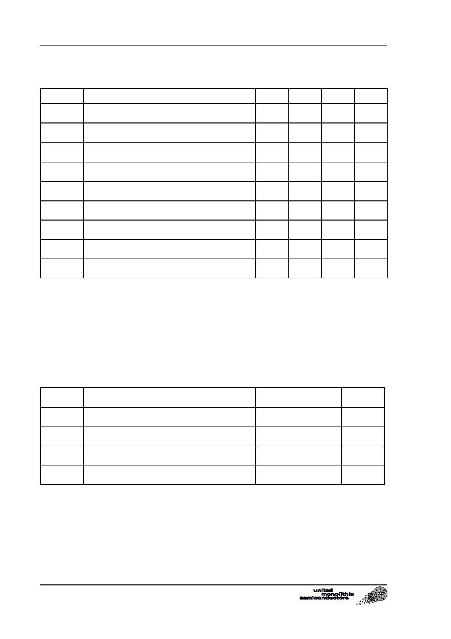
Freq
GHz
MS11
dB
PS11
∞
MS12
dB
PS12
∞
MS21
dB
PS21
∞
MS22
dB
PS22
∞
10 -1.36 140 -62.29
-138.5
4.35 51.6 -16.6
151.6
11 -1.98 121.9 -58.39 -130.1 7.36 27.2 -16.75 145.1
12 -2.93 101.1 -53.05 -130.3 9.77 0.8 -16.67 137.9
13 -4.5 77.7 -49.08 -146.8 11.61 -26.2 -16.77 129.8
14 -6.8 50.1 -46.97 -163.9 12.9 -53.2 -17.47 122.7
15 -10.02 16.4 -44.52 173.2 13.86 -78.7 -17.67 122.2
16 -13.47 -30 -42.23 160.2 14.55 -103.5
-18.06 118.4
17 -14.68 -86 -40.43 138.2 15 -127 -18.55 118.4
18 -13.76 -131 -39.41 126.2 15.36 -149.8 -18.7 125.4
19 -12.83
-159.2 -38 104.7 15.69
-171.8 -17.9 131.3
20 -13.51 177.8 -36.01 92.4 15.79 165.6 -15.62 131.1
21 -14.3
170.9
-34.99
63.7 15.96
144.3
-14.48 127
22 -14.74 167.2 -34.53 46.8 15.98 122.3 -13.4 120.5
23 -14.63 168 -34.46 24.6 15.84 102.1 -12.6 116.3
24 -14.15 163.4 -33.67 6.3 15.75 80.9 -11.67 107.1
25 -13.71 155.8 -33.27 -7.6 15.6 60.2 -11.4 100.6
26 -13.42 145.5 -32.65 -29.3 15.55 40.3 -11.3 96.1
27 -13.54 124.4 -32.6 -51.5 15.46 18.6 -10.33 91.6
28 -14.43 100.2 -32.49 -68.3 15.48 -2.8 -9.98 85.7
29 -14.48 56.9 -31.69 -88.8 15.48 -27.3 -8.88 80.2
30 -12.87 5.6 -31.87
-115.7 15.24 -53 -7.99 70.5
31 -8.84 -37.4 -31.22 -140.4 14.69 -82.2 -6.86 58.1
32 -5.55 -73.3
-31.23
-171 13.43
-112.8
-6.35 40.1
33 -3.72 -101.3 -32.96 159.7 11.43 -141.9 -6.69 20.4
34 -2.5
-123.2
-34.73
134.8
9.01
-168.7
-7.51 1.5
35 -1.88
-141.2
-35.69
121.6 6.2 167.5
-8.65 -17
36 -1.52
-155.7
-35.69 98 3.35 145.9
-9.92 -36.6
37 -1.32
-167.5
-37.95
72.2 0.36 125.7
-11.17
-56.5
38 -1.07 -177.6 -38.15 56.8 -2.78 107.4 -12.15 -78.9
39 -0.93
172.6
-43.41
86.9 -6.02 89 -12.5
-103.1
40 -0.82 164.7 -43.1 76.9 -9.59 71.9 -12.27 -127.3
41 -0.68 157.2 -43.1 44.4 -13.6 55.3 -11.82 -148.5
42 -0.52 149.5 -43.23 39.6 -18.24 40.2 -10.89 -166.3
43 -0.5 142 -44.08 24 -24.6 27.2 -9.87
-179.6
44 -0.41 135.3 -45.8 21 -35.19 30.1 -8.91 167.4
45 -0.37 128.4 -45.05 18.1 -37.14 126.8 -8.04 156.2

CHA2093
20-30GHz Low Noise Amplifier
Ref. : DSCHA20933279 - 06 Oct 03
4/8
Specifications subject to change without notice
Route DÈpartementale 128 , B.P.46 - 91401 ORSAY Cedex - FRANCE
Tel.: +33 (0)1 69 33 03 08 - Fax : +33 (0)1 69 33 03 09
Typical Results
Chip Typical Response ( On wafer Sij ) :
Tamb = +25∞C
Vd = 4V ; Id = 45mA
-20
-15
-10
-5
0
5
10
15
20
10
12
14
16
18
20
22
24
26
28
30
32
34
36
38
40
Frequency ( GHz )
G
a
in, RLoss ( dB )
DBS11
DBS22
Gain
Typical Gain and Matching measurements on wafer.
0
1
2
3
4
5
6
7
8
9
10
11
12
13
14
15
16
17
18
19
20
15 16 17 18 19 20 21 22 23 24 25 26 27 28 29 30 31 32 33 34
Frequency ( GHz )
Ga
in, N
F
( dB
)
Gain
NF
Gab
Typical Gain and Noise Figure measurements on wafer.

20-30GHz Low Noise Amplifier
CHA2093
Ref. : DSCHA20933279 - 06 Oct 03
5/8
Specifications subject to change without notice
Route DÈpartementale 128 , B.P.46 - 91401 ORSAY Cedex - FRANCE
Tel.: +33 (0)1 69 33 03 08 - Fax : +33 (0)1 69 33 03 09
Typical Results
Tamb = +25∞C
Vd = 4V ; Id = 45mA
0
2
4
6
8
10
12
14
16
-9 -8 -7 -6 -5 -4 -3 -2 -1
0
1
2
3
4
5
Input power (dBm)
O
u
tput power
(
d
Bm
)
0
2
4
6
8
10
12
14
16
F=20GHz
Ga
s
s
(d
B)
Pout
Gain
0
2
4
6
8
10
12
14
16
-3
-2
-1
0
1
2
3
4
5
6
7
Input power (dBm)
O
u
tput power
(
d
Bm
)
0
2
4
6
8
10
12
14
16
F=30GHz
Ga
s
s
(d
B)
Pout
Gain
Typical Output Power and Gain measurements in test jig
(included losses of the jig)

CHA2093
20-30GHz Low Noise Amplifier
Ref. : DSCHA20933279 - 06 Oct 03
6/8
Specifications subject to change without notice
Route DÈpartementale 128 , B.P.46 - 91401 ORSAY Cedex - FRANCE
Tel.: +33 (0)1 69 33 03 08 - Fax : +33 (0)1 69 33 03 09
Typical Chip Assembly
25
50
To Vd DC Drain supply feed
To Vg1 DC Gate supply feed
To Vg2 DC Gate supply feed
100pF
100pF
100pF
IN
OUT
7034
Mechanical data

20-30GHz Low Noise Amplifier
CHA2093
Ref. : DSCHA20933279 - 06 Oct 03
7/8
Specifications subject to change without notice
Route DÈpartementale 128 , B.P.46 - 91401 ORSAY Cedex - FRANCE
Tel.: +33 (0)1 69 33 03 08 - Fax : +33 (0)1 69 33 03 09
Chip Biasing
This chip is a two stage amplifier, and flexibility is provided by the access to number of pads.
The internal DC electrical schematic is given in order to use these pads in a safe way.
IN
OUT
Vg 1
Vg 2
25
50
Vd
Vds1
Vds2
The two requirements are :
N∞1 : Not exceed Vds = 3.5V
( internal Drain to Source voltage ).
N∞2 : Not biased in such a way that Vgs becomes positive.
( internal Gate to Source voltage )
We propose two standard biasing :
Low Noise and low consumption :
Vd = 3.5V and Id = 30mA ( Vg1=Vg2)
Low Noise and high output power :
Vd = 4.0V and Id = 45mA. A separate access to
the gate voltages of the first and the output stage is provided. Nominal bias is obtained for a
typical current of 30mA for the output stage and 15 mA for the first stage. The first step to
bias the amplifier is to tune the Vg1 =-1V and Vg2 to drive 30mA for the full amplifier. Then
Vg1 is reduced to obtain 45 mA of current through the amplifier.

CHA2093
20-30GHz Low Noise Amplifier
Ref. : DSCHA20933279 - 06 Oct 03
8/8
Specifications subject to change without notice
Route DÈpartementale 128 , B.P.46 - 91401 ORSAY Cedex - FRANCE
Tel.: +33 (0)1 69 33 03 08 - Fax : +33 (0)1 69 33 03 09
Ordering Information
Chip form :
CHA2093-99F/00
Information furnished is believed to be accurate and reliable. However United Monolithic Semiconductors
S.A.S. assumes no responsability for the consequences of use of such information nor for any infringement of
patents or other rights of third parties which may result from its use. No license is granted by implication or
otherwise under any patent or patent rights of United Monolithic Semiconductors S.A.S.. Specifications
mentioned in this publication are subject to change without notice. This publication supersedes and replaces all
information previously supplied. United Monolithic Semiconductors S.A.S. products are not authorised for use
as critical components in life support devices or systems without express written approval from United
Monolithic Semiconductors S.A.S.