
CHA2093RBF
Ref. : DSCHA2093RBF2057 -26-Feb.-02-
1/8
Specifications subject to change without notice
United Monolithic Semiconductors S.A.S.
Route DÈpartementale 128 - B.P.46 - 91401 Orsay Cedex France
Tel. : +33 (0)1 69 33 03 08 - Fax : +33 (0)1 69 33 03 09
20-30GHz Low Noise Amplifier
GaAs Monolithic Microwave IC in SMD leadless package
Description
The monolithic microwave IC (MMIC) in the
package is a two-stage wide band
monolithic low noise amplifier.
The circuit is manufactured with a standard
PHEMT process : 0.25µm gate length, via
holes through the substrate, air bridges
and electron beam gate lithography.
It is supplied in a new SMD leadless chip
carrier.
Main Features
Broad band performance: 20-30GHz
Gain = 14dB (typical)
Noise Figure 3.0dB (typical)
Return loss < -7dB
Low DC consumption < 50mA
SMD leadless package
Dimensions: 5.08 x 5.08 x 0.97 mm
3
SMD Package Dimensions
"Please note that PIN 1 is located in the lower left corner of the package (front-side view) for all SMD-type packages from United Monolithic Semiconductors. It is indicated
by a triangle on the package lid. Starting with PIN 1 the other pads are numbered counter-clockwise (front-side view). ATTENTION: The dot on the backside of the
package (i.e. side with metallic pads) is just for fabrication purposes and does NOT indicate the location of PIN 1."

CHA2093RBF
20-30GHz Low Noise Amplifier
Ref. : DSCHA2093RBF2057 -26-Feb.-02-
2/8
Specifications subject to change without notice
Route DÈpartementale 128 , B.P.46 - 91401 ORSAY Cedex - FRANCE
Tel.: +33 (0)1 69 33 03 08 - Fax : +33 (0)1 69 33 03 09
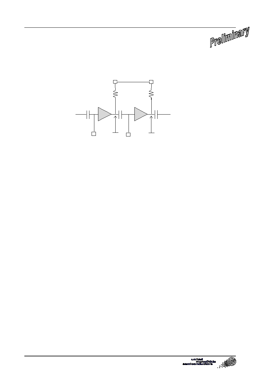
Schematic
Typical Bias Conditions
for an ambient Temperature of +25∞C
Symbol Pin
No.
Parameter
Values Unit
Vdd
5
Drain bias voltage
4
V
Vg1 & 2
1 & 2
First & second stages gate bias voltage
-0.2
V
Id 5
Drain
current
45
mA
All other pins are not used for this device.
Absolute Maximum Ratings
(1)
Tamb = +25∞C
Symbol Parameter
Values
Unit
Vd
Drain bias voltage
4.0
V
Pin
Maximum peak input power overdrive (2)
+15
dBm
Top
Operating temperature range (3)
-40 to +85
∞C
Tstg
Storage temperature range
-55 to +125
∞C
(1) Operation of this device above anyone of these paramaters may cause permanent damage.
(2) Duration < 1s.
(3) Upper temperature limit strongly dependent on motherboard design; ratings given for
ideal thermal coupling

20-30GHz Low Noise Amplifier
CHA2093RBF
Ref. : DSCHA2093RBF2057 -26-Feb.-02-
3/8
Specifications subject to change without notice
Route DÈpartementale 128 , B.P.46 - 91401 ORSAY Cedex - FRANCE
Tel.: +33 (0)1 69 33 03 08 - Fax : +33 (0)1 69 33 03 09
Typical results on PCB (recommended motherboard layout)
Vd=4V, Id adjusted at 45mA
Gain & Return Loss
-20
-18
-16
-14
-12
-10
-8
-6
-4
-2
0
2
4
6
8
10
12
14
16
18
20
18
20
22
24
26
28
30
32
Frequency (GHz)
Linear Gain (dB)
Input Return Loss (dB)
Output Return Loss (dB)
Noise Figure (dB)
0
1
2
3
4
5
6
20
21
22
23
24
25
26
27
28
29
30
Frequency (GHz)
CHA2093RBF
20-30GHz Low Noise Amplifier
Ref. : DSCHA2093RBF2057 -26-Feb.-02-
4/8
Specifications subject to change without notice
Route DÈpartementale 128 , B.P.46 - 91401 ORSAY Cedex - FRANCE
Tel.: +33 (0)1 69 33 03 08 - Fax : +33 (0)1 69 33 03 09
Biasing Options
This chip inside the SMD type package is a two stage amplifier, and flexibility is provided by
the access to number of pads. The internal DC electrical schematic is given in order to use
these pads in a safe way.
IN
OUT
Vg 1
Vg 2
25
50
Vd
Vds1
Vds2
The two requirements are :
N∞1: Not exceed Vds = 3.5Volt ( internal Drain to Source voltage ).
N∞2: Not biased in such a way that Vgs becomes positive.
( internal Gate to Source voltage )
We propose two standard biasing :
1)
Low Noise and low consumption :
Vd = 3.5V and Id = 30mA ( Vg1=Vg2)
2)
Low Noise and high output power :
Vd = 4.0V and Id = 45mA.
(A separate acces to the gate voltages of the first and the output stage is provided.
Nominal bias is obtained for a typical current of 30mA for the output stage and 15 mA
for the first stage. The first step to bias the amplifier is to tune the Vg1 =-1V and Vg2
to drive 30mA for the full amplifier. Then Vg1 is reduced to obtain 45 mA of current
through the amplifier.)

20-30GHz Low Noise Amplifier
CHA2093RBF
Ref. : DSCHA2093RBF2057 -26-Feb.-02-
5/8
Specifications subject to change without notice
Route DÈpartementale 128 , B.P.46 - 91401 ORSAY Cedex - FRANCE
Tel.: +33 (0)1 69 33 03 08 - Fax : +33 (0)1 69 33 03 09
Footprint