
CHA2094b
Ref. : DSCHA20949312 ≠ 08-Nov.-99
1/8
Specifications subject to change without notice
United Monolithic Semiconductors S.A.S.
Route Dťpartementale 128 - B.P.46 - 91401 Orsay Cedex France
Tel. : +33 (0)1 69 33 03 08 - Fax : +33 (0)1 69 33 03 09
36-40GHz Low Noise High Gain Amplifier
GaAs Monolithic Microwave IC
Description
The CHA2094 is a three-stage monolithic low
noise amplifier. It is designed for a wide range
of applications, from military to commercial
communication systems.
The circuit is manufactured with a HEMT
process : 0.25Ķm gate length, via holes through
the substrate, air bridges and electron beam
gate lithography.
It is available in chip form.
Main Features
Broadband performances : 36-40GHz
3.0dB Noise Figure
21dB gain
Ī
1.5dB gain flatness
Low DC power consumption, 60mA @ 3.5V
Chip size :
1.72 X 1.08 X 0.10 mm
Vgs1&2
Vgs3
Vds
IN
OUT
Vds
Typical on wafer measurements :
Frequency (GHz)
Gain & NF ( dB )
0
4
8
12
16
20
24
34
35
36
37
38
39
40
41
42
Main Characteristics
Tamb. = 25įC
Symbol
Parameter
Min
Typ
Max
Unit
Fop
Operating frequency range
36
40
GHz
G
Small signal gain
18
21
dB
P1dB
Output power at 1dB gain compression
5
8
dBm
NF
Noise figure
3.0
4.0
dB
ESD Protection : Electrostatic discharge sensitive device. Observe handling precautions !

CHA2094b
36-40GHz Low Noise Amplifier
Ref. : DSCHA20949312 ≠ 08-Nov.-99
2/8
Specifications subject to change without notice
Route Dťpartementale 128 , B.P.46 - 91401 ORSAY Cedex - FRANCE
Tel.: +33 (0)1 69 33 03 08 - Fax : +33 (0)1 69 33 03 09
Electrical Characteristics
Tamb = +25įC, Vd1,2,3 = 3.5V
Symbol
Parameter
Min
Typ
Max
Unit
Fop
Operating frequency range (1)
36
40
GHz
G
Small signal gain (1)
18
21
dB
G
Small signal gain flatness (1)
Ī
1.5
dB
Gsb
Gain flatness over 40MHz ( within -30 ; +75įC )
0.5
dBpp
Is
Reverse isolation (1)
25
30
dB
P1dB
Output power at 1dB gain compression
5
8
dBm
VSWRin
Input VSWR (1)
2.5:1
3.0:1
VSWRout
Output VSWR (1)
2.5:1
3.0:1
NF
Noise figure (2)
3.0
4.0
dB
Vd
DC Voltage
Vd
Vg
-2
3.5
-0.25
4
+0.4
V
V
Id
Bias current (2)
60
100
mA
(1) These values are representative of on-wafer measurements that are made without bonding
wires at the RF ports.
(2) 60 mA is the typical bias current used for on wafer measurements, with Vg1,2 = Vg3. For
optimum noise figure, the bias current could be reduced down to 40 mA, adjusting the Vg1,2
voltage.
Absolute Maximum Ratings
Tamb. = 25įC (1)
Symbol
Parameter
Values
Unit
Vd
Drain bias voltage
5.0
V
Id
Drain bias current
150
mA
Vg
Gate bias voltage
-2.0 to +0.4
V
Pin
Maximum peak input power overdrive (2)
+15
dBm
Ta
Operating temperature range
-40 to +85
įC
Tstg
Storage temperature range
-55 to +155
įC
(1) Operation of this device above anyone of these parameters may cause permanent damage.
(2) Duration < 1s.

36-40GHz Low Noise Amplifier
CHA2094b
Ref. : DSCHA20949312 ≠ 08-Nov.-99
3/8
Specifications subject to change without notice
Route Dťpartementale 128 , B.P.46 - 91401 ORSAY Cedex - FRANCE
Tel.: +33 (0)1 69 33 03 08 - Fax : +33 (0)1 69 33 03 09
Typical Scattering Parameters ( On wafer Sij measurements )
Bias Conditions :
Vd = 3.5 Volt, Id = 60 mA.
Freq.
GHz
S11
dB
S11
/
/
į
S12
dB
S12
/
/
į
S21
dB
S21
/
/
į
S22
dB
S22
/
/
į
25,00
-2,96
165,27
-48,02
140,03
-16,95
-110,44
-10,05
-118,86
26,00
-3,22
155,96
-49,76
133,48
-11,32
-109,43
-10,84
-124,50
27,00
-3,67
144,32
-51,68
113,25
-5,73
-112,96
-11,84
-133,29
28,00
-4,43
129,06
-53,38
148,20
0,02
-123,12
-13,68
-140,35
29,00
-5,76
107,80
-51,07
153,30
5,87
-138,63
-15,98
-152,02
30,00
-8,60
75,37
-49,11
129,75
11,83
-163,77
-21,67
-162,85
31,00
-15,20
16,43
-43,10
102,32
17,22
158,34
-29,55
-46,20
32,00
-24,70
-117,32
-41,34
47,85
19,91
110,72
-17,96
-70,62
33,00
-32,32
128,04
-41,14
-5,29
20,48
71,50
-17,40
-106,13
34,00
-21,29
-38,29
-40,51
-43,14
20,60
40,20
-19,96
-133,62
35,00
-14,52
-70,72
-39,47
-69,20
20,79
12,71
-24,56
178,55
36,00
-11,33
-94,87
-38,30
-90,11
20,92
-13,60
-24,34
95,27
37,00
-9,96
-113,38
-37,80
-109,61
20,87
-38,94
-18,55
56,67
38,00
-9,89
-129,95
-35,94
-126,74
20,54
-63,47
-14,97
35,23
39,00
-10,20
-144,39
-35,21
-146,49
19,98
-85,35
-13,19
15,89
40,00
-11,51
-153,53
-34,78
-160,72
19,57
-105,56
-11,91
7,58
41,00
-13,21
-157,59
-34,26
-175,92
18,86
-125,69
-10,90
-5,61
42,00
-13,92
-154,55
-33,87
172,60
18,41
-143,91
-10,93
-16,38
43,00
-13,55
-158,17
-33,94
156,97
18,09
-160,70
-11,24
-20,60
44,00
-13,26
-169,25
-33,11
149,30
17,84
-178,94
-10,76
-22,75
45,00
-12,63
174,58
-32,50
134,15
17,56
162,79
-10,73
-25,23
46,00
-11,41
151,40
-32,48
126,00
17,17
143,77
-10,27
-26,04
47,00
-10,18
125,52
-31,57
119,05
16,79
124,08
-9,19
-30,65
48,00
-8,38
94,26
-29,97
102,75
16,21
102,47
-8,20
-37,96
49,00
-5,83
71,80
-31,11
79,31
15,23
80,21
-7,79
-48,28
50,00
-4,17
49,01
-32,37
66,58
13,86
58,54
-7,34
-61,88
51,00
-2,17
29,23
-36,86
59,57
12,36
38,69
-8,29
-75,36
52,00
-1,17
11,23
-34,48
52,60
10,48
19,05
-9,08
-85,34
53,00
-0,84
-2,48
-38,67
15,86
8,26
1,67
-9,77
-96,49
54,00
-0,55
-14,01
-40,49
-6,97
5,94
-13,96
-10,59
-106,13
55,00
-0,36
-22,96
-42,95
-5,11
3,49
-27,62
-11,16
-116,76
CHA2094b
36-40GHz Low Noise Amplifier
Ref. : DSCHA20949312 ≠ 08-Nov.-99
4/8
Specifications subject to change without notice
Route Dťpartementale 128 , B.P.46 - 91401 ORSAY Cedex - FRANCE
Tel.: +33 (0)1 69 33 03 08 - Fax : +33 (0)1 69 33 03 09
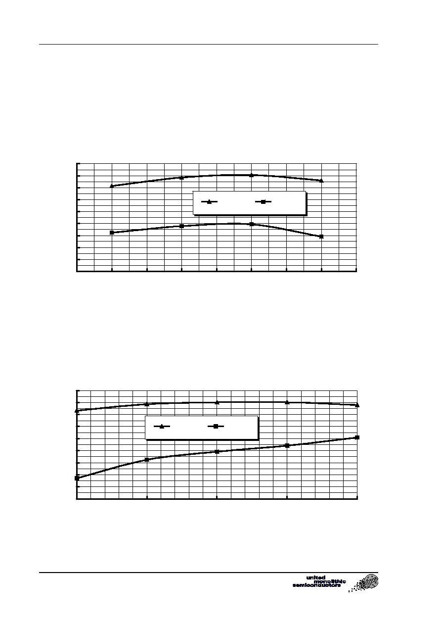
Typical Output Power ( P-1dB gain compression ) Measurements.
( CW on wafer )
Conditions : Vd = 3.5 Volt, Frequency = 38 GHz.
4
6
8
10
12
14
16
18
20
22
20
30
40
50
60
70
80
90
100
Current Id ( mA )
Gain & P-1dB ( dB, dBm )
Gain
P-1dB
Conditions : Id = 60 mA, Frequency = 38 GHz.
4
6
8
10
12
14
16
18
20
22
2.5
3
3.5
4
4.5
Bias voltage Vd ( Volt )
Gain & P-1dB ( dB, dBm )
Gain
P-1dB

36-40GHz Low Noise Amplifier
CHA2094b
Ref. : DSCHA20949312 ≠ 08-Nov.-99
5/8
Specifications subject to change without notice
Route Dťpartementale 128 , B.P.46 - 91401 ORSAY Cedex - FRANCE
Tel.: +33 (0)1 69 33 03 08 - Fax : +33 (0)1 69 33 03 09
Typical ( Gain & NF ) versus Id Measurements ( on wafer ).
Conditions : Vd = 3.5 Volt, Frequency = 38 GHz.
4
9
14
19
24
0
10
20
30
40
50
60
70
80
90
100
Current Id ( mA )
Gain ( dB )
0
1
2
3
4
5
6
7
8
9
10
NF ( dB )
Gain
NF
Typical Measurements in Test Jig.
Bias Conditions :
Vd = 3.5 Volt, Id = 50 mA.
4
9
14
19
24
36
37
38
39
40
41
42
43
44
45
46
47
Frequency ( GHz )
Gain ( dB )
0
1
2
3
4
5
6
7
8
9
10
NF ( dB )
GAIN
NF

CHA2094b
36-40GHz Low Noise Amplifier
Ref. : DSCHA20949312 ≠ 08-Nov.-99
6/8
Specifications subject to change without notice
Route Dťpartementale 128 , B.P.46 - 91401 ORSAY Cedex - FRANCE
Tel.: +33 (0)1 69 33 03 08 - Fax : +33 (0)1 69 33 03 09
Typical Bias Tuning for Low Noise Operation
The circuit schematic is given below :
IN
OUT
Vd
Vg 1,2
Vg 3
100
100
50
For low noise operation, a separate access to the gate voltages of the two first stages ( Vgs1&2 ), and
of the output stage ( Vgs3 ) is provided.
Nominal bias for low noise operation is obtained for a typical current of 20 mA for the output stage
and 15 mA for each of the two first stages ( 50 mA for the amplifier ).
The first step to bias the amplifier is to tune the Vgs1&2 = -1V, and Vgs3 to drive 20 mA for the full
amplifier. Then Vgs1&2 is reduced to obtain 50 mA of current through the amplifier.
A fine tuning of the noise figure may be obtained by modifying the Vgs1&2 bias voltage, but keeping
the previous value for Vgs3.

36-40GHz Low Noise Amplifier
CHA2094b
Ref. : DSCHA20949312 ≠ 08-Nov.-99
7/8
Specifications subject to change without notice
Route Dťpartementale 128 , B.P.46 - 91401 ORSAY Cedex - FRANCE
Tel.: +33 (0)1 69 33 03 08 - Fax : +33 (0)1 69 33 03 09
Chip Assembly and Mechanical Data
To Vdd DC Drain supply feed
To Vgs 1&2 DC Gate supply feed
To Vgs 3 DC Gate supply feed
100pF
100pF
100pF
IN
OUT
Note : Supply feed should be capacitively bypassed.
1720
Ī
10
1125
505
1080
Ī
10
415
340
415
710
Bonding pad positions.
( Chip thickness : 100Ķm. All dimensions are in micrometers )

CHA2094b
36-40GHz Low Noise Amplifier
Ref. : DSCHA20949312 ≠ 08-Nov.-99
8/8
Specifications subject to change without notice
Route Dťpartementale 128 , B.P.46 - 91401 ORSAY Cedex - FRANCE
Tel.: +33 (0)1 69 33 03 08 - Fax : +33 (0)1 69 33 03 09
Ordering Information
Chip form
:
CHA2094b99F/00
Information furnished is believed to be accurate and reliable. However United Monolithic Semiconductors
S.A.S. assumes no responsibility for the consequences of use of such information nor for any infringement of
patents or other rights of third parties which may result from its use. No license is granted by implication or
otherwise under any patent or patent rights of United Monolithic Semiconductors S.A.S.. Specifications
mentioned in this publication are subject to change without notice. This publication supersedes and replaces all
information previously supplied. United Monolithic Semiconductors S.A.S. products are not authorised for
use as critical components in life support devices or systems without express written approval from United
Monolithic Semiconductors S.A.S.