
CHA2097a
Ref. : DSCHA20978021
1/8
Specifications subject to change without notice
United Monolithic Semiconductors S.A.S.
Route DÈpartementale 128 - B.P.46 - 91401 Orsay Cedex France
Tel. : +33 (0)1 69 33 03 08 - Fax : +33 (0)1 69 33 03 09
20-40GHz Variable Gain Amplifier
GaAs Monolithic Microwave IC
Description
The CHA2097a is a variable gain broadband
three-stage monolithic amplifier. It is designed
for a wide range of applications, from military to
commercial communication systems.
The
backside of the chip is both RF and DC grounds.
This helps simplify the assembly process.
The circuit is manufactured with a PM-HEMT
process, 0.25µm gate length, via holes through
the substrate, air bridges and electron beam
gate lithography.
It is available in chip form.
Main Features
Broadband performances : 20-40GHz
14dBm output power ( 1dB gain comp. )
18dB
±
1.5dB gain
10dB gain control range.
Low DC power consumption, 140mA @ 3.5V
Chip size : 2.04 X 0.97 X 0.10 mm
Vd1 Vd23
Vctrl Vg1 Vg2 Vg3
In
Out
Main Characteristics
Tamb. = 25∞C
Symbol
Parameter
Min
Typ
Max
Unit
Fop
Operating frequency range
20
40
GHz
G
Small signal gain
16
18
dB
Gctrl
Gain control range
10
dB
P1dB
Output power at 1dB gain compression
13
14
dBm
Id
Bias current
140
200
mA
ESD Protection : Electrostatic discharge sensitive device. Observe handling precautions !
Typical on wafer measurements
-25
-20
-15
-10
-5
0
5
10
15
20
25
0
10
20
30
40
50
60
frequency (GHz)
G
a
in &
Rlos
s
(dB
)
S22
S11
CHA2097a
20-40GHz Variable Gain Amplifier
Ref. : DSCHA20978021
2/
8
Specifications subject to change without notice
Route DÈpartementale 128 , B.P.46 - 91401 ORSAY Cedex - FRANCE
Tel.: +33 (0)1 69 33 03 08 - Fax : +33 (0)1 69 33 03 09
Electrical Characteristics for Broadband Operation
Tamb = +25∞C, Vd1,2,3 = 3.5V
Symbol
Parameter
Min
Typ
Max
Unit
Fop
Operating frequency range (1)
20
40
GHz
G
Small signal gain (1)
16
18
dB
G
Small signal gain flatness (1)
±
1.5
dB
Is
Reverse isolation (1)
40
dB
P1dB
Output power at 1dB gain compression (1)
13
14
dBm
P03
Output power at 3dB gain compression
15
16
dBm
VSWRin
Input VSWR (1)
3.0:1
VSWRout Output VSWR (1)
3.0:1
Gctrl
Gain control dynamic
12
dB
Vdc
DC voltage
Vd
Vg
Vctrl
-2.0
-2.0
3.5
4.0
0.4
0.4
V
V
V
Id
Bias current
140
200
mA
(1) These values are representative of on-wafer measurements that are made without bonding
wires at the RF ports.
Absolute Maximum Ratings
Tamb. = 25∞C (1)
Symbol
Parameter
Values
Unit
Vd
Drain bias voltage
4.0
V
Id
Drain bias current
200
mA
Vg
Gate bias voltage
-2.0 to +0.4
V
Ta
Operating temperature range
-40 to +85
∞C
Tstg
Storage temperature range
-55 to +155
∞C
(1) Operation of this device above anyone of these parameters may cause permanent damage.

20-40GHz Variable Gain Amplifier
CHA2097a
Ref. : DSCHA20978021
3/8
Specifications subject to change without notice
Route DÈpartementale 128 , B.P.46 - 91401 ORSAY Cedex - FRANCE
Tel.: +33 (0)1 69 33 03 08 - Fax : +33 (0)1 69 33 03 09
Typical Scattering Parameters (On wafer Sij measurements):
Bias Conditions:
Vd=3.5V, Vg=0V, Vctrl=-1V, Id=140mA
F(GHz)
S11
S11
S12
S12
S21
S21
S22
S22
dB
/∞
dB
/∞
dB
/∞
dB
/∞
10
-4,75
-115,2
-67,47
-177,7
3,66
-94,8
-3,4
-177,9
11
-5,92
-124
-67,62
150,7
6,93
-125,4
-3,95
167,5
12
-6,95
-131
-66,42
148,4
9,91
-157,6
-4,6
152,2
13
-8,07
-137,6
-70,21
118,4
12,47
170,1
-5,43
135,1
14
-9
-142,7
-71,68
102,8
14,8
136,8
-6,68
115,1
15
-9,96
-147,7
-69,5
-77,6
16,79
101,8
-8,99
90,3
16
-10,75
-151,4
-71,34
-153,6
18,03
66,8
-12,02
64,8
17
-11,26
-154,7
-61,82
-169,2
18,79
31,6
-17,57
28,2
18
-11,52
-160,8
-58,85
171,5
19
0,7
-23,88
-12
19
-12,03
-170,5
-55,51
126,7
19,51
-29,1
-20,12
-71,4
20
-12,71
-179,1
-54,34
111,5
19,91
-57,6
-16,3
-97,4
21
-14,68
174,8
-50,54
51,9
19,56
-93,1
-10,26
-139,8
22
-14,55
168,3
-68,27
-0,3
19,32
-113,6
-11,59
-176,9
23
-17,06
154,2
-55,58
74,8
19,23
-134
-15,39
170,8
24
-19,6
155,1
-55,02
34,8
19,68
-161,4
-15,8
-174,6
25
-21,82
160,7
-54,34
25,3
19,69
172,4
-14,44
-170,8
26
-21,99
166
-52,57
4,1
19,71
147,7
-12,93
-176,7
27
-23,66
162,2
-53,35
-36,2
19,75
121,7
-12,25
174,8
28
-24,37
169
-55,75
-48,6
19,57
96
-11,11
169,8
29
-24,22
171,5
-53,54
-47,9
19,23
71,9
-10,96
156,3
30
-25,56
178,6
-56,09
-85,8
19,19
48,2
-10,95
149,1
31
-24,43
177,5
-52,89
-80,7
19,09
24,1
-11,22
142
32
-25,44
169,7
-51,25
-117,3
19,02
-0,4
-11,25
137
33
-25,52
171,3
-49,33
-147,8
18,95
-25,9
-10,52
130
34
-26,11
165,7
-50,85
-165,7
18,79
-50,8
-10,42
120,3
35
-26,98
157,4
-47,32
174,7
18,71
-76,2
-10,4
112,1
36
-28,03
132,1
-47,19
145,5
18,71
-102,2
-10,59
102,2
37
-29,59
80
-45,61
115
18,5
-130,4
-10,34
93
38
-25,97
10,7
-45,29
68,8
18,31
-158
-10,39
81,8
39
-19,91
-36,7
-48,48
57,1
18,2
172,1
-10,1
75,9
40
-15,11
-70
-47,05
65,8
17,69
139,1
-9,2
62,2
41
-11,72
-101
-45,42
28,8
16,63
105,7
-8,86
48,1
42
-9,51
-133,1
-46,37
-3,4
15,5
71,9
-8,56
35,7
43
-8,19
-167,2
-49,95
-13,7
13,76
37,9
-8,16
19,1
44
-7,23
160,6
-49,34
-29,7
11,68
4,6
-7,96
2,8
45
-6,98
127,9
-48,29
-64,6
9,12
-26,4
-7,6
-10,6
46
-7
95,8
-43,43
-46,4
6,31
-56
-7,27
-24,1
47
-6,99
64,6
-41,24
-68,1
3,32
-83,9
-7,08
-38,4
48
-6,78
34,2
-38,37
-97,4
0,15
-111,7
-6,78
-50,8
49
-6,66
7,2
-40,96
-138,5
-3,25
-137,9
-6,27
-62,1
50
-6,47
-18,1
-46,95
-70,4
-6,78
-160,6
-5,98
-75,1
51
-6,32
-40,8
-42,32
-101,2
-11,11
-178,6
-5,72
-83,4
52
-6,05
-60,5
-40,63
-176,6
-14,83
163,5
-5,3
-93,5
53
-5,89
-77,5
-48,84
171,4
-19,24
157,2
-5,1
-102,7
54
-5,71
-94,2
-61,19
111,7
-21,88
148,7
-4,8
-110,9
55
-5,58
-107,5
-56,96
103,7
-24,47
133,5
-4,35
-120,8
56
-5,1
-121,6
-55,14
166,4
-24,78
114,8
-4,18
-130,4
57
-5,23
-132,4
-50,04
30,3
-25,65
89,9
-3,86
-135,8
58
-4,98
-144,5
-54,03
-125,9
-28,47
60,3
-3,47
-145,5
59
-5,18
-155,1
-55,65
179,7
-30,93
30,8
-3,21
-153,3
CHA2097a
20-40GHz Variable Gain Amplifier
Ref. : DSCHA20978021
4/
8
Specifications subject to change without notice
Route DÈpartementale 128 , B.P.46 - 91401 ORSAY Cedex - FRANCE
Tel.: +33 (0)1 69 33 03 08 - Fax : +33 (0)1 69 33 03 09
Typical Scattering Parameters (On wafer Sij measurements):
Bias Conditions:
Vd=3.5V, Vg=0V, Vctrl=-0.3V, Id=140mA
F(GHz)
S11
S11
S12
S12
S21
S21
S22
S22
dB
/∞
dB
/∞
dB
/∞
dB
/∞
10
-21,22
-127,3
-76,73
178,5
-11,95
-77,4
-3,39
-178
11
-21,29
-137,1
-78,25
152,7
-8,66
-105,2
-3,93
167,4
12
-21,49
-145,7
-73,34
145,3
-5,6
-134,7
-4,58
152
13
-21,84
-154
-77,33
154,5
-3
-164,1
-5,41
134,8
14
-22,04
-162,3
-80,66
144,3
-0,57
165,1
-6,66
114,6
15
-22,52
-169,6
-81,88
-119,4
1,48
132,5
-8,92
89,7
16
-23,04
-176,4
-73,48
178,9
2,82
99,7
-11,91
63,8
17
-23,85
176,4
-63,82
-174,9
3,65
66,3
-17,29
26,6
18
-24,42
170,9
-64
179,2
3,85
36,8
-23,56
-16,2
19
-24,63
166
-58,81
153
4,28
8,4
-20,1
-74,1
20
-25,23
161,6
-58,94
135,1
4,54
-17,9
-16,45
-99,5
21
-26,25
153,4
-56,1
60,4
4,29
-50,3
-10,67
-138,7
22
-27,04
152,8
-76,98
-105,4
3,55
-70,1
-11,7
-175,2
23
-27,88
146,8
-61,65
138,4
3,75
-88,5
-15,43
170
24
-29,52
142,3
-59,54
99,5
4,18
-112,8
-16,32
-173,1
25
-31,05
139
-57,85
87,5
4,17
-136,4
-14,56
-168,2
26
-33,21
137,1
-58,27
78
4,12
-158,7
-13,03
-174,9
27
-36,65
139,9
-58,68
57,7
4,14
177,6
-12,27
177
28
-37,81
150,3
-59,11
58,8
3,85
154,7
-11,04
171,7
29
-38,63
-179,8
-57,44
39
3,45
133,2
-10,84
157,6
30
-36,35
-146,1
-70,19
57,9
3,32
111,7
-10,88
149,5
31
-34,9
-140,8
-56
15,6
3,14
91,1
-11,32
142,3
32
-33,79
-133,8
-64,97
-22,2
3,07
69,5
-11,31
138,8
33
-30,34
-140,1
-61,29
-13,6
2,85
46,7
-10,47
131,1
34
-29,02
-137
-56,63
-17,7
2,53
25
-10,35
121,2
35
-28,15
-137,3
-63,3
-100,1
2,31
2,6
-10,38
112,8
36
-26,75
-145
-67,38
177,5
2,04
-20,2
-10,53
102,9
37
-25,56
-146,6
-63,38
84,1
1,53
-45,1
-10,35
92,6
38
-24,23
-152,1
-49,84
63,6
0,94
-68,2
-10,41
81,7
39
-23,27
-157,7
-63,61
-163,1
0,43
-93,6
-10,26
74,1
40
-22,17
-160,7
-55,7
170,1
-0,45
-121,1
-9,47
62
41
-21,72
-164,2
-58,1
57,2
-1,94
-151,6
-9,14
48,7
42
-21,71
-172,8
-57,64
35,3
-3,83
-179,8
-8,75
36,5
43
-20,6
-179,4
-56,99
73,1
-6,65
150,8
-8,31
20,2
44
-19,32
176,4
-55,62
49,1
-10,79
124
-8,02
3,8
45
-18,65
170,4
-55,06
-6,1
-17,23
103,1
-7,64
-9,7
46
-18,06
161,6
-45,05
-9,1
-29,13
124,9
-7,35
-23,8
47
-17,26
151,8
-41,22
-30,4
-21,01
-169,3
-7,14
-37,5
48
-16,91
143,5
-38,77
-88,4
-15,55
175,8
-6,86
-49,6
49
-16,53
130,1
-45,12
-127,4
-13,23
156,5
-6,31
-61,6
50
-13,58
131,6
-48,65
-58,6
-11,37
109,8
-6,04
-74,6
51
-12,71
121,7
-40,48
-80,3
-10,55
97,7
-5,78
-83,3
52
-11,82
108,4
-40,42
-148,9
-9,53
81,4
-5,29
-93,8
53
-11,71
92
-51,47
-147,8
-9,08
58,2
-5,17
-102,5
54
-11,55
80
-57,09
-105,6
-9,02
35
-4,83
-110,9
55
-11,82
65,9
-63,78
-147,1
-9,01
9,9
-4,42
-120,7
56
-12,85
54
-58,06
-172
-9,44
-21,2
-4,3
-130,1
57
-12,91
39,8
-52,98
106
-10,94
-55,8
-3,89
-136
58
-13,13
25,7
-55,61
-166,3
-13,87
-89,7
-3,55
-93,8
59
-13,73
15,8
-64,85
115,9
-18,07
-112,3
-3,24
-102,5
20-40GHz Variable Gain Amplifier
CHA2097a
Ref. : DSCHA20978021
5/8
Specifications subject to change without notice
Route DÈpartementale 128 , B.P.46 - 91401 ORSAY Cedex - FRANCE
Tel.: +33 (0)1 69 33 03 08 - Fax : +33 (0)1 69 33 03 09
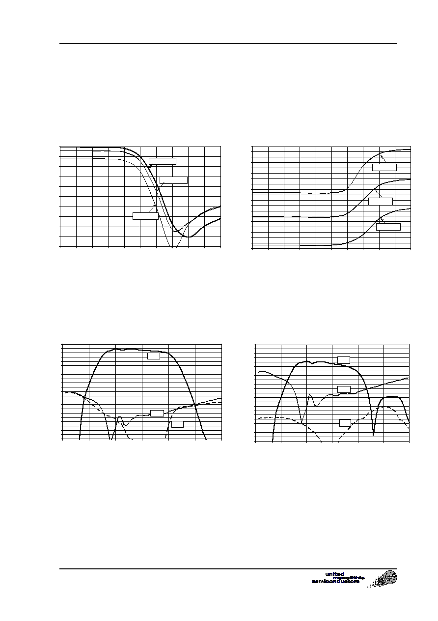
Typical On wafer measurements:
Tamb = +25∞C
Gain and phase versus voltage control on CL pad :
Sij parameter measurements versus frequency for 2 voltage control on CL pad:
CHA2097 Vd=3,5v Vg=0v Id=140mA
0
2
4
6
8
10
12
14
16
18
20
-1
-0,9
-0,8
-0,7
-0,6
-0,5
-0,4
-0,3
-0,2
-0,1
0
Vctrl (V)
S
21 (dB)
Gain at 20GHz
Gain at 30GHz
Gain at 40GHz
CHA2097 Vd=3,5v Vg=0v Id=140mA
-70
-50
-30
-10
10
30
50
70
90
110
130
150
170
190
210
230
250
270
290
310
-1
-0,9
-0,8
-0,7
-0,6
-0,5
-0,4
-0,3
-0,2
-0,1
0
Vctrl (V)
Ph
i
S2
1
(∞)
Phi at 40GHz
Phi at 30GHz
Phi at 20GHz
CHA2097 Vd=3,5v Vg=0v Vctrl=-0,3V Id=140mA
-32
-30
-28
-26
-24
-22
-20
-18
-16
-14
-12
-10
-8
-6
-4
-2
0
2
4
6
8
10
12
0
10
20
30
40
50
60
Frequency (GHz)
Ga
in
& Rlo
s
s
(d
B)
S22
S11
Gain
CHA2097 Vd=3,5v Vg=0v Vctrl=-1V Id=140mA
-22
-20
-18
-16
-14
-12
-10
-8
-6
-4
-2
0
2
4
6
8
10
12
14
16
18
20
22
0
10
20
30
40
50
60
Frequency (GHz)
Gai
n
& Rl
oss (
d
B)
S22
S11
Gain
CHA2097a
20-40GHz Variable Gain Amplifier
Ref. : DSCHA20978021
6/
8
Specifications subject to change without notice
Route DÈpartementale 128 , B.P.46 - 91401 ORSAY Cedex - FRANCE
Tel.: +33 (0)1 69 33 03 08 - Fax : +33 (0)1 69 33 03 09
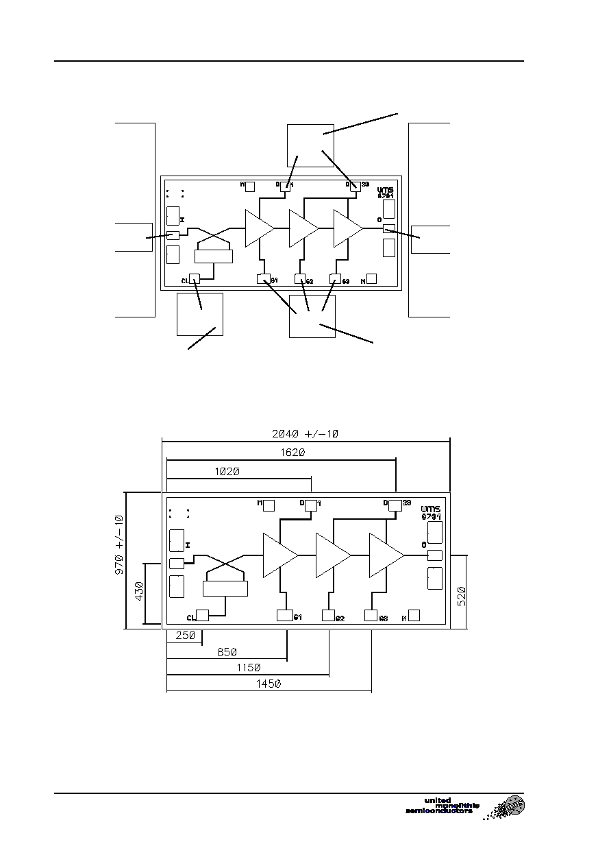
Chip Assembly and Mechanical Data
IN
OUT
To Vgs1 DC Gate supply feed
100pF
100pF
To Vd1,2,3 DC Drain supply feed
100pF
To Vgs2,3 DC Gate supply feed
To Vctrl DC supply feed
Note : Supply feed should be capacitively bypassed.
Bonding pad positions.
( Chip thickness : 100µm. All dimensions are in micrometers )
20-40GHz Variable Gain Amplifier
CHA2097a
Ref. : DSCHA20978021
7/8
Specifications subject to change without notice
Route DÈpartementale 128 , B.P.46 - 91401 ORSAY Cedex - FRANCE
Tel.: +33 (0)1 69 33 03 08 - Fax : +33 (0)1 69 33 03 09
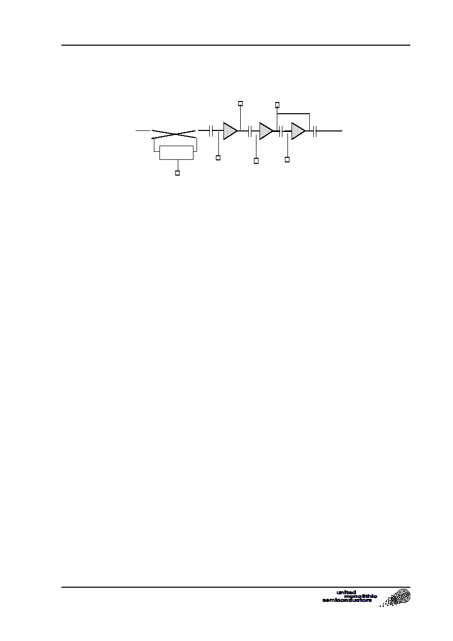
Typical Bias Tuning
The circuit schematic is given below :
Attenuator
IN
OUT
Vd 2,3
Vg 3
Vg1
Vd1
Vg 2
Vctrl
For gain control operation, The three drain biases are connected altogether. In a same way, all the
gate biases are connected together at the same power supply, tuned to drive a small signal operating
current of 140mA. A separate access to the gate voltages of each stages ( Vg1,2,3 ) is provided for
fine tuning of the stages regarding the application.
An additional pad is provided ( Vctrl ) to control the gain of the circuit, driving two cold transistors in
attenuator arrangement.
CHA2097a
20-40GHz Variable Gain Amplifier
Ref. : DSCHA20978021
8/
8
Specifications subject to change without notice
Route DÈpartementale 128 , B.P.46 - 91401 ORSAY Cedex - FRANCE
Tel.: +33 (0)1 69 33 03 08 - Fax : +33 (0)1 69 33 03 09
Ordering Information
Chip form
:
CHA2097a99F/00
Information furnished is believed to be accurate and reliable. However United Monolithic Semiconductors
S.A.S. assumes no responsability for the consequences of use of such information nor for any infringement of
patents or other rights of third parties which may result from its use. No license is granted by implication or
otherwise under any patent or patent rights of United Monolithic Semiconductors S.A.S.. Specifications
mentioned in this publication are subject to change without notice. This publication supersedes and replaces all
information previously supplied. United Monolithic Semiconductors S.A.S. products are not authorised for use
as critical components in life support devices or systems without express written approval from United
Monolithic Semiconductors S.A.S.